Note: Descriptions are shown in the official language in which they were submitted.
CA 02487711 2004-11-18
,Doc No: 102-9 CA
Patent
REDUCED SIZE TRANSMISSION LINE USING CAPACITIVE LOADING
CROSS-REFERENCE TO RELATED APPLICATIONS
[1] N/A
FIELD OF THE INVENTION
[2] The present invention relates generally to transmission line structures
in
microwave circuits and more particularly to multilayer transmission line
structures
that are capacitively loaded for the purpose of circuit size reduction.
BACKGROUND OF THE INVENTION
[3] Transmission line structures in microwave circuits are often a large
part of the
overall circuit size. Since the cost of a microwave circuit generally
increases as its
size increases, minimizing the size of transmission line structures can be of
significant importance for many applications of microwave circuits.
[4] Physical size of a transmission line is usually governed by its desired
electrical
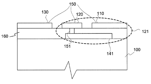
characteristics, and in many cases ¨ by a target electrical length of the
transmission
line. The electrical length of a transmission line is proportional to a ration
of its
physical length to a wavelength of the guided electromagnetic mode propagating
along the transmission line. For many applications, such as impedance matching
or in
a coupler, transmission lines of specific electrical lengths are required,
limiting thus a
minimum achievable circuit size for a type of transmission line used in a
particular
application. This size limitation can be overcome using a transmission line
structure
that is physically shorter and loading it with reactive loading to achieve an
electrical
length equivalent to a longer, unloaded transmission line.
[5] Different lengths of transmission lines have different total
inductances and total
capacitances, and therefore perform differently even at the same frequency.
The size-
reduced transmission line structures can be made electrically equivalent to
standard
transmission lines by compensating for the lower total inductance and
capacitance of
1
CA 02487711 2012-09-18
Doc. No: 102-9 CA Patent
a shortened transmission line relative to a longer transmission line. Hettak
et al, in an
article entitled "The use of uniplanar technology to reduced microwave circuit
size",
Microwave Journal, May 2001, has shown that, whereas capacitively loading the
ends of
a shortened transmission line compensates for its lower total capacitance, the
shortened
transmission line has to have a higher characteristic impedance to compensate
for its
lower total inductance. This compensation results in a size-reduced structure
having, at a
pre-determined operating frequency, the same effective characteristic
impedance and
effective electrical length as a longer transmission line.
[6] These size-reduced transmission line structures result in smaller
circuits
maintaining a target electrical performance within a given frequency range.
[7] US patent 4,127,832 issued to Riblet discloses a directional coupler
preferably
constructed in stripline or microstrip media comprising four sections of
transmission line
interconnected so as to form at their junctions four ports of the coupler,
having four
capacitive elements such as stripline or microstrip stubs connected at each
junction so
that physical length of the four sections of transmission line is reduced. In
a similar
approach, Sakagami et al, in an article entitled "Reduced branch-line coupler
using eight
two-step stubs", TEE Proc.-Microw. Antennas Propag., Vol. 146, No. 6, December
1999,
disclosed a shortened microstrip transmission line with capacitive loading
using shunt
microstrip stubs.
[8] Hirota et al, in an article entitled "Reduced-size branch-line and rat-
race hybrids
for uniplanar MMIC's", IEEE Transactions On Microwave Theory And Techniques,
Vol. 38, No. 3, March 1990, disclosed a shortened coplanar waveguide (CPW)
transmission line with capacitive loading using shunt Metal-Insulator-Metal
(MIM)
capacitors.
[9] Hettak et al, 2001, disclosed a shortened uniplanar transmission line
with
capacitive loading using shunt uniplanar stubs.
2
CA 02487711 2004-11-18
Doc No: 102-9 CA
Patent
[10] The aforementioned approaches to transmission line size reduction have
their
advantages and disadvantages.
[11] MIM capacitors at high frequencies, for example, in microwave and
millimeter-
wave wavelength regions, can be difficult to model and may be susceptible to
fabrication process deviations. In these instances, the electrical performance
of a size-
reduced transmission line may be negatively affected.
[12] Standard microstrip stubs suffer from at least two negative aspects that
limit a
total amount of size reduction. Firstly, for a given amount of capacitive
loading, a
physical length of the stub providing the loading may offset the size
reduction of the
loaded line. Secondly, standard microstrip stubs must be placed far enough
apart to
prevent electromagnetic coupling between them, usually at least a substrate
thickness
apart. This minimum spacing also limits the total amount of size-reduction.
[13] Using uniplanar stubs partially overcomes the limitations of standard
microstrip
stubs. Uniplanar stubs couple less to each other due to a uniplanar ground
conductor
= that separates them. Uniplanar stubs can also have lower characteristic
impedance
compared to standard microstrip stubs. Hence, uniplanar transmission lines and
stubs
allows more significant size-reduction compared to standard microstrip media
wherein signal and ground conductors are disposed on opposite sides of a
relatively
thick substrate. Nonetheless, size-reduction using uniplanar stubs is still
limited by
their minimum realizable characteristic impedance and a minimum spacing
between
them required for electromagnetic isolation.
[14] Recently, microwave circuits combining uniplanar transmission lines and
thin-
film microstrip (TFMS) stubs were disclosed wherein the microstrip stubs have
signal
conductors disposed in a different layer than the uniplanar transmission
lines. T. Le
Nadan et al, in an article entitled "Optimization and miniaturization of
filter/antenna
multi-function module using a composite ceramic/foam substrate", 1999 IEEE
3
CA 02487711 2004-11-18
,Doc No: 102-9 CA Patent
International Microwave Symposium, disclosed using half-wavelength TFMS stub
resonators connected to a uniplanar transmission line to form a band-pass
filter
connect to a patch antenna. TFMS stubs were used in Le Nadan solely to
increase the
isolation between the filter and the antenna.
SUMMARY OF THE INVENTION
[15] It is therefore an object of this invention to provide multi-layer
transmission
line structures electrically equivalent to physically larger uniplanar
transmission lines
using short uniplanar transmission lines capacitively loaded by TFMS shunt
stubs.
[16] It is another object of this invention to provide a method of increasing
electrical
length of a uniplanar transmission line by capacitively loading thereof using
TFMS
stubs for use in size-reduced physically compact microwave circuits.
[17] In accordance with the invention, a passive network for operating at a
microwave operating frequencyf is provided comprising a capacitively loaded
transmission line, the capacitively loaded transmission line including: a
first uniplanar
transmission line having a characteristic impedance Z1, a first end, a second
end and
an electrical length 01 therebetween; a first microstrip conductor vertically
offset from
the first uniplanar transmission line, said first microstrip conductor
electrically
connected to the first uniplanar transmission line at one location at or near
the first
end and electromagnetically coupled to a first portion of the uniplanar
transmission
line at another location, wherein the first portion of the first uniplanar
transmission
line and the first microstrip conductor form a first microstrip shunt stub for
capacitively loading the first uniplanar transmission line; there is further
provided one
of a short circuit electrically connected to the second end for short-
circuiting the
second end, and a second microstrip conductor vertically offset from the first
uniplanar transmission line, said second microstrip conductor electrically
connected
to the first uniplanar transmission line at one location at or near the second
end and
electromagnetically coupled to a second portion of the uniplanar transmission
line at
another location, wherein the second portion of the first uniplanar
transmission line
4
-
CA 02487711 2004-11-18
Doc No: 102-9 CA
Patent
= =
and the second microstrip conductor form a second microstrip shunt stub for
capacitively loading the first uniplanar transmission line; and wherein, at
the
operating frequencyf, the capacitively loaded transmission line has a pre-
determined
characteristic impedance Zo that is less than Zi and an electrical length 0 o
that is
larger than 01.
[18] In accordance with one aspect of the invention, the microstrip shunt
stubs at the
operating frequencyf are thin-film microstrip shunt stubs having a
characteristic
impedance Zs that is less than 20 C2 and an electrical length Os substantially
equal to
arctan(Zs cos(0,) ¨ cos(90))
at the operating frequencyf, and the characteristic
Zi sin(01)
impedance of the first uniplanar transmission line Zi satisfies a relation
Z Z sin(00)
, , = =
= sin(91) =
[19] In accordance with another aspect of this invention, a method is provided
for
increasing the electrical length of a uniplanar transmission line operating at
an
operating frequencyf to an increased electrical length 00, said uniplanar
transmission
line having a first end and a second end, the method comprising the steps of:
a) providing the uniplanar transmission line having a characteristic impedance
Zi
at the operating frequencyf and an electrical length Ol< 00 at the operating
frequencyfi
b) providing a first thin-film microstrip shunt stub electrically connected to
the
uniplanar transmission line at one location at or near the first end for
capacitively loading the uniplanar transmission line, said first thin-film
microstrip shunt stub comprising a microstrip conductor coupled to a first
portion of the uniplanar transmission line at another location;
c) providing a second thin-film microstrip shunt stub electrically connected
to
the uniplanar transmission line at one location at or near the second end for
capacitively loading the uniplanar transmission line, said second thin-film
CA 02487711 2004-11-18
Doc No: 102-9 CA
Patent
microstrip shunt stub comprising a microstrip conductor coupled to a second
portion of the uniplanar transmission line at another location;
wherein the characteristic impedance Z1, characteristic impedances and
electrical
lengths of the first and second microstrip shunt stubs are such that the
uniplanar
transmission line and the microstrip shunt stubs at the operating frequencyf
form a
transmission line having the increased electrical length 00> 01 between the
two
ends and a pre-determined characteristic impedance Zo < Z1;
and wherein the step (c) is only performed when the second end is not shorted.
[20] In accordance with another aspect of this invention, a passive network
for
operating at a microwave operating frequencyfis provided, the passive network
having first, second, third and fourth ports, the passive network comprising:
a) a first uniplanar transmission line electrically connecting the first and
second
ports;
b) a second uniplanar transmission line electrically connecting the third and
fourth ports;
c) a third uniplanar transmission line electrically connecting the first and
third
ports;
d) a fourth uniplanar transmission line electrically connecting the second and
fourth ports;
e) a first thin film microstrip shunt stub electrically connected to one of
the first
uniplanar transmission line and the third uniplanar transmission line at or
near
the first port for capacitively loading the first and third uniplanar
transmission
lines;
0 a second thin film microstrip shunt stub electrically connected to
one of the
first uniplanar transmission line and the forth uniplanar transmission line at
or
near the second port for capacitively loading the first and fourth uniplanar
transmission lines;
g) a third thin film microstrip shunt stub electrically connected to one of
the
second uniplanar transmission line and the third uniplanar transmission line
at
6
CA 02487711 2004-11-18
Doc No: 102-9 CA
Patent
or near the third port for capacitively loading the second and third uniplanar
transmission lines;
h) a fourth thin film microstrip shunt stub electrically connected to one of
the
second uniplanar transmission line and the fourth uniplanar transmission line
at or 'near the fourth port for capacitively loading the second and fourth
uniplanar transmission lines;
wherein the first, second, third and fourth uniplanar transmission lines, and
the first,
second, third, and fourth microstrip stubs have a common ground conductor;
wherein the first and second uniplanar transmission lines have a first
characteristic
impedance and a first electrical length smaller than 90 , and the third and
fourth
uniplanar transmission lines have a second characteristic impedance and a
second
electrical length smaller than 900;
wherein the third port is electrically connected to a substantially 50 Q load;
and
wherein the first characteristic impedance, first electrical length, second
characteristic
impedance, second electrical length and the capacitive loading by the first,
second,
third and fourth thin film microstrip stubs are such that the passive network
is capable
of operating as a branchline coupler.
BRIEF DESCRIPTION OF THE DRAWINGS
[21] Exemplary embodiments of the invention will now be described in
conjunction
with the drawings in which:
[22] FIG. lA is a diagram of a cross-sectional view of a uniplanar
transmission line
capacitively loaded by TFMS stubs.
[23] FIG. 1B is a diagram of a top view of the capacitively loaded
transmission line
shown in FIG. 1A.
[24] FIG. 2 is a diagram of a cross-sectional view of a capacitively loaded
transmission line.
7
CA 02487711 2004-11-18
Doe No: 102-9 CA
Patent
[25] FIG. 3A is a diagram of a cross-sectional view of a capacitively loaded
transmission line with signal conductors of the uniplanar transmission line
and the
TFMS shunt stubs disposed in the same layer.
[26] FIG. 3B is a diagram of a top view of the capacitively loaded
transmission line
shown in FIG. 3A.
[27] FIG. 4 is a diagram of a CPW transmission line short-circuited at one end
and
capacitively loaded at the other end with a TFMS stub using the CPW ground
conductor as ground.
[28] FIG. 5 is a diagram of a CPW transmission line short-circuited at one end
and
capacitively loaded at the other end with a TFMS stub formed by the CPW signal
conductor and the microstrip conductor.
[29] FIG. 6 is a diagram of a capacitively loaded CPW shunt short-circuit stub
implemented in a center conductor of a CPW transmission line
[30] FIG. 7A is a diagram of a capacitively loaded CPW short-circuited shunt
stub
implemented in a ground conductor of a CPW transmission line with a microstrip
conductor over a center conductor of the CPW stub.
[31] FIG. 7B is a diagram of a capacitively loaded CPW shunt short-circuit
stub
shown in FIG. 7A with a microstrip conductor over a ground conductor of the
CPW
shunt stub.
[32] FIG. 8 is a diagram of a capacitively loaded CPW series short-circuited
stub
implemented in the signal conductor of a ACPS transmission line.
[33] FIG. 9 is a diagram of a capacitively loaded CPW series short-circuited
stub
implemented in a ground conductor of a ACPS transmission line.
8
CA 02487711 2004-11-18
Doc No: 102-9 CA
Patent
#
[34] FIG. 10 is a photograph of a size-reduced branchline coupler.
[35] FIG. 11 is a chart of the method for increasing electrical length of a
UTL in
accordance with the present invention.
[36] FIG.12 is a photograph of a CPW stub capacitively loaded with a TFMS
shunt
stub with a connecting CPW section.
DETAILED DESCRIPTION OF THE PREFERRED EMBODIMENTS
[37] A first exemplary embodiment of a passive network of the present
invention is a
multi-layer capacitively loaded transmission line which is shown in FIGs. lA
and 1B,
which will now be discussed.
[38] With reference to FIG.1A, a first uniplanar transmission line (UTL) 105
is
embodied as a coplanar waveguide (CPW) formed by a signal conductor 120 and
two
ground conductors 130 and 110 on a thin dielectric film 160 supported by a
substrate
100. The thin dielectric film 160 can be a single layer of a dielectric
material or be
formed by multiple layers of dielectric materials. The signal conductor 120 is
disposed between the ground conductors 130 and 110 at a distance therefrom,
and is
typically narrower than the ground conductors. The top view of the first UTL
105 is
shown in FIG. 1B, also showing a first end 101 and a second end 102 thereof
for
connecting to other elements of a larger microwave circuit such as
input/output ports,
other transmission lines, antennas, transistors etc.
[39] Turning back to FIG. 1A, a first microstrip conductor 141 is disposed
over the
substrate 100 so that it is vertically offset from the UTL conductors and is
separated
therefrom by the thin dielectric film 160. The first microstrip conductor 141
is
connected to the CPW signal conductor 120 at a first location 151a near the
first end
101 of the UTL 105 by a via conductor 151 through the dielectric film 160. The
first
microstrip conductor 141 is oriented to extend into a region under a first
portion 112
9
,
CA 02487711 2004-11-18
Doc No: 102-9 CA
Patent
of the ground conductor 110. The first microstrip conductor 141 and the first
portion
112 of the ground conductor 110 are electromagnetically coupled through the
thin
dielectric film 160 forming a first open-circuit (o/c) thin-film microstrip
(TFMS)
shunt stub 121. In operation, the o/c TFMS shunt stub 121 provides capacitive
loading of the first end 101 of the UTL 105.
[40] Note that in the context of this specification, two conductors of a
microwave
circuit are referred to as being electromagnetically coupled to each other, if
they form
a pair of conductors, commonly referred to as signal and ground conductors, of
a
microwave waveguide capable of supporting an electromagnetic mode at an
operating
frequency of the microwave circuit.
[41] Similarly, a second microstrip conductor 142 is disposed over the
substrate 100
near the second end 102 of the UTL 105, so that it is vertically offset from
the UTL
conductors and is separated therefrom by the thin film 160. The second
microstrip
conductor 142 is connected to the central signal conductor 120 at a location
152a near
the second end 102 of the UTL 105 by a via conductor 152a through the
dielectric
film 160. The second microstrip conductor 142 is oriented to extend into a
region
under a second portion 113 of the ground conductor 110. The second microstrip
conductor 142 and the second portion 113 of the ground conductor 110 are
electromagnetically coupled through the thin dielectric film 160 forming a
second o/c
TFMS shunt stub 122 for capacitively loading the second end of the UTL 105.
[42] Alternatively, the microstrip conductors 141 and 142 can be extended
under the
ground conductor 130 to form two TFMS shunt stubs for capacitively loading the
UTL 105. Also, two TFMS shunts stubs may be located at each end 101 or 102
extending under ground conductors 130 and 110 respectively wherein their
parallel
combination is equivalent to a single TFMS stub under ground conductors 110 or
130.
CA 02487711 2004-11-18
=Doc No: 102-9 CA
Patent
[43] The aforedescribed capacitive loading using TFMS shunt stubs, in
combination
with an appropriate change of the UTL impedance as described hereinafter, has
an
effect of increasing the electrical length of the UTL as seen from the outside
network,
and thus can be used for size reduction of microwave circuits wherein a UTL of
a
particular electrical length is required by design. It however differs from
previously
published techniques wherein the capacitive loading for size reduction was
realized
by using other types of shunt stubs, such as uniplanar and standard microstrip
stubs,
and enables more size reduction as explained hereafter in this specification.
[44] TFMS transmission lines in general, and TFMS stubs in particular, are
miniaturized versions of standard microstrip lines. Like a microstrip line, a
TFMS
line is formed by two conductors vertically separated from each other by a
separating
transmission medium such as a dielectric or semiconductor layer and commonly
referred to as a signal conductor and a ground conductor. Unlike a standard
microstrip
line, however, the separating transmission medium for a TFMS line is a very
thin,
dielectric film. Preferably this thickness is about 1 micron or less.
Previously, TFMS
lines have been used on low-resistivity silicon wafers because the metal
ground plane
of the TFMS line can isolate the transmission line from the lossy silicon. For
size-
reduction of transmission lines, however, a primary advantage of using the
TFMS
shunt stubs is a low characteristic impedance of TFMS due to their thin
dielectric
film.
[45] The TFMS shunt stubs used in this invention differ somewhat from
traditional
thin film microstrip structures, as they use a portion of the uniplanar
transmission line
as a second, typically but not exclusively ground, conductor. In the first
embodiment
shown in FIGs.1A and 1B, the microstrip conductors 141 and 142 are the signal
conductors of the corresponding TFMS shunt stubs 121 and 122, which are
coupled
to the ground conductor 110 of the UTL 105. In operation, the ground conductor
110
provides a ground potential required to support microwave propagation modes
coupled to each of the microstrip conductors 141 and 142. The ground conductor
110
of the UTL 105 is therefore also a ground conductor of the first and second
TFMS
11
CA 02487711 2004-11-18
Doc No: 102-9 CA
Patent
shunt stubs. In the configuration shown in FIGs.1A, B, the microstrip
conductors 141
and 142 share thus a ground conductor with the UTL 105.
[46] The vertically offset microstrip conductors of the TFMS shunt stubs are
preferably located under the uniplanar transmission line conductors as shown
in
FIG 1A, alternatively they could be located above the UTL conductors as long
as
there is a thin dielectric material between the microstrip conductors and the
UTL
conductors.
[47] Electrical performance of a uniform transmission line at microwave
frequencies
is commonly described by two parameters: an electrical length 00, defined as
an end-
to-end phase accrual of a microwave signal propagating through the
transmission line,
and a characteristic impedance Zo. Electrical properties of a more general two-
port
network can be described by a set of parameters known in the art as ABCD
parameters, also know as a Transmission Matrix, relating electrical current
and
voltage at one port of the network to electrical current and voltage at the
other port of
the network. In a particular case of a uniform lossless transmission line
having the
electrical length 0 and the characteristic impedance Z, the ABCD parameters
satisfy
the relations (2):
[48] A = cos0, B = jZ sinO, C = (j/Z) sin , D = cos0. (2)
[49] Electrical performance of the capacitively-loaded UTL 105 approximates
the
performance of a uniform transmission line having an electrical length 00 and
a
characteristic impedance Z0 at an operating frequencyf, if the ABCD parameters
of
the capacitively-loaded UTL 105 at the operating frequencyf satisfy relations
(2) with
0 =00 and Z = Zo . The parameters 0. and Z. are referred to hereafter in this
specification as a target electrical length and a target characteristic
impedance of the
capacitively loaded UTL at the operating frequencyf At microwave frequencies,
the
ABCD parameters are typically not measured directly, but calculated from
measured
s-parameters of the network using known-in-the-art mathematical formulas. In a
12
CA 02487711 2004-11-18
= Doc No: 102-9 CA
Patent
particular microwave circuit, Zo and 90 are often pre-determined at a design
stage by
a function of the transmission line in the circuit; for example, transmission
lines
having Zo = 50 Ohm and 00 = 900 are preferably required in a directional
coupler.
[50] The UTL 105 is physically shorter than an equivalent uniform UTL having
the
electrical length O. and the characteristic capacitance Zo, and therefore has
an
electrical length Oi that is smaller than 00. To compensate for a smaller
distributed
inductance resulting from a smaller physical length, the UTL 105 has a
characteristic
impedance Z1 which is larger than Zo and satisfies at the operating
frequencyfan
expression (3):
[51] Zi =0 sin(90) (3)
sin(01)
[52] Similarly, to compensate for a smaller distributed capacitance of the
shorter
UTL 105, electrical length Os of each of the TFMS shunt stubs 121 and 122 has
to
satisfy an expression (4) to provide a correct amount of capacitive loading:
[53] 61, = arctan(Z, cos(01) ¨ cos(00))
(4)
Zo sin(80)
[54] where Zs is a characteristic impedance of the shunt stubs. For a case
when Oo =
90 , as in a directional coupler, expressions (3) and (4) were derived By
Iiettak et al.,
2001.
[55] It follows from expression (4) that a smaller Zs leads to a smaller Os,
and
therefore to shorter shunt stubs when other parameters in (4) are fixed.
Therefore,
shunt stubs that have a smaller characteristic impedance when used for
capacitive
loading of a transmission line, provide opportunities for a greater circuit
size
reduction.
13
CA 02487711 2004-11-18
=
Doc No: 102-9 CA
Patent
[56] Advantageously, the TFMS stubs of the present invention, for example the
TFMS shunt stubs 121 and 122 shown in FIGs.1A and 1B, have a much lower
characteristic impedances Z, compared to typical values of standard
microstrip.
Preferably, Z, is about or less than 20 Ohm, due to a small, about or less
than 1
micron, thickness of the dielectric film 160 separating their signal and
ground
conductors. Therefore, a more capacitive loading can be provided using TFMS
shunt
stubs compared to the standard microstrip or CPW shunt stubs of prior art,
thus
enabling more size-reduction of the passive network. Furthermore, the
microstrip
conductors 110 and 130 are more electromagnetically isolated from each other
than
for example standard microstrip stubs would be if separated by the same
distance, due
to the small separation of the TFMS conductors from their ground, and
providing an
additional advantage for circuit size reduction.
[57] Variations of the aforedescribed basic multilayer structure shown in
FIGs.1A
and 1B are of course possible. FIG.2 shows another exemplary embodiment of the
invention, which is similar to the aforedescribed embodiment shown in FIG. 1B,
but
having the order of layers wherein the UTL, the thin dielectric film, and the
conducting stubs are disposed on the substrate 100 reversed. In this
embodiment, a
signal conductor 220 and ground conductors 210 and 230 of a UTL 205 are
disposed
on the substrate 100 under the thin dielectric film 160, while a first
microstrip
conductor 241 and a second microstrip conductor, which is not shown, of the
TFMS
shunt stubs providing the capacitive loading to the UTL 205 are disposed in a
top
layer over the thin film 106.
[58] FIGs. 3A and 3B illustrate another embodiment of the aforedescribed
passive
network shown in FIGs. 1A, 1B and 2. In this embodiment, an UTL 305 is a
planar
waveguide formed by a signal conductor 320 and two ground conductors 310 and
330, and wherein the signal and ground conductors are disposed in different
layers on
opposite sides of the thin film 160. Electrical properties of such a microwave
waveguide can closely approximate electrical properties of a standard CPW, if
the
14
CA 02487711 2004-11-18
Doc No: 102-9 CA
Patent
vertical offset between the ground and signal conductors of the UTL shown in
FIGs.
3A and 38, which is defined by the thickness of the thin film 160, is very
small
compared to widths of the signal 320 and ground 310, 330 conductors of the
UTL,
and to the wavelength of the microwave signal. hi this embodiment, the
microstrip
signal conductors 341 and 342 can be disposed in the same layer as the signal
conductor 320 extending directly from the signal conductor 320 over one or
both of
the ground conductors 310 and 330, eliminating the need for an interconnect
The
order of layers wherein the signal conductor 320 and the ground conductors
310, 330
plus the microstrip conductors are disposed on the substrate can be reversed.
[59] In other embodiments of this passive network, the UTL can be a coplanar
stripline (CPS) formed by one signal conductor and one ground conductor having
substantially equal widths, or an asymmetric stripline (ACPS) formed by a
signal
conductor and a ground conductor of different widths.
[60] The aforedescribed embodiments provide a basic passive network of the
present
invention, formed by a two-port UTL and two TFMS shunt stubs capacitively
loading
opposing ends of the UTL; advantageously, this network emulates electrical
performance of a uniform UTL in a more compact footprint. Of course, in
particular
circuits many variations of this basic network and changes thereto are
possible as will
be understood by those skilled in the art, for example depending on a type of
connection thereof to other parts of the circuit and on surrounding circuit
elements.
[61] In FIG. 4, an embodiment is shown wherein one of the ends of a UTL 505 is
shorted by a interconnecting it signal conductor 520 and ground conductors
510, 530
with a metal interconnect 525 forming a short circuit. The signal conductors
520 and
the ground conductors 510 and 530 are separated from the signal conductor 520
by
gaps 511. The short-circuited UTL 505 forms a size-reduced uniplanar short
circuit
(s/c) stub that is capacitively loaded by a TFMS shunt stub 521a to increase
its
electrical length to a target value 00. Note that in this case a second TFMS
shunt stub
at the short-circuited end of the UTL is redundant and can be omitted since it
would
CA 02487711 2004-11-18
Doc No: 102-9 CA
Patent
be shorted out by the short circuit 525. Therefore, a single TFMS shunt stub
is used at
the opposite to short-circuited end of the UTL 505. The single TFMS shunt stub
has
the electrical length Os and the characteristic capacitance Zs which are
related to the
electrical length 01 and the characteristic capacitance Z1 of the UTL 505 and
to the
target parameters 00 and Zo of the loaded transmission line as defined by
expressions
(3) and (4). The CPW transmission line 505 could be an ACPS transmission line
if
one of the ground conductors 510 and 530 is removed.
[62] The microstrip conductor of a TFMS shunt stub may be oriented in any
direction under or over vertically offset portions of the UTL that provide the
second
TFMS conductor, and may either be connected to a ground conductor of the UTL
and
coupled to a portion of the signal conductor, or vice versa it can be
connected to a
signal conductor and coupled to a portion of the ground conductor as shown for
example in FIGs. lA and 1B. In some embodiments, a UTL includes an airbridge
interconnecting its ground conductors or different portions or segments or
lengths of
its ground conductors to equalize their potentials, and the microstrip
conductor can be
attached to the airbridge, electrically connecting therethrough to the ground
conductors of the UTL. Note that the term "airbridge" is not limited to and
should not
be understood as necessarily connecting means disposed in the air. For
example, in
the embodiment shown in FIGs. 1A, 1B and 2, an airbridge can be disposed in
the
same layer as the microstrip conductors, and can be connected to the ground
conductors 110, 130 or 210, 230 by vias conductors extended through the
dielectric
film 160; or for the embodiment shown in FIGs.3A and 3B, an airbridge can be
disposed in the same layer as the ground conductors 330 and 310.
[63] The aforedescribed embodiments employ TFMS shunt stubs electrically
connected to the UTL signal conductor and sharing ground conductors with the
UTL.
FIG. 5 illustrates a configuration wherein a microstrip conductor 541b is
electrically
connected to the ground conductors of the CPW UTL 505, is positioned over or
under
the UTL signal conductor 520 and coupled thereto for forming a TFMS shunt stub
52 lb. The short-circuited UTL 505 is thereby capacitively loaded by the TFMS
shunt
16
CA 02487711 2004-11-18
Doc No: 102-9 CA
Patent
stub 521b and forms a size-reduced uniplanar s/c stub. In this embodiment, the
TFMS
shunt stub 521b is formed by the microstrip conductor 541b, which is disposed
under
and along the signal conductor 520, coupled thereto through a thin film, and
is
electrically connected and joined at one end to an airbridge 580. The
airbridge 580
interconnects the ground conductors 510 and 530 of the short-circuited UTL 505
via
conducting vias 549 and 548 for equalizing electrical potentials of the
interconnected
portions of the ground conductors 510 and 530.
[64] Size-reduced UTLs capacitively loaded by TFMS shunt stubs in accordance
with present invention can be connected to any appropriate circuit elements,
including
but not limited to capacitors, inductors, resistors, transmission lines,
transistors, and
diodes. The size-reduced UTLs may also be connected to other types of passive
networks or transmission lines of the same or a different type, such as a
microstrip or
a microwave waveguide, as long as appropriate known transitions are used.
[65] The size-reduced UTLs can also be a part of a larger transmission line,
for
example as a size-reduced uniplanar s/c stub. Depending on how the size-
reduced
uniplanar s/c stub is connected to the circuit, either in series or as a
shunt, physical
layout of a corresponding network may be different. For example, layouts
wherein
standard CPW or ACPS shunt stubs are realized either inside or outside the
center
conductor are known in the art. The same is true for CPW or ACPS series stubs,
and
all of these realizations of CPW stubs may be size-reduced using TFMS shunt
stubs.
FIGs. 6 ¨9 schematically show several such embodiments.
[66] FIG. 6 shows an embodiment wherein a TFMS shunt stub 41 connected to an
aribridge 48 is used for size reduction of a s/c CPW shunt stub 65. The s/c
CPW shunt
stub 65 is formed in a central conductor 12 of the CPW transmission line
[67] FIG.7A schematically shows an embodiment wherein a microstrip conductor
741a, connected to an aribridge 748, forms a TFMS shunt stub with a s/c CPW
shunt
stub 750 and is used for size reduction thereof. FIG. 7B shows a similar
configuration
17
CA 02487711 2004-11-18
poc No: 102-9 CA
Patent
but having a differently realized TFMS shunt stub formed using a microstrip
conductor 741b, which is connected to the central conductor of the s/c CPW
shunt
stub 750 and is oriented perpendicularly thereto crossing one of the conductor
gaps
730 for coupling to a portion of the vertically offset ground electrode 710.
In fact, any
orientation of TFMS stub 741a is possible as long as proper TFMS and CPW mode
propagation is maintained.
[68] FIGs.8 and 9 illustrate embodiments wherein TFMS shunt stubs are used for
size reduction of CPW series stubs realized in ACPS transmission lines. In the
embodiment shown in FIG. 8, a size-reduced CPW series stub 850 is formed
within a
signal conductor 820 of the ACPS transmission line 805. This size-reduced CPW
series stub 850 is capacitively loaded by a TFMS shunt stub formed by a
vertically
offset microstrip 841, which is oriented along a centre conductor of the CPW
series
stub 850 and is connected to an airbridge 880 interconnecting two ground
conductors
thereof.
[69] In the embodiment shown in FIG. 9, a size-reduced CPW series stub 950 is
formed within a ground conductor 910 of an ACPS transmission line 905. The
size-
reduced CPW series stub 950 is capacitively loaded by a TFMS shunt stub 941
connected to a centre conductor of the CPW series stub 950. Airbridges 980
connect
two ground conductors of the CPW series stub 950 formed in the ground
conductor
910 of the ACPS transmission line 905.
[70] Note that the microstrip conductors of the TFMS shunt stubs shown in
FIGs.
5A, 5B, 6, 7A, 7B, 8 and 9 are disposed in a layer which is vertically offset
from the
corresponding transmission lines and is separated therefrom by a thin film
dielectric
or other suitable semi-insulating or insulating material which is not shown in
the
figures.
[71] In another embodiment of this invention, two or more TFMS shunt stubs can
be
combined in a single TFMS shunt stub if the two or more TFMS shunt stubs are
18
CA 02487711 2004-11-18
Doc No: 102-9 CA
Patent
connected in parallel at a substantially same location or at adjacent
electrically
shorted locations in a circuit, as it is common in the art. For example, in
embodiments
having a second UTL electrically connected to the first UTL at their ends, a
single
TFMS shunt stub can be employed to replace two shunt stubs capacitively
loading
joined ends of the two different UTLs.
[72] This aspect of the invention is illustrated in FIG. 10, which shows a
passive
network wherein four UTLs embodied as CPW form a size-reduced branchline
coupler 1000. In the exemplary embodiment shown in FIG.10, the coupler 1000
was
implemented on a GaAs substrate using TFMS shunt stub loading to reduce its
size in
accordance with the present invention. By way of example, this coupler was
designed
for operating at a microwave operating frequency aroundf = 44.5GHz. The
coupler
has a first port 1001, a second port 1002, a third port 1003 terminated with a
50 Ohm
resistive load 1035, and a forth port 1004. The ports are indicated in FIG.10
with
dashed lines labeled with respective numerals "1001" to "1004". A first, a
second, a
third and a forth UTLs , which are embodied as CPWs having a common ground
conductor 1030, interconnect the port pairs 1001and 1002, 1004 and 1003, 1003
and
1001, and 1004 and 1002 respectively. In FIG. 10, the first, second, third and
forth
UTLs can be identified by their respective signal conductors 1011 through
1014. For
example, the first UTL is formed by the signal conductor 1011 and two ground
conductors 1010 and 1030 separated from the signal conductor 1011 by two
symmetrical gaps 1018, which are formed on both sides of the signal conductor
1011.
Four microstrip conductors 1041-1044 are connected by posts, not shown, to the
opposing ends of the signal conductors 1011 and 1012 of the first and second
CPW
= UTLs; they are disposed in a layer which is vertically offset from the
layer wherein
the first, second, third and forth UTLs are formed, and are separated
therefrom by a
thin dielectric film having a thickness of 0.8 microns which is not shown.
[73] The passive network 1000 functions as a branchline coupler if each of the
four
branches of the coupler has electrical characteristics approximating
electrical
characteristics of transmission lines having an electrical length of 90 .
However, the
19
CA 02487711 2012-09-18
Doc. No: 102-9 CA Patent
four UTLs forming the coupler 1000 are considerably shorter and without the
TFMS
shunt stubs have electrical lengths less than rc/2 = 900. For the exemplary
embodiment
described herein, the first and second UTLs 1011 and 1012 have a first
characteristic
impedance Z1'70.70hm and a first electrical length 01' ¨ 30 deg., and the
third and
fourth uniplanar transmission lines 1013 and 1014 have a second characteristic
impedance Zr" ¨ 70.7 Ohm and a second electrical length 01" ¨45 deg. The TFMS
shunt stubs capacitively load the four UTLs, increasing their effective
electrical length
to an increased target electrical length 00 ¨ 90 . Similar to the
aforedescribed
embodiments, the parameters Or ' and Zr` of the first and second UTLs without
the
capacitive loading, and the parameters Or" and Zr" of the third and forth UTLs
without
the capacitive loading, are selected to satisfy expression (3) with the target
electrical
parameters of the capacitively loaded UTLs 00 = 7r/2 and Zo = 35.5 and 50 Ohms
for the
UTL pairs 1011, 1012 and 1013,1014 respectively. This capacitive loading of
the four
UTLs forming the branchline coupler allows approximately 65% reduction of the
circuit
area occupied by the coupler compared to a coupler without TFMS loading.
[74] Although the coupler 1000 is formed by four capacitively loaded UTLs each
of
which is similar to the capacitively loaded UTL 105 of the first exemplary
embodiment
shown in FIGs. lA and 1B, only four rather than 8 TFMS shunt stubs are used in
the
coupler 1000 to capacitively load the four UTLs at their 8 ends. This is
accomplished
using a single TFMS shunt stub to capacitively load two UTLs at their
connecting ends,
following a known in the art technique of combining capacitive loads connected
in
parallel at one location or at different but electrically shorted locations.
Further details
describing this embodiment are given in a paper by Hettak et al entitled "A
novel
compact mulit-layer MMIC CPW branchline coupler using thin-film microstrip
stub
loading at 44 GHz", 2004 IEEE International Microwave Symposium.
[75] The aforedesribed embodiments of the invention provide compact passive
networks, wherein a size reduction is achieved by employing short UTL, which,
when
CA 02487711 2004-11-18
Doc No: 102-9 CA Patent
combined with TFMS shunt stubs, within a frequency range of operation have
electrical characteristics of longer uniform UTLs of a target electrical
length eo.
[76] Accordingly, in another aspect of the present invention a method is
provided for
increasing an electrical length of a uniplanar transmission line at an
operating
frequency f to a pre-determined increased electrical length 00 from a smaller
electrical
length 01.
[77] FIG. 11 shows general steps of an exemplary embodiment of the method. In
a
first step 91, target values of the pre-determined increased electrical length
Oo and a
target characteristic impedance Zo of a transmission line at the operating
frequency f
are identified.
[78] In a next step 93, a uniplanar transmission line is provided having at
the
operating frequency f a characteristic impedance Z1 and the electrical length
Oi< 0o.
This step includes the steps of a) determining a target value of the
characteristic
impedance Z1 using for example expression (3), and b) determining a physical
layout
of the uniplanar transmission line. Step (b) may require performing computer
simulations of microwave signal propagation through the uniplanar transmission
in a
layout of the microwave circuit to ensure that the uniplanar transmission
line, when
capacitively loaded with TFMS shunt stubs at opposing ends thereof, has, at
the
operating frequency f, electrical characteristics approximately equivalent to
electrical
characteristics of a uniform transmission line having the target increased
electrical
length 00 and the target characteristic capacitance Z0; the approximate
equivalence of
electrical characteristics can be established using known in the art
techniques, e.g. by
comparing s-parameters of the corresponding networks or, as described
heretofore in
this specification, their ABCD parameters which can be simulated or extracted
from
measured s-parameters.
[79] In a further step 95, a first o/c TFMS shunt stub is provided, said first
o/c TFMS
shunt stub comprising a first microstzip conductor vertically offset from the
UTL
21
õ
CA 02487711 2004-11-18
Doc No: 102-9 CA
Patent
conductors and separated therefrom by a thin dielectric film, as shown for
example in
FIGs. lA and la The first microstrip conductor is connected to the uniplanar
transmission line at a first location at or near a first end thereof which is
not short-
circuited, and is oriented so that it is electromagnetically coupled to a
portion of the
uniplanar transmission line at a second location forming the first o/c TFMS
shunt
stub.
[80] If a second end of the UTL is not short-circuited, a second o/c TFMS
shunt stub
is provided in a step 97, said second o/c TFMS shunt stub comprising a second
-
microstrip conductor vertically offset from the UTL conductors and connected
to the
uniplanar transmission line at a third location at or near the second end
thereof. The
second microstrip conductor is oriented so that it is electromagnetically
coupled to a
portion of the uniplanar transmission line at a forth location forming the
second o/c
TFMS shunt stub.
[81] Physical dimensions and layout of the first and second TFMS shunt stubs
are
determined from a condition that the uniplanar transmission line, when
capacitively
loaded with the TFMS shunt stubs at the opposing ends thereof, has electrical
characteristics approximating electrical characteristics of a uniform
transmission line
having the target increased electrical length and the target characteristic
impedance.
This can be accomplished by first determining a target electrical length Os of
the
TFMS shunt stubs using expression (4) from the electrical length 01, the
target
electrical parameters of the transmission line 00 and Zo, and from known
characteristic impedance Zs of the TFMS shunt stub; and if necessary by using
one of
commercially available software packages for simulating electrical performance
of
microwave circuits to optimize and fine-tune the TFMS shunt stubs layout.
[82] During fabrication, steps 93,95 and 97 are preferably implemented in
parallel in
one technological process as those skilled in the art will appreciate, wherein
the
multilayer passive network of present invention is fabricated by, for example,
first
defining physical layout of all microstrip conductors on a chip by patterning
a first
22
CA 02487711 2004-11-18
Doc No: 102-9 CA
Patent
metallization layer disposed over the chip substrate, then deposing a thin
dielectric
film thereupon, patterning the thin dielectric film to form vias, deposing a
second
metallization layer over the thin dielectric film, and patterning thereof to
form the
uniplanar transmission lines and other circuit elements.
[83] During a design stage, physical layout of the capacitively loaded UTL of
the
present invention and the associated TFMS shunt stubs can be determined in
relation
to their electrical parameters Zi, Zõ 91 and Os; those skilled in the art will
appreciate
that iterative computer simulations may be required to optimize the electrical
performance of the network and it physical layout.
[84] For example, in a configuration wherein neither the first nor the second
end of
the UTL are short-circuited, the first and second TFMS shunt stubs have
preferably
same electrical characteristics; however, their physical layout can differ due
to
parasitic effects and proximal circuit elements.
[85] Note that the target electrical length Os of the TFMS shunt stub should
be
understood as an effective electrical length of the TFMS shunt stub in its
electromagnetic environment and in relation to a capacitive loading it
provides to the
UTL. For example, it should account for electrical characteristics of
interconnecting
means used to connect the TFMS shunt stub to the UTL. These interconnecting
means can include the aforementioned posts and airbridges; they can also be a
connecting section of a uniplanar transmission line.
[86] FIG. 12 shows a layout of an exemplary embodiment wherein a microstrip
conductor 1241 is connected by a connecting CPW section 1211 to a centre
conductor
1220 of a UTL embodied as a s/c CPW stub. This particular embodiment was
implemented as a part of an active microwave circuit on a GaAs substrate. The
microstrip conductor 1241 was disposed under the metal layer 1203 and
separated
therefrom by a thin dielectric layer. The UTL is foimed by conductor gaps 1218
in
the metal layer 1203. The microstrip conductor 1241 is electromagnetically
coupled
23
CA 02487711 2004-11-18
Doc No: 102-9 CA
Patent
to an overlaying portion of the metal ground plane 1203, using it as a ground
and
forming thereby an o/c TFMS shunt stub capacitively loading the s/c CPW stub.
The
metal ground plane 1203 simultaneously provides ground for both the s/c CPW
stub
and the o/c TFMS shunt stub.
[87] In summary, several exemplary embodiments of the apparatus and method of
the present invention have been described. These embodiments provide
physically
compact multiplayer passive networks based on one or more uniplanar
transmission
lines, wherein the uniplanar transmission lines have electrical lengths which
are
increased by TFMS shunt stubs capacitively loading the ends thereof, so that
the
capacitively loaded uniplanar transmission lines have pre-determined
electrical
performance approximating performance of larger uniform transmission lines.
[88] Of course numerous other embodiments may be envisioned without departing
from the spirit and scope of the invention.
24