Language selection

Search

Patent 2488075 Summary

Third-party information liability

Some of the information on this Web page has been provided by external sources. The Government of Canada is not responsible for the accuracy, reliability or currency of the information supplied by external sources. Users wishing to rely upon this information should consult directly with the source of the information. Content provided by external sources is not subject to official languages, privacy and accessibility requirements.

Claims and Abstract availability

Any discrepancies in the text and image of the Claims and Abstract are due to differing posting times. Text of the Claims and Abstract are posted:

  • At the time the application is open to public inspection;
  • At the time of issue of the patent (grant).
(12) Patent Application: (11) CA 2488075
(54) English Title: ELECTRODE STRUCTURE AND METHODS FOR MAKING AND USING SAME
(54) French Title: STRUCTURE D'ELECTRODE ET METHODES DE FABRICATION ET D'UTILISATION
Status: Deemed Abandoned and Beyond the Period of Reinstatement - Pending Response to Notice of Disregarded Communication
Bibliographic Data
(51) International Patent Classification (IPC):
  • A61N 1/04 (2006.01)
  • A61N 1/05 (2006.01)
  • C04B 41/88 (2006.01)
(72) Inventors :
  • SPECHT, HEIKO (Germany)
  • KRUEGER, FRANK (Germany)
(73) Owners :
  • W.C. HERAEUS GMBH
(71) Applicants :
  • W.C. HERAEUS GMBH (Germany)
(74) Agent: MACRAE & CO.
(74) Associate agent:
(45) Issued:
(22) Filed Date: 2004-11-19
(41) Open to Public Inspection: 2005-06-19
Availability of licence: N/A
Dedicated to the Public: N/A
(25) Language of filing: English

Patent Cooperation Treaty (PCT): No

(30) Application Priority Data:
Application No. Country/Territory Date
103 60 624.6-54 (Germany) 2003-12-19

Abstracts

English Abstract


The invention relates to an electrode structure made of noble metal or a noble
metal alloy having
a thickness of .ltoreq.100 µm for implants, as well as to three methods for
its production. The
invention further relates to the use of such an electrode structure. The
electrode structure according
to the invention distinguishes itself in that this structure has an electrode
core made of gold,
silver, copper, or an alloy of at least two of these elements and in that the
electrode core is
completely encased by a first coating, which is formed from platinum, iridium,
or ruthenium.


Claims

Note: Claims are shown in the official language in which they were submitted.


-6-
Claims
1. Electrode structure (1) made of a noble metal or a noble metal alloy having
a thickness of
.ltoreq.100 µm for implants, characterized in that the electrode structure
(1 ) has an electrode core (2)
made of gold, silver, copper, or an alloy of at least two of these elements
and in that the electrode
core (2) is encased completely by a first coating (3; 3a, 3b), which is formed
from platinum,
iridium, or ruthenium.
2. Electrode structure (1) according to Claim 1, characterized in that the
electrode core (2) has a
thickness in a range of 5 µm to 99.8 µm.
3. Electrode structure (1) according to one of Claims 1 to 2, characterized in
that the first
coating (3; 3a, 3b) has a thickness in a range of 100 nm to 5 µm.
4. Electrode structure (1) according to one of Claims 1 to 3, characterized in
that the electrode
structure (1) has a thickness in a range of 7 µm to 30 µm.
5. Electrode structure (1) according to one of Claims 1-4, characterized in
that a second coating,
which is different from the first coating (3; 3a, 3b) and which is made of
ruthenium, ruthenium
oxide, iridium, iridium oxide, platinum, or titanium nitride, is formed on the
side of the first
coating (3; 3a, 3b) facing away from the electrode core (2).
6. Electrode structure (1) according to Claim 5, characterized in that the
second coating only
covers parts of the first coating (3; 3a, 3b).
7. Method for producing an electrode structure (1) according to one of Claims
1 to 6, characterized
in that
a) an electrically insulating surface (4a) of a substrate (4) is coated with a
metal layer (5), the
metal layer (5) is then coated with photoresist (6), and the photoresist (6)
is structured,
b) a first part of the first coating (3a) is galvanically generated on the now
exposed regions of
the metal layer (5),
c) the electrode core (2) is galvanically formed on the first part of the
first coating (3a),
d) the structured photoresist (6) is then removed from the metal layer (5),
e) the metal layer (5) is removed from the electrically insulating surface
(4a) of the substrate
(4) in the regions, which are not covered by the first part of the first
coating (3a),

-7-
f) the part of the electrode core (2) still free up to now from the first
coating (3a, 3b) is galvani-
tally coated with a second part of the first coating (3b),
g) the electrode structure (1) including the metal layer (5) is detached from
the electrically insu-
lating surface (4a) of the substrate (4), and
h) the metal layer (5) is then removed from the electrode structure (1).
8. Method for producing an electrode structure (1) according to one of Claims
1 to 6, character-
ized in that
a) an electrically insulating surface (4a) of a substrate (4) is provided with
a mask, and a metal
layer (5) is formed by cathode sputtering or vapor deposition on the regions
of the electri-
tally insulating surface (4a) not covered with the mask,
b) a first part of the first coating (3a) is generated by cathode sputtering
or vapor deposition on
the metal layer (5),
c) the electrode core (2) is then formed by cathode sputtering or vapor
deposition on the first
part of the first coating (3a),
f) the mask is then removed, and
g) at least the part of the electrode core (2) still free up to now from the
first coating (3a, 3b) is
galvanically coated with a second part of the first coating (3b),
h) the electrode structure (1) is then detached from the electrically
insulating surface (4a) of the
substrate (4), in that the metal layer (5) is removed.
9. Method for producing an electrode structure (1) according to one of Claims
1 to 6, character-
ized in that
a) an electrically insulating surface (4a) of a substrate (4) is coated with a
structured metal
layer, which forms a first part of the first coating (3a),
b) the first part of the first coating (3a) is provided with a mask, and the
electrode core (2) is
formed by cathode sputtering or vapor deposition only on the first part of the
first coating
(3a).
c) the part of the electrode core (2) still free up to now from the first
coating (3a) is then gal-
vanically coated with a second part of the first coating (3b), and
d) the electrode structure (1) is then detached from the electrically
insulating surface (4a) of the
substrate (4).
10. Method according to one of Claims 7, 8, or 9, characterized in that the
electrically insulating
surface (4a) of the substrate (4) is formed from glass or plastic.

-8-
11. Method according to Claim 7 or 8, characterized in that the metal layer
(5) is formed from
copper or gold.
12. Use of an electrode structure (1) according to one of Claims 1 to 6 for
stimulation elec-
trodes, cochlear electrodes, or retinal electrodes.

Description

Note: Descriptions are shown in the official language in which they were submitted.


CA 02488075 2004-11-19
Unser Zeichen: P10284 US
25. Oktober 2004
Electrode Structure and Methods for Making and Using Same
The invention relates to an electrode structure made of a noble metal or a
noble metal alloy
having a thickness of 900 um for implants, as welt as to three methods for its
production. The
invention further relates to the use of such an electrode structure.
Electrode arrangements made of noble metal are known, for example, from WO
02/089907 A1.
There, electrode structures are formed from platinum film and are fixed on a
carrier made of
plastic material. Such electrode arrangements are used, for example, for
cochlear implants.
tJS 6,266,568 B1 discloses an expandable cochlear electrode arrangement and a
method for its
production. There, a plurality of electrode contacts spaced from each other
are arranged on a
flexible carrier.
DE-OS 35 07 623 A1 discloses a long-term implantable sheet electrode having a
physiologically
inert matrix made of flexible plastic, which is coated with an electrical
conductor, for example
made of platinum. The coating is there formed galvanically or by vapor
deposition.
It is now an object of the invention to make available another electrode
structure for implants,
which can be produced simply and e~nomic211y. Furthermore, suitable methods
for its produc-
tion, as well as its use, should be provided.
The object is achieved for the electrode structure in that this structure has
an electrode core
made of gold, silver, copper, or an alloy of at least two of these elements,
and in that the elec-
trode core is completely encased by a first coating, which is formed from
platinum, iridium, or
ruthenium.
Such an electrode structure is economical, because it has a ductile electrode
core with good
conductivity made of a more economical material, which is merely encased by a
thin, more ex-

CA 02488075 2004-11-19
_2_
pensive coating, which is corrosion-resistant and biocompatible. Optionally,
an alloy formation
can be carried out between the electrode core and the first coating by a
heating process.
It has proven effective if the electrode core has a thickness in a range of
about 5 p.m to 99.8 p,m.
For the first coating, a thickness in a range of about 100 nm to 5 pm has
proven effective. Fortn-
ing the electrode structure with a thickness in a range of about 7 p,m to 30
~m is particularly
preferred.
Preferably, a second coating, which is different from the first coating and
which is made of ru-
thenium, ruthenium oxide, iridium, iridium oxide, platinum, or titanium
nitride, is formed on the
side of the first coating facing away from the electrode core. Here, it has
proven effective if the
second coating only covers parts of the first coating.
The object is realized in a first method, wherein
a) an electrically insulating surface of a substrate is coated with a metal
layer, the metal Payer
is then coated with photoresist, and the photoresist is structured,
b) a first part of the first coating is electroplated on the now exposed
regions of the metal layer,
c) the elecVode core is electroplated on the first part of the first coating,
d) the structured photoresist is then removed from the metal layer,
e) the metal layer is removed from the electrically insulating surtace of the
substrate in the re-
gions which are not covered by the first part of the first coating,
f) the part of the electrode core still free up to now from the first coating
is electroplated with a
second part of the first coating,
g) the electrode structure inGuding the metal layer is detached from the
electrically insulating
surface of the substrate, and
h) the metal layer is then removed from the electrode structure.
The object is realized in a second method, wherein
a) an electr7cally insulating surface of a substrate is provided with a mask
and a metal layer is
formed by cathode sputter7ng or vapor deposition on the regions of the
electrically insulating
surface not covered with the mask,
b) a first part of the first coating is generated on the metal layer by
cathode sputtering or vapor
deposition,
c) the electrode core is then formed by cathode sputtering or vapor deposition
on the first part
of the first coating,

CA 02488075 2004-11-19
-3-
f) the mask is then removed, and
g) at least the part of the electrode core still free up to now from the first
coating is electro-
plated with a second part of the first coating,
h) the electrode structure is then detached from the electrically insulating
surface of the sub-
strate, in which the metal layer is removed.
The object is realized in a third method, wherein
a) an electrically insulating surface of a substrate is coated with a
structured metal layer, which
forms a first part of the first coating,
b) the first part of the first coating is provided with a mask, and the
electrode core is formed
only on the first part of the first coating by cathode sputtering or vapor
deposition,
c) the part of the electrode core still free up to now from the first coating
is then electroplated
with a second part of the first coating, and
d) the electrode structure is then detached from the electrically insulating
surface of the sub-
strate.
Such methods are excellently suited to economical and fast production of the
electrode struc-
ture according to the invention.
In this way, the electrode core can be encased with several different
coatings. To form a second
coating on the first coating, for example with the third method, the
electrically insulating surface
of a substrate must then be coated with a structured metal layer, which forms
a first part of the
second coating, and then the first part of the first coating is formed
thereon. After forming the
electrode core and the second part of the first coating, a second part of the
second coating is
finally formed. Corresponding masks are used accordingly.
Here, it has proven effective, for the three methods according to the
invention, to form the elec-
trically insulating surface of the substrate from glass or plastic. A suitable
metal layer can be
formed preferably from copper or gold.
A use of the electrode structure according to the invention for a stimulation
electrode, cochlear
electrode, or retinal electrode is ideal.
Figures 1 a to 3g will explain the electrode structure according to the
invention, as well as its
production, by way of examples. Shown are:

CA 02488075 2004-11-19
-4-
Fig. 1 several schematic diagrams of electrode structures with electrical
supply
lines in plan view,
Fig. 1a the schematic diagrams of the electrode structures from Fig. 1 in sec-
tionai view A-A',
Figs. 2a to 2d a third method for producing the electrode structure according
to the in-
vention, and
Figs. 3a to 3h a first method for producing the electrode structure according
to the in-
vention.
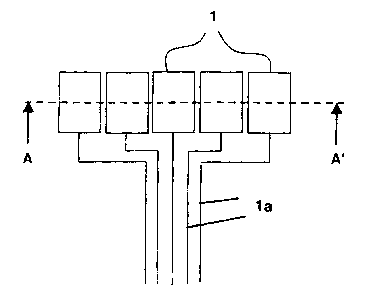
Figure 1 shows several electrode structures 1, here in an arbitrarily selected
arrangement rela-
tive to each other. Each electrode structure 1 is connected to an electrical
line 1a. However,
obviously any other arrangement can also be selected.
Figure 1a shows the section A-A' from Figure 1. Here, it can be seen that an
electrode structure
1 is constructed of an electrode core 2 and a first coating 3, which
completely surrounds the
electrode core 2.
Figures 2a-2d show the sequence of a third method according to the invention
for producing an
electrode structure 1 according to the invention. In Figure 2a, a first part
of a first coating 3a
made of iridium is vapor deposited on an electrically insulating surface 4a of
a substrate 4. Fig-
ure 2b illustrates that an electrode core 2 made of gold was vapor deposited
on the first part of
the first coating 3a. Figure 2c shows that a second part of the first coating
3b made of iridium
was galvanically deposited onto the electrode core 2. Figure 2d shows finally
the completed
electrode structure 1 detached from the substrate 4. The masks necessary for
vapor deposition
of the first part of the first coating 3a and the electrode core 2, which
cover the regions of the
substrate 4 lying next to these parts, are not shown.
Figures 3a-3h show the sequence of a first method according to the invention
for producing an
electrode structure 1 according to the invention. In Figure 3a, an
electrically insulating surface
4a made of glass for a substrate 4 is coated with a metal layer 5 made of
copper and a photore-
sist 6. The photoresist 8 is structured such that the metal layer 5 is
partially exposed via open-
ings 6a in the photoresist 6 (see Figure 3b). In the opening 6a, a first part
of a first coating 3a
made of platinum is then galvanically deposited (see Figure 3c). Figure 3d
illustrates that an
electrode core 2 made of copper was then galvanically deposited on the first
part of the first

CA 02488075 2004-11-19
-S-
coating 3a. Figure 3e shows that the photoresist 6 and also the resulting
exposed parts of the
metal layer 5 are now removed. Then, a second part of the first coating 3b
made of platinum is
galvanically generated (see Figure 3f). After removing the substrate 4, a part
of the metal layer
(see Figure 3g), which is yet to be removed, still remains on the electrode
structure. Figure 3h
shows finally the completed electrode structure 1 having the electrode core 2
and a first coating
3a, 3b.

Representative Drawing
A single figure which represents the drawing illustrating the invention.
Administrative Status

2024-08-01:As part of the Next Generation Patents (NGP) transition, the Canadian Patents Database (CPD) now contains a more detailed Event History, which replicates the Event Log of our new back-office solution.

Please note that "Inactive:" events refers to events no longer in use in our new back-office solution.

For a clearer understanding of the status of the application/patent presented on this page, the site Disclaimer , as well as the definitions for Patent , Event History , Maintenance Fee  and Payment History  should be consulted.

Event History

Description Date
Application Not Reinstated by Deadline 2010-11-19
Time Limit for Reversal Expired 2010-11-19
Inactive: Abandon-RFE+Late fee unpaid-Correspondence sent 2009-11-19
Deemed Abandoned - Failure to Respond to Maintenance Fee Notice 2009-11-19
Inactive: IPC from MCD 2006-03-12
Application Published (Open to Public Inspection) 2005-06-19
Inactive: Cover page published 2005-06-19
Letter Sent 2005-04-21
Inactive: Single transfer 2005-03-15
Inactive: Filing certificate - No RFE (English) 2005-03-07
Inactive: Courtesy letter - Evidence 2005-03-07
Inactive: IPC assigned 2005-02-18
Inactive: First IPC assigned 2005-02-18
Inactive: IPC assigned 2005-02-18
Inactive: Courtesy letter - Evidence 2005-01-18
Inactive: Filing certificate - No RFE (English) 2005-01-13
Filing Requirements Determined Compliant 2005-01-13
Application Received - Regular National 2005-01-12

Abandonment History

Abandonment Date Reason Reinstatement Date
2009-11-19

Maintenance Fee

The last payment was received on 2008-10-15

Note : If the full payment has not been received on or before the date indicated, a further fee may be required which may be one of the following

  • the reinstatement fee;
  • the late payment fee; or
  • additional fee to reverse deemed expiry.

Please refer to the CIPO Patent Fees web page to see all current fee amounts.

Fee History

Fee Type Anniversary Year Due Date Paid Date
Application fee - standard 2004-11-19
Registration of a document 2005-03-15
MF (application, 2nd anniv.) - standard 02 2006-11-20 2006-10-12
MF (application, 3rd anniv.) - standard 03 2007-11-19 2007-10-12
MF (application, 4th anniv.) - standard 04 2008-11-19 2008-10-15
Owners on Record

Note: Records showing the ownership history in alphabetical order.

Current Owners on Record
W.C. HERAEUS GMBH
Past Owners on Record
FRANK KRUEGER
HEIKO SPECHT
Past Owners that do not appear in the "Owners on Record" listing will appear in other documentation within the application.
Documents

To view selected files, please enter reCAPTCHA code :


To view images, click a link in the Document Description column. To download the documents, select one or more checkboxes in the first column and then click the "Download Selected in PDF format (Zip Archive)" or the "Download Selected as Single PDF" button.

List of published and non-published patent-specific documents on the CPD .

If you have any difficulty accessing content, you can call the Client Service Centre at 1-866-997-1936 or send them an e-mail at CIPO Client Service Centre.


Document
Description 
Date
(yyyy-mm-dd) 
Number of pages   Size of Image (KB) 
Drawings 2005-06-19 4 57
Description 2004-11-19 5 190
Abstract 2004-11-19 1 14
Claims 2004-11-19 3 96
Claims 2004-11-19 4 57
Representative drawing 2005-05-25 1 4
Cover Page 2005-06-06 1 32
Filing Certificate (English) 2005-01-13 1 158
Filing Certificate (English) 2005-03-07 1 158
Courtesy - Certificate of registration (related document(s)) 2005-04-21 1 104
Reminder of maintenance fee due 2006-07-20 1 110
Reminder - Request for Examination 2009-07-21 1 115
Courtesy - Abandonment Letter (Maintenance Fee) 2010-01-14 1 174
Courtesy - Abandonment Letter (Request for Examination) 2010-02-25 1 165
Correspondence 2005-01-13 1 27
Correspondence 2005-03-07 1 26