Note: Descriptions are shown in the official language in which they were submitted.
CA 02488091 2004-12-O1
Patent Specification
Polysiloxane Film and Method of Manufacturing Thereof
Technical Field of the Invention
The present invention relates to a self supporting polysiloxane film, and more
specifically, to an optically transparent polysiloxane film of superior heat
endurance.
Specifically, the present invention provides a polysiloxane film that can be
used as a
transparent electrode film, a TFT electrode film, or a film used for other
optoelectroriics
elements; it can also be used for wavelength filters, polarizers, and other
optical elements,
or as an electronics material of superior heat endurance and insulating
properties. The
aforementioned polysiloxane film mayor may not have an inorganic layer.
Backgrounds of the Invention
In recent years, lightweight transparent polymer filins have been extensively
used
in the field of displays, as can be seen in the example of cellular phone
displays. 1n
addition, polymer films are considered to be one of the indispensable
constituent
elements of conventional paper displays.
Currently known films, which constitute one of the most suitable technological
fields for polymer materials, include various films of polyethylene,
polypropylene,
polyethylene terephthalate, and other crystalline polymeric films as well as
films of
polycarbonate, polymethylmethacrylate, and other amorphous polymers. All of
the
above-mentioned materials are thermoplastic polymers that readily lend
themselves to
use in the production of various types of films by adjusting their molecular
weight and
molecular weight distribution.
Many of the currently commercially available transparent polymer films are
made
of thermoplastic polymers and are manufactured, for instance, by calendering
molten
thermoplastic polymers or by means of extrusion molding them using a T-die. In
addition, transparent films can be produced by biaxially stretching
crystalline polymers.
Films made from thermoplastic polymers are known to be prone to molecular
chain orientation that results from the method of their manufacturing.
In the case of transparent films, such orientation phenomena present a
particularly
serious problem. This is because birefringence that results from light passing
through a
transparent film whose molecular chains have been oriented causes polarization
of light.
Therefore, in terms of their practical application as optical materials,
thermoplastic
polymer-based transparent films have been viewed as problematic.
Although the orientation of thermoplastic polymers is caused by the stress
applied
thereto in the molten state, the application of a certain amount of stress
during molding in
the molten state is impossible to avoid. Therefore, in order to suppress the
orientation of
CA 02488091 2004-12-O1
2
the film, it is a good idea to select a molding treatment that does not
produce stress, such
as, for instance, cast molding with the use of a solvent. However, cast
molding requires
that a casting solution be prepared by dissolving a mixture of a thermoplastic
polymer
with various additives such as a UV absorption agent, antioxidant, etc.
Known in the art are thermoplastic amorphous polymers of high thermal
resistivity, such as polysulfone. However, a light-absorption band may exist
in
polysulfones approximately up to 400 nm, and from this point of view, this
polymer
cannot be easily obtained with high optical transmissivity.
On the other hand, in the case of thermosetting resins, molding does not need
application of pressure since liquid monomers or low-molecular-weight
prepolymers are
subject to cross-linking and increase in molecular weight. This prevents
orientation of
polymer molecular chains.
Normally, films made from thermosetting resins are supplied in shapes that can
be
maintained by being supported on appropriate substrates, and in many cases is
it is quite
difficult to obtain a self supporting film that is not intended for being
maintained on a
substrate.
Polysiloxanes can be produced in the form of transparent films that possess
superior thermal stability, UV ray stability, anti-oxidation stability, etc.
without addition
of heat-resistance stabilizers, UV absorbants, anti-oxidants, or the like.
However, they
are intended for being supported by substrates, and self supporting
polysiloxane films
having sufficient physical properties are still absent on the market.
Disclosure of the Invention
It is an object of the invention to provide a self supporting polysiloxane
film that
is characterized by excellent permeability to light in a visible-light
wavelength range,
low birefringence, and physical properties suitable for practical application.
It is another
object of the invention to provide a laminated film that consists of a
transparent layer
made from the aforementioned polysiloxane film and a layer of an inorganic
material
placed onto the aforementioned transparent layer.
The object of the present invention is attained by providing a polysiloxane
filin
consisting of a polysiloxane obtained by crosslinking a polysiloxane having
unsaturated
aliphatic hydrocarbon group in one molecule and represented by the average
structural
formula: (1) R18Si0~4_ay2 (where Rl is a Cl~Clo monovalent hydrocarbon group
and the
subscript «a» is a positive number in the range of 0<a<2) (hereinafter
referred to as the
"polysiloxane of the above-mentioned average stnzctural formula (1)") with an
organosilicon compound having, in each molecule, at least two hydrogen atoms
directly
bonded to silicon atoms (hereinafter referred to as the "above-mentioned
organosilicon
compound"); crosslinking being carried out in the presence of a platinum
catalyst.
CA 02488091 2004-12-O1
3
The polysiloxane film of the present invention can be produced by following
the
steps of: forming an uncured film by coating a substrate with a film-forming
crosslinkable polysiloxane composition comprising the polysiloxane of the
above-
mentioned average structural formula (1), the above-mentioned organosilicon
compound,
and a platinum catalyst; obtaining a cuxed film by crosslinking the above-
mentioned
uncured film; and peeling off the above-mentioned cured film from the above-
mentioned
substrate.
The polysiloxane of the above-mentioned average structural formula (1} may
consists of (XRzzSiOln) units (where X is a Cz~Clo monovalent unsaturated
aliphatic
hydrocarbon group and Rz is independently a Cl~Cio monovalent hydrocarbon
group
other than X) and (R3SiO3n) units (where R3 is a CI~C~o monovalent hydrocarbon
group
other than X) as essential constitutional units.
Furthermore, the polysiloxane of aforementioned structural formula (1) may
consist of (Ra"SiOt~n~z) units (where Ra is independently a group selected
from a C~~Cio
monovalent hydrocarbon group and a Cz~Clo monovalent unsaturated aliphatic
hydrocarbon group; and <m» is 1, 2, or 3) and (SiOan) units and contain
unsaturated
aliphatic hydrocarbon group in one molecule.
One example of the polysiloxane of the aforementioned average structural
formula (1) is a polysiloxane that consists of (XRzzSiOt,z) units (where X and
Rz are the
same as defined above) and (R3Si03n) units (where R3 is the same as the one
defined
above). Methods of manufacturing of such a polysiloxane are also known. For
example it
can be produced by subjecting R3SiC13 to hydrolysis and causing a reaction
between the
hydrolysis product and a compound having an XRzzS~. group, e.g., an
XRzzSiOSiRzzX
disiloxane.
Another example of the polysilaxane of aforementioned average structural
formula (1) is a polysiloxane that consists of (Ra~SiOta_"~z) units (where Ra
and "n " are
the same as defined above) and (SiOa~z) units and that contains unsaturated
aliphatic
hydrocarbon groups in one molecule. Methods of manufacturing such a
polysiloxane are
also known. For example it can be produced by introducing (Ra3SiO~n) units
(n=3) into a
product of hydrolysis and condensation of an orthosilicate and a
tetraalkoxysilane (that
contains SiOan pits) due to reaction thereof with a compound having R4Si
groups, such
as R4SiCl, RaSiOSiRa3, etc. (in this case, in the initial stage the reaction
is carried out
with a compound having Ra3Si groups without unsaturated aliphatic hydrocarbon
groups
and then, for introduction of unsaturated aliphatic hydrocarbon groups, with a
compound
having Ra3Si groups that contains the aforementioned unsaturated aliphatic
hydrocarbon
groups). Furthermore, (Ra3SiOl~z) units (n=3) and (RazSiO) units (n=2) can be
introduced
by reacting the aforementioned products of hydrolysis and condensation with a
compound that contain Ra3Si groups, such as Ra3SiCl, Ra3SiOSiRa3, etc.
Similarly,
(R4S103~} units (n=1) can be introduced by reacting the aforementioned
products of
hydrolysis and condensation with R4SiCl3 or its derivatives.
CA 02488091 2004-12-O1
4
The polysiloxane film of the present invention possesses self supporting
properties, does not have a specific light absorption band in the visible
wavelength range and has an
optical transmissivity of not less than 85% at 400 nm and an optical
transmissivity of not
less than 88% in the wavelength range of from 500 nm to 700 nm.
Thus, the object of the present invention is accomplished by providing a
laminated film formed by depositing an inorganic layer onto a transparent
layer made
from the aforementioned polysiloxane film. Preferably, the inorganic layer is
formed
from a vapor-deposited metal or a semiconductor metal oxide. For example, the
aforementioned inorganic layer may be formed by vapor deposition in vacuum at
a
temperature nat exceeding 300°C, preferably not exceeding 250°C.
Brief Description of the Drawings
Fig. 1 shows absorption spectra of transparent laminated films of four
different types
obtained in Practical Example 6 for different durations of inorganic-layer
formation steps.
Detailed Description of the Invention
The crosslinkable polysiloxane composition used in the production of the
polysiloxane film of the present invention is comprised of the polysiloxane of
the above-
mentioned average stntctural formula (1), the above-mentioned organosilicon
compound,
and a platinum catalyst as indispensable components.
The polysiloxane of the above-mentioned average structural formula (1) used in
the present invention comprises C1~C18, preferably, C1~C6, and even more
preferably, Cl
or C2 monovalent saturated hydrocarbon groups and/or C2~Cio, preferably,
Cz~CB, and
even more preferably, CZ~C6 and especially C2~C4 monovalent unsaturated
hydrocarbon
groups (both types of groups are designated as Rl in the above-mentioned
average
structural formula (1)). The Cz~Clo unsaturated hydrocarbon groups are made up
of
C2~Clo unsaturated aliphatic hydrocarbon groups and C6~Clo aromatic
hydrocarbon
groups, but the polysiloxane of the above-mentioned average structural formula
(1) of
the present invention should necessarily contain in one molecule at least two
such
unsaturated aliphatic hydrocarbon groups.
Methyl, ethyl, n-propyl, isopropyl, n-butyl, isobutyl, sec-butyl, tert-butyl,
pentyl,
hexyl, heptyl, octyl, nonyl, decyl and other alkyl groups are suggested as the
Cl~Cio
saturated hydrocarbon groups. Methyl is preferable from the standpoint of the
heat
endurance and other properties of the polysiloxane.
Vinyl, 1-propenyl, allyl, isopropenyl, 1-butenyl, 2-butenyl, and other alkenyl
groups are suggested as the Cz~Clo unsaturated aliphatic hydrocarbon groups.
Vinyl is
preferable from the standpoint of the crosslinking reactivity and other
properties of the
polysiloxane.
CA 02488091 2004-12-O1
Phenyl, tolyl, xylyl, etc. are suggested as examples of the C6~Clo aromatic
hydrocarbon groups. Phenyl is preferable from the standpoint of the heat
endurance and
other properties of the polysiloxane.
The polysiloxanes of the above-mentioned average structural formula (1) used
in
the present invention include polysiloxanes comprising trifunctional units and
monofunctional units as well as polysiloxanes consisting of tetrafunctional
units and
monofunctional units. In addition, as far as the polysiloxanes of the above-
mentioned
average structural formula (1) are concerned, the use of bifunctional units is
not
particularly excluded and, depending on the purpose and intended use,
bifunctional units
may also be used. However, generally speaking; although the introduction of
bifunctional units into polysiloxane leads to increased flexibility of the
resultant film, it
also brings about a decrease in the thermal deformation temperature of the
film and
thereby creates an important factor that affects its shape, which is why the
content of
bifunctional units is limited to a range in which the effects of the present
invention are
not impaired.
Qualitatively, it can be appreciated that the flexibility of the polysiloxane
filin of
the present invention increases as the distance between crosslinking points
becomes
longer and its brittleness increases as the distance between crosslinking
points becomes
shorter. In order to reduce the distance between crosslinking points it is
preferable to
select low molecular weight compounds as the polysiloxanes of the above-
mentioned
avezage structural formula (1) and compounds having as many silicon-bonded
hydrogen
atoms as possible as the above-mentioned organosilicon compounds. On the other
hand,
in order to increase the distance between crosslinking points, it is
preferable to choose
high molecular weight compounds as the polysiloxanes of the above-mentioned
average
structural formula (1) and compounds having as few silicon-bonded hydrogen
atoms as
possible as the above-mentioned organosilicon compounds. In this manner, the
mechanical properties of the polysiloxane film of the present invention can be
controlled
by appropriately selecting the number of hydrogen atoms in the above-mentioned
organosilicon compound and the molecular weight of the polysiloxane of the
above-
mentioned average structural formula (1).
The polysiloxane of the above-mentioned average structural formula (1) may
consists of (XR22SiOln) units (where X and RZ are the same as defined above)
and
(R3Si03n) units (where R3 is the same as defined above), or (R4~,SiOta-~"~)
units (where R4
and <m» are the same as defined above) and (Si~4~) units as essential
constitutional units.
This polysiloxane also contains in its molecule unsaturated aliphatic
hydrocarbon groups.
Molecular weights and mole ratios of the aforementioned structural units may
vary in
wide ranges and may be freely selected provided that the optical
transmissivity is not less
than 85% at 400 nm, and is not less than 88% in the wavelength range of from
S00 nm to
700 nm, and that the tensile strength of the film is not less than 10 MPa.
There are no particular limitations concerning the above-mentioned
organosilicon
compounds used in the present invention so long as these are compounds
containing, in
each molecule, two or more hydrogen atoms directly bonded to silicon atoms; it
is
CA 02488091 2004-12-O1
6
preferable to use compounds possessing compatibility with the polysiloxanes of
the
above-mentioned average structural formula (1) in the presence of organic
solvents or in
the absence thereof. The above-mentioned organosilicon compounds can be either
synthesized using typical means employed in the pertinent technical field or
obtained
commercially.
Specific examples of the above-mentioned organosilicon compounds are provided
below:
(1) Methylsilane, dimethylsilane, phenylsilane, diphenylsilane,
phenylmethylsilane,
phenyltris(dimethylsiloxy)silane, and other silane-based organosilicon
compounds;
(2) 1,2-bis(dimethylsilyl)benzene, 1,3-bis(dimethylsilyl)benzene, 1,4-
bis(dimethylsilyl)benzene, and other aromatic organosilicon compounds;
(3) Me3Si0-(Me2Si0)m (MeHSiO)"-SiMe3 (where <an» is an integer of 0 or 1 and
<m»
is an integer of 2 or greater) and other methylhydrogenpolysiloxanes having
both
ends of the molecular chain blocked by trimethyl groups;
(4) HMe2Si0-(MeZSiO)p-(MeHSiO)q-SiMezH (where the subscripts «p» and «q» are
independently 0 or integers of f or greater), for instance, 1,1,3,3,5,5,7,7-
octamethyltetrasiloxane, and other methylhydrogenpolysiloxanes capped with
hydrogen atoms at both ends of the molecular chain;
(5) Me3Si0-(PhMeSiO)m (MeHSiO)"-SiMe3, Me3Si0-(PhMeSiO)m (PhHSiO)n
SiMe3 (where the subscript <an» is 0 or an integer of 1 or greater and the
subscript
<m» is an integer of 2 or greater) and other methylphenylhydrogenpolysiloxanes
having both ends of the molecular chain blocked by trimethyl groups;
(6) HMe2Si0-{PhMeSiO~-(MeSiHO)q-SiMe2H, HMe2Si0-(PhMeSiO)p {PhSiHO)q-
SiMe2H, HMe2Si0-[(Me2HSi0)PhSiO]pSiMeZH {where the subscripts «p» and
«q» are independently 0 or integers of 1 or greater) and other
methylphenylhydrogenpolysiloxanes capped with hydrogen atoms at both ends of
the molecular chain;
(7) (Me2Si0)m(MeHSiO)n, (PhMeSiO)m(PhHSiO)", (PhMeSiO)m(MeHSiO)n (where
<Qn» is 0 or an integer of 1 or greater and <m» is an integer of 2 or
greater), for
instance, phenylhydrocyclosiloxane (3- or 4-mers) and other cyclic
polysiloxanes;
(8) Bis[(p-dimethylsilyl)phenyl]ether and other ether-type organosilicon
compounds;
(9) PhSi(OSiMeZH)l.sOo.~s~ PhSi(OSiMe2H)ZOo,s, PhSi(OSiMeZH)Z,sOo.is~
PhSi(OSiMe2H)1,~(OMe)o.o60o.s2, {(HMe2SiO) 3SiC6Fi4)2,
(HMeZSiO)3SiC~Si(OSiMe2H)3 and other organosilicon compounds;
(10) Silicone resin compounds comprising RsbR6~SiOt4_~~n units (where Rs is Me
or
Ph, R6 is H, the subscript «b» is an integer in the range of 0 to 2, the
subscript «c»
is an integer in the range of 1 to 3, and «b+c» is an integer of 3 or less)
(where the
compounds comprise at least two atoms of hydrogen per molecule), etc. (in all
the
formulas above, Me represents methyl and Ph represents phenyl).
Theoretically; if the mole ratio of the silicon-bonded hydrogen atoms of the
above-
mentioned organosilicon compound to the unsaturated aliphatic hydrocarbon
groups in
the polysiloxane of the above-mentioned average structural formula (1) is 1:1,
both the
polysiloxane of the above-mentioned average structural formula (1) and the
above-
CA 02488091 2004-12-O1
7
mentioned organosilicon compound are supposed to react completely, but in
reality a
certain amount does not react and remains in the material as residue.
The amount of unsaturated aliphatic hydrocarbon groups remained after cross-
linking can be as much as possible reduced by increasing the amount of silicon-
bonded
hydrogen atoms as compared to the unsaturated aliphatic hydrocarbon groups.
Thus, it
becomes possible to reduce deterioration that may be caused by ultraviolet
rays oxygen
and, hence, to improve optical transmissivity. However, using an excessive
amount of the
organosilicon compound relative to the polysiloxane of the above-mentioned
average
structural formula (1) causes problems in terms of reaction efficiency and in
other
respects. In the film-forming crosslinkable polysiloxane composition of the
present
invention, the above-mentioned organosilicon compound is usually combined with
the
polysiloxane of the above-mentioned average structural formula (1) such that
the number
of hydrogen atoms directly bonded to silicon atoms contained in the above-
mentioned
organosilicon compound is equivalent to or greater than the number of the
aliphatic
unsaturated groups contained in the polysiloxane of the above-mentioned
average
structural formula (1). However, because unreacted residual silicon-bonded
hydrogen
atoms may react with moisture to produce silanol groups, the amount of the
above-
mentioned organosilicon compound has to be kept within certain limits to
prevent the
generation of silanol groups, with account taken of the intended use of the
film-forming
crosslinkable polysiloxane composition. The amount of the above-mentioned
organosilicon compound can be varied between 10 and 120 parts by mass per 100
parts
by mass of the polysiloxane of the above-mentioned the average structural
formula (1),
on the condition that the molar ratio of the hydrogen atoms of the above-
mentioned
organosilicon compound to the aliphatic unsaturated groups of the polysiloxane
of the
above-mentioned average structural formula (1) is 1:1 or greater, preferably
1.11.5.
For optical material applications, it is particularly desirable for the
polysiloxane
film of the present invention to be transparent in the visible wavelength
range. In oxder
to increase the transparency of the polysiloxane film of the present
invention, it is
necessary to provide that the hydrocarbon groups bonded to the aforementioned
organosilicon compound and the hydrocarbon groups other than those of the
unsaturated
aliphatic hydrocarbon groups of the polysiloxane of average structural formula
(1} be as
much as possible the same. For example, when the polysiloxane of the above-
mentioned
average structural formula (1) contains mainly phenyl groups as the Rl groups,
it is
recommended that the above-mentioned organosilicon compound should similarly
have
phenyl groups directly bonded to silicon atoms.
Any platinum catalyst normally used for the hydrosilation reaction and in the
crosslinking of silicone rubber can be utilized as the platinum catalyst added
to the film-
forming crosslinkable polysiloxane composition of the present invention.
Examples of
such platinum catalysts include platinum chloride; chloroplatinic acid,
platinum-olefin
complexes, platinum-phosphine complexes, platinum-vinylsiloxane complexes,
etc.
Addition-reaction catalysts represented by known palladium-compound catalysts
and
rhodium-compound catalysts also may be used for the same purpose. There are no
particular limitations concerning the amount of the platinum catalyst added,
which is, for
CA 02488091 2004-12-O1
instance, approximately 0.0000013 wt%, as converted to platinum metal,
relative to the
total weight of the crosslinkable polysiloxane composition, or approximately
0.5100
ppm, as converted to platinum metal, relative to the total amount of the
polysiloxane of
the above-mentioned average structural formula (1) and the above-mentioned
organosilicon compound, and depending on the specific ingredients of said
composition,
the amount of the added catalyst can be appropriately increased or reduced.
In addition to the above-mentioned essential ingredients, the crosslinkable
polysiloxane composition of the present invention may contain optional
additives
intended to impart the film with the desired physical properties, for
instance, various
fillers, fibers, etc. that are commonly compounded with polysiloxanes.
For instance, when a high optical transparency is not required of the film,
the
strength of the film can be improved by adding common particulate additives,
such as
silica (including fumed silica and colloidal silica), alumina, and other
inorganic particles
as additives. The amount of the inorganic particles, which may also vary
depending on
the target physical properties and specific application, may be determined on
the basis of
simple compounding tests.
Additionally, even if inorganic particles are added, the transparency of the
film
can be preserved by adjusting the particle size of said particles. The
increase in the
opacity of the film due to the particulate additives is caused by light
scattering due to the
particulate additives and varies depending on the refractive index of the
material of the
particles; however, in general, selecting particles with a diameter of 1151/6
of the
wavelength of the incident light (that in the range of visible wavelength
light
corresponds to 80 to 60 nm), makes it possible to suppress scattering and
maintain the
transparency of the film.
Secondary aggregation of particles may also constitute a serious source of
light
scattering. The secondary aggregation may be restricted by subjecting the
particle to
surface treatment.
Phthalocyanine-based colorants, conventional fluorescent materials, and other
dyes and pigments can be also added to the present crosslinkable polysiloxane
composition used for polysiloxane filin manufacture. In particular, since the
polysiloxane
film of the present invention does not have a specific absorption in the
visible wavelength range, it is
possible to functionalize the polysiloxane film of the present invention by
using additives
that absorb visible light and carry out specific functions as a result of
photo-excitation.
Next, explanations are provided regarding the production process used for the
polysiloxane film of the present invention.
The polysiloxane film of the present invention can be obtained by means of
film
molding using a crosslinkable polysiloxane composition containing the
polysiloxane of
the above-mentioned average structural formula (1), the above-mentioned
organosilicon
compound, and a platinum catalyst. Specifically, during film molding, a series
of
CA 02488091 2004-12-O1
9
operations is carried out that involves forming an uncured film by coating the
aforementioned crosslinkable polysiloxane composition on a substrate,
crosslinking and
curing said uncured film, and peeling off the cured film from said substrate.
The above-mentioned crosslinkable polysiloxane composition for film molding
can be prepared by dissolving the polysiloxane of the above-mentioned average
structural
formula (1), the above-mentioned organosilicon compound, and the platinum
catalyst in a
solvent of the manufacturer's choice. The amount of the solvent added may be,
for
instance, in the range of from 1 part by mass to 300 parts by mass per 100
parts by mass
of the polysiloxane composition for film molding, but it is not limited to
this range. In
the process of crosslinking the temperature may sometimes reach as high as
200°C or so,
and thus there are no particular limitations with regard to the solvents used
so long as the
solvents have a boiling point of not more than 200°C and are capable of
dissolving
polysiloxanes. The solvents may be exemplified by acetone, methylethylketone,
or other
ketones; benzene, toluene, xylene, or other aromatic hydrocarbons; heptane,
hexane,
octane, and other aliphatic hydrocarbons; dichloromethane, chloroform,
methylene
chloride, 1,1,1-trichloroethane, or other halogenated hydrocarbons; THF, or
other ethers;
dimethylformamide, N-methyl pyrrolidone, or other organic solvents.
As follows from the above, in order to reduce as much as possible the amount
of
unsaturated aliphatic hydrocarbon groups that remain after cross-linking and
thus to
improve the optical transmissivity, I1V-resistant properties, acid-resistant
properties, etc.,
it is preferable to control the amount of the added organosilicon compound and
the
polysiloxane of the aforementioned average structural formula (1) in the
aforementioned
crosslinkable polysiloxane composition for film molding such that the amount
of
hydrogen atoms in the organosilicon compound is slightly in excess relative to
the
amount of the unsaturated aliphatic hydrocarbon groups in the polysiloxane of
the
aforementioned average structural formula (1).
Although there are no particular limitations regarding the substrate so long
as it has
excellent peelability and a smooth surface, the material has to be stable to
the essential
components of the crosslinkable polysiloxane composition, i.e. the
polysiloxane of the
aforementioned formula (1), the aforementioned organosilicon compound, and the
platinum catalyst, as well as to the solvents and additives used when said
composition
contains solvents or additive. In addition, it must exhibit resistance in the
temperature
environment used for the crosslinking reaction of the uncured film. Glass,
graphite, and
other inorganic substances, iron, stainless steel, and other metallic
materials, or stable
polymeric materials that are not dissolved in the solvents used for cast
molding even at
boiling points of such solvents, can be used as the substrate materials.
The crosslinking (curing) of the uncured film can be corned out by heating
said
film to room temperature or a higher temperature. There are no particular
limitations
concerning the temperature, to which it is heated, so long as it is room
temperature or
higher, for instance, a temperature of 40°C to 200°C. The
heating-induced hydrosilation-
type addition reaction between the polysiloxane of the aforementioned average
formula
(1) and the aforementioned organosilicon compound is catalyzed by the
aforementioned
CA 02488091 2004-12-O1
platinum catalyst. If necessary, the method of heating employed can be
appropriately
modified. For example, heating can be done in multiple short spurts, or
continuously
over an extended period of time.
Additionally, in order to improve workability by adjusting platinum catalyst-
dependent reactivity during crosslinking and curing, 2-methyl-3-butyn-2-ol,
dimethylmaleate, dimethylfiunarate, bis(2-methoxy-1-methylethyl)maleate, 1-
ethynyl-1-
cyclohexanol, 3,5-dimethyl-1-hexyn-3-ol, N,N,N',N'-tetramethylethylenediamine,
ethylenediamine, diphenylphosphine, diphenylphosphate, trioctylphosphine;
diethylphenylphosphonite, methyldiphenylphosphinite, and other cure retarders
can be
added in advance to the crosslinkable polysiloxane composition as reaction
controllers.
A film cured on a substrate by means of crosslinking can be obtained by
peeling
from the substrate using peeling means well-known in this technical field.
Mechanical
separation means utilizing, for instance, doctor blades, vacuum suction, etc.,
can be used
as the peeling means. The thickness of the polysiloxane film of the present
invention,
which can be appropriately changed depending on the intended use, is typically
between
5 and 200 ,can or greater.
The thus produced polysiloxane film of the present invention, unlike films
produced by the cast molding of ordinary thermosetting resins, is a self
supporting
substrate-independent film. In addition, the polysiloxane film of the present
invention
does not have a specific light absorption band in the visible wavelength range
and has an optical
transmissivity of not less than 85% at 400 nm and an optical transmissivity of
not less
than 88% in the wavelength range of from 500 nm to 700 nm.
Also, the polysiloxane film of the present invention is problem-free in terms
of
polymer chain orientation because it is produced without applying stress in a
molten state.
For this reason, birefringence is so low that it can be ignored.
The polysiloxane film of the present invention is obtained by polymerization
as a
result of an addition-type crosslinking reaction taking place between the
unsaturated
aliphatic hydrocarbon groups of the polysiloxane of the aforementioned average
structural formula (1) and hydrogen atoms directly bonded to silicon atoms in
the
aforementioned organosilicon compound. In such an addition-type crosslinking
reaction,
low molecular weight by-products are not generated during crosslinking, and
for this
reason crosslinking-induced reduction in the volume of the film is suppressed
and made
smaller in comparison with the condensation-type crosslinking reaction seen in
ordinary
thermosetting resins. For this reason, the internal stress in the resultant
film is lower in
the case of polysiloxane films obtained by the addition-type crosslinking
reaction.
Therefore, in the polysiloxane film of the present invention, the generation
of strain
caused by the internal stress is suppressed. Additionally, this positively
contributes to an
increase in the strength and an increase in the optical uniformity of the
film.
CA 02488091 2004-12-O1
11
In addition, even if heated to 300°C, the polysiloxane film of the
present
invention maintains its shape and exhibits no changes in weight. In addition,
it exhibits
superior mechanical properties after heating, there being almost no change
before and
after heating in terms of the mechanical properties of the polysiloxane film
of the present
invention. Therefore, the polysiloxane film of the present invention possesses
the high
heat endurance characteristic of polycarbonates and other widely-used
engineering
plastics and can be suitably employed in technical fields requiring heat
endurance.
As has been mentioned above, the laminated film of the invention is provided
with an inorganic layer placed onto the above-described cross-linked
polysiloxane film.
The transparent layer that constitutes a substrate of the laminated film of
the
invention may be comprised of a single layer of the cross-linked polysiloxane.
If
necessary, however, the substrate may be comprised of a laminated body
composed of a
plurality of individual cross-linked polysiloxane films, or may be composed of
a cross-
linked polysiloxane film laminated with a transparent film or sheet of another
type.
Since, in general, polymer films possess flexibility and electrical insulation
properties, they are suitable for use as substrates for films of many other
types. For
example, the polymeric film substrates may support a-Si {H} (amorphous
silicon), p-Si
(polycrystalline silicon), transparent electrode substances, or other film-
formed electrode
elements; wavelength-dividing filters for optical communication, band filters,
or filters
of other types; antireflective films made from antireflective film materials;
gas-barner
films formed by depositing silica on film substrates, etc.
Since the cross-linked polysiloxane used in the present invention is a polymer
that
possesses heat-resistant properties, has low hydroscopicity, and constitutes a
cross-linked
body, evaporation of low-molecular-weight components during vacuum film
formation
will not inflict damage to the film.
In other words, the laminated film of the present invention that consists of a
transparent layer made from a cross-linked polysiloxane filin that does not
have a specific
absorption band in the wavelength range of 400 to 800 nm (hereinafter referred
to simply
as a "transparent layer") and an evaporated layer applied onto the
aforementioned
transparent film and made from an inorganic substance can be produced by a
vacuum
film-forming process in which the temperature of the transparent layer that
forms the
substrate does not exceed 300°C. Such temperature conditions are needed
to protect the
transparent layer of the film from deformation or decomposition. From this
point of view,
it is more preferable to maintain the transparent layer at a temperature below
250°C.
There is no special restriction with regard to inorganic material provided
that they
can be deposited by evaporation. Normally such materials are metals, metal-
oxide
semiconductors, or the like. These materials may be exemplified by Si02, ZnO,
InZO3,
ITO (Indium-Tin-Oxide: Inz03-xSn), NiO, FeO, CuzO, alumina, tungsten, gold,
silver,
copper, aluminum, diamond, etc. Thickness of the inorganic layer may depend on
the
type of the inorganic material, but, in general, it is most appropriate to
make this Iayer
CA 02488091 2004-12-O1
12
with the thickness of 50 to 5000 Angstroms. Since even metals such as, e.g.,
silver that
has an absorption band in the visible light range, can be formed into such
thin layers as
SO to 100 Angstroms, it is possible to form from an inorganic material a
sufficiently
transparent and conductive layer, so that the laminated film produced in
accordance with
the invention would be suitable for use as a transparent electrode material.
The transparent electrode material is selected from metal-oxide semiconductor
substances that have band-gap absorption properties in a shortwave range not
exceeding
400 nm and possess high transparency in the visible-light range. Examples of
such
materials are Si4z~ ZnO, InzO3, SnOz, ITO, or other metal-oxide
semiconductors.
The vacuum film forming processes suitable for manufacturing laminated films
of
the present invention may be exemplified by thermal CVD, plasma CVD, MOCVD, or
other methods involving formation of a film from a gaseous phase, as well as
deposition
processes in which a target is used as a source of a film-forming material,
ion plating, DC
or RF sputtering, etc.
When an inorganic material layer is formed by conventional methods on a
polymeric substrate, it is specifically not recommended to use such film-
forming
processes that generate high-energy oxygen activated by plasma in a film-
forming
chamber. This is because such oxygen can easily oxidize and decompose organic
compounds.
An example of a situation that requires formation of an inorganic layer with
the
use of oxygen fed to a film-forming chamber is formation of such a layer in a
metal-oxide
type semiconductor. Typical examples of such semiconductors are InzO3, ITO
(InzO3-
xSn), SnOz, Zn0 n-type semiconductors and NiO, FeO, CuzO p-type
semiconductors.
In the course of the formation of the aforementioned inorganic layers, the
film-
forming chamber is evacuated and filled with argon at 10~ Torr and oxygen at
10'$ Torr.
This is necessary to compensate for the deficiency of oxygen in a metal-oxide
type
semiconductor, e.g., of an ITO type, and to prevent increase of resistance
caused by
decrease in concentration of the carrier. It is also possible to adjust
resistance of the
aforementioned filin-type inorganic compound layer by doping. For example,
when Zn0
is selected as a conductive substance of the layer, it can be doped with In
and Al, and
when the conductive substance is SnOz, doping can be carried out with the use
of Sb and
F. Normally, such a method allows adjusting the value of resistance within the
range of
1 x 10'5 to 1 x 10'z Ohm/cm.
Since the transparent layer that constitutes the substrate of the laminated
film of
the invention exhibits increased resistance to oxygen, it becomes possible to
select more
appropriate film-forming, doping, and inorganic-layer forming processes.
In view of the fact that due to low surface-tension a polysiloxane has low
adhesion, in those cases where adhesion between the inorganic layer and the
transparent
layer of the laminated film is an essential factor, it is recommend to apply
an inorganic
CA 02488091 2004-12-O1
13
substance by ion plating. In this process, ions accelerate molecules in a
gaseous phase so
that they acquire an increased kinetic energy for collision with the
transparent-layer
substrate and thus provide stronger attachment of the inorganic substance
layer to the
transparent substrate.
A laminated film produced by the above-described method did not show a
noticeable change in properties after being immersed in boiling water or after
heating to
300°C, even in comparison with a laminated film having an inorganic
substance layer
applied by conventional RF sputtering.
In order to promote crystallization in an inorganic layer formed on a
substrate, the
inorganic layer can be subjected to annealing. Since the transparent substrate
of the
present invention does not change its properties after heating even to
300°C, annealing
can be carried out at temperature close to 300°C.
When the inorganic substance layer has to be formed as a thin filin of a metal
sputtered onto the substrate, such a film may be formed from many metals,
including
precious metals like gold, silver, as well as copper, etc., at temperatures
below 300°C.
CVD processes that form an inorganic substance layer on a transparent
substrate
as a result of decomposition of gas fed to the working chamber do not
encounter any
problems for application in the method of the invention, provided that these
processes
are carried out at relatively low temperatures (200 to 250°C), such as
e.g., in the case of
plasma CVD. Since pressure in the working chamber is maintained within the
range of
0.1 to 1 Torr for argon and hydrogen, 0.01 to 0.1 Ton for SiH4, SiZH6, or
other silane
gases, and from several ten to several hundred mW/cm2 for RF power, such
pressures are
quite sufficient for formation of inorganic film layers on transparent
substrates heated
from 200 to 250°C.
Thus, the polysiloxane can endure the process temperature, which is one of
environmental conditions during formation of the aforementioned film. Since
the process
does not involve any substances that could affect the polysiloxane under the
aforementioned conditions, there are'no obstacles for manufacturing the
laminated film of
the invention in a vacuum film-forming process.
Since in a vacuum film-forming process the transparent layer of the laminated
film of the
invention is not affected by oxygen, this layer allows deposition of oxygen-
containing
compounds, e.g., formation of a thin silica coating applied by CVD with the
use of
tetraethoxysilane, and improves resistance to wear and scratching.
Preferred Embodiments of the Invention .
The invention will be further described with reference to specific practical
embodiments,
which, however, should not be construed as limiting the scope of the
invention.
Application Example 1
CA 02488091 2004-12-O1
14
0.69g of 1,4-bis(dimethylsilyl)benzene was added to 4g of a 75 mass% toluene
solution of polysiloxane [ViMezSiOo~.s]o.zs~hSiOl.s]o.~s resin with a GPC-
determined
molecular weight of approximately 1700 and the mixture was subjected to
sufficient
agitation.
After that, a complex compound made up of 1,3-divinyltetramethyldisiloxane and
chloroplatinic acid was further added thereto so as to set the mass of
platinum metal to 2
ppm relative to the solid matter mass of the above-mentioned mixture
consisting of the
above-mentioned polysiloxane and 1,4-bis(dimethylsilyl)benzene.
After spreading this casting solution on a glass substrate and allowing it to
stand
for about 1 hour at room temperature, it was cured by heating for about
2'hours at 100°C
and for about 3 hours at 150°C.
After that, it was left standing to allow it to cool down to room temperature
and a
polysiloxane film was obtained by peeling the cured product from the glass
substrate.
The film was transparent and had a thickness of 70 ,um. When the optical
transmissivity of the film was measured using a Shimadzu spectrophotometer,
the
3100PC, the optical transmissivity of the film at 400700 nm was not less than
85%0.
Next, the optical transmissivity of the filin was measured using a polarizer,
but no
polarization dependency was observed. In addition, it was confirmed that the
film
exhibited no birefringence.
Next, the resultant film was cut into strips with a width of 1 cm and a length
of 10
cm, after which a Shimadzu tester, the Autograph, was used to measure their
tensile
strength and Young's modulus under room temperature conditions at a speed of
60
mm/min, with a distance of 60 mm between the benchmark lines. The Young's
modulus
of the film was 1.5 GPa, and its tensile strength 23 MPa.
Application Example 2
The film produced in Application Example 1 was heated for 2 hours at
200°C and
cooled down to room temperature, whereupon a Shimadzu spectrophotometer, the
3100PC, was used to measure its optical transmissivity, which was not less
than 85% at
400700 nm. Next, the optical transmissivity of the film was measured using a
polarizer,
but no polarization dependency was observed. In addition, it was confirmed
that the film
exhibited no birefringence.
Next, the film was cut into strips with a width of 1 cm and a length of 10
crn, after
which the Shimadzu Autograph tester was used to measure their tensile strength
and
Young's modulus under room temperature conditions at a speed of 60 mm/min,
with a
distance of 60 mm between the benchmark lines. The Young's modulus of the film
was
1.5 GPa and its tensile~strength was about 23 MPa, i.e. there was no change
relative to the
properties of the film prior to the heat treatment.
Application Example 3
0.69g of 1,4-bis(dimethylsilyl)benzene was added to 3g of polysiloxane
[ViMezSiOo.s]o.zs[fhSiO~,s]o.~s resin with a GPC molecular weight of
approximately 1700
CA 02488091 2004-12-O1
and the mixture was subjected to sufficient agitation. The resultant mixture
was liquid at
room temperature.
Subsequently, the same platinum catalyst as the one used in Application
Example
1 was added so as to set the mass of platinum metal to 2 ppm relative to the
mass of the
mixture of the above-mentioned resin and 1,4-bis(dimethylsilyl)benzene, and,
furthermore, a hundred times more of 2-methyl-3-butyn-2-ol, in comparison with
the
mass of platinum metal, was added thereto and the mixture was immediately
subjected to
agitation.
After spreading the thus obtained mixture on a glass substrate and allowing it
to
stand for about 1 hour at room temperature, it was cured by heating for about
2 hours at
100°C and for about 3 hours at 150°C.
Subsequently, it was left standing to allow it to cool down to room
temperature
and a polysiloxane filin was obtained by peeling it from the glass substrate.
The resultant
film was transparent and had a thickness of 120 fcm.
Application Example 4
1.1 lg of 1,1,3,3,5,5,7,7-octamethyltetrasiloxane was added to 4.Slg of a 90%
toluene solution of polysiloxane [ViMe2Si0o.s]o.iz[~'IeSiOl.s]o.ss resin with
a molecular
weight of 2700.
Subsequently, the same platinum catalyst as the one used in Application
Example
1 was added to the mixture of the above-mentioned resin and 1,1,3,3,5,5,7,7-
octamethyltetrasiloxane so as to set the weight of platinum to 2 ppm relative
to the
weight of the mixture, after which agitation continued until a casting
solution was
obtained.
After spreading the casting solution on a glass substrate and allowing it to
stand
for about 1 hour at room temperature, it was cured by heating for about 2
hours at 100°C
and for about 3 hours at 150°C.
Subsequently, it was left standing to allow it to cool down to room
temperature
and a polysiloxane film was obtained by peeling the cured product from the
glass
substrate.
Next, the resultant film was cut into strips with a width of 1 cm and a length
of 10
cm, after which the Shimadzu Autograph tester was used to measure their
tensile strength
and Young's' modulus under room temperature conditions at a speed of 60
rnm/min, with
a distance of 60 mm between the benchmark lines. The Young's modulus of the
film was
I.1 GPa, and its tensile strength 15 MPa.
Application Example 5
(Synthesis Example 1)
(Synthesis of SiH-containing polysiloxane) 78g 1,1,3,3-tetramethyldisiloxane,
95g hexamethyldisiloxane, 48g ethanol, 59g water, and 33 mL of 35%
concentrated
hydrochloric acid were placed in a reactor, cooled to -10°C , and
subjected to agitation.
After adding 2708 tetraethoxysilane to the mixture in a dropwise manner, it
was
subjected to hexane extraction, with the extract washed in a saturated aqueous
solution of
ammonium chloride until neutral, after which it was dried over sodium sulfate.
A
CA 02488091 2004-12-O1
16
colorless polymer was obtained by removing the solvent with an aspirator and
drying in
vacuum. The yield was 84%.
Using gel permeation chromatography, nuclear magnetic resonance spectroscopy,
and quantification of hydrogen groups, it was determined that the average
compositional
formula of the polymer was (HIvIeZSIOI/2)0.9(h'Ie3SlO~r~)p.9(S1O4~).
(Synthesis Example 2)
(Synthesis of vinyl-containing polysiloxane) 50g 1,3-divinyl-1,1,3,3-
tetramethyldisiloxane, 44g hexamethyldisiloxane, 22g ethanol, 31 g water, and
16 mL of
35% concentrated hydrochloric acid were placed in a reactor and stirred for 30
minutes at
4050°C. After adding 125g tetraethoxysilane to the mixture in a
dropwise manner, it
was subjected to hexane extraction, with the extract washed in a saturated
aqueous
solution of ammonium chloride until neutral, after which it was dried over
magnesium
sulfate. A colorless polymer was obtained by removing the solvent with an
aspirator and
drying in vacuum. The yield was 92%.
Using gel permeation chromatography, nuclear magnetic resonance spectroscopy,
and quantification of hydrogen groups,
it was detezxnined that the average compositional formula of the
polymer was (VlMe2srOt/2)p.9(Me3s1O1/2)0.9(SIO4r1).
5g of the SiH-containing polysiloxane of Synthesis Example 1 (SiH groups: 23
moL), 4.5g of the vinyl-containing polysiloxane of Synthesis Example 2 (SiVi
groups:
18.6 mmoL), and the same platinum catalyst as the one used in Application
Example 1, in
the amount of 5.4 ppm relative to the total weight of the polysiloxane, were
added thereto
and the mixture was subjected to agitation until a casting solution was
obtained.
After spreading the casting solution on a glass substrate and allowing it to
stand
for about 1 hour at roam temperature, it was cured by heating for about 2
hours at 100°C
and for about 3 hours at 150°C.
Subsequently, it was left standing to allow it to cool down to room
temperature
and a polysiloxane film was obtained by peeling the cured product from the
glass
substrate.
The spectral transmissivity of the polysiloxane film, as determined using a
spectrophotometer from Hitachi, the USP3100, was 30% at 280 nm, 88% at 300 nm,
and
92% at 400700 nm.
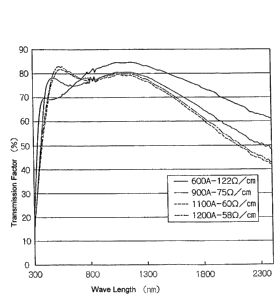
Application Example 67
A transparent laminated film was produced in a film-forming chamber by forming
an ITO-type transparent layer on the surface of the film obtained in
Application Example
1.
More specifically, the layer was formed by RF sputtering using ITO as a
target.
The chamber was evacuated, concentration of oxygen in the chamber was adjusted
to
2x 10~ Torr
RF power was set to 500 W, the
mm temperature was mamtalned at 6U"C;, and the ITO layer was formed.
CA 02488091 2004-12-O1
17
Thickness was adjusted by changing the time during which the inorganic
compound layer was formed. Transparent laminated films were produced in four
different
types. Resistance of the ITO layer and absorption spectra measured with the
use of a
Shimazu spectrophotometer (Model UV3100PC) were determined in all four
transparent
laminated films. Results of measurement are shown in Fig. 1.
Absorption spectra were measured for the second time by the same instrument
a$er heating of the film for 2 hours at 150°C. The results did not show
any changes in
the spectra.
The obtained laminated films were immersed for 2 hours in boiling water, but
this
did not cause peeling of the inorganic layer. Observations did not reveal any
striking
changes in appearance or absorption spectra even after heating the film for 16
hours at
200°C.
A transparent laminated film coated with an ITO layer was immersed into a 6N
nitric acid. The ITO layer was removed, so that the transparent layer made
from the
cross-linked polysiloxane film was exposed. However, no changes were observed
in the
transparent layer, at least in the spectrum of the infrared range measured by
an infrared
spectrophotometer. Tensile strength of the substrate also remained unchanged.
This
indicates to the fact that after the processes of the ITO layer formation and
etching the
transparent layer remains the same as prior to these processes. Thus it can be
assumed
that electrode patterns also can be formed in the laminated film of the
invention.
Application Example 7
A transparent laminated film was produced in a f lm-forming chamber by forming
a thin conductive layer of metal on the film obtained in Application Example
1.
More specifically, the layer was formed by sputtering using gold as a target.
The
chamber was evacuated, concentration of argon in the chamber was adjusted to
the
partial argon pressure of 1.3 mbar, and a thin film of gold was formed at 500
V voltage
and 8 mA current.
The obtained gold filin was sputtered with the use of argon, and an elemental
analysis was conducted with use of X-ray photoelectron spectroscopy (XPS) for
the
material on the interface between the thin gold film and the cross-linked
polysiloxane
film in contact the aforementioned film. Signals 4f (84.8 eV) corresponding to
electrons
of gold were negligibly small, while signals Si2p, C 1 s, and O 1 s
corresponding to
electrons of polysiloxane are shown below in Table 1.
Table 1
Si2 Eb I C1 sEb I __ O1 sEb I
112.8 SS 281.3 39 532.1 164
CA 02488091 2004-12-O1
18
The obtained data and the waveform peaks were the same as prior to vapor
deposition of the layer.
Application Example 8
The film obtained in Application Example 1 was secured to a substrate in the
JEOL (JFC1100) chamber of the sputtering apparatus; pressure in the chamber
was
reduced to 10-6 Torr, the chamber was filled with argon at 10-4 Ton, and then
gold was
applied by sputtering at 800V and 8 mA. As a result, a thin gold layer having
a thickness
of about 100 nm was formed on the film. XPS analysis of the gold layer did not
reveal
peaks other than those corresponding to gold. Immersion of the gold-coated
film for 2
hours in hot water at 90°C did not cause peeling of the coating.
Commercial Applicability
Because of its superior physical and mechanical properties, the polysiloxane
film
of the present invention is self supporting and can be used as a substrate-
independent
film. In addition, because it is cross-linked, the polysiloxane film of the
present
invention exhibits high heat endurance even when heat endurance-imparting
additives are
not used.
In addition, the polysiloxane filin of the present invention is transparent in
the
visible range and exhibits low birefringence. Another superior characteristic
it possesses
is that its optical transmissivity exhibits no polarization dependence. For
this reason, it is
particularly suitable for applications requiring properties such as optical
transparency,
and, moreover, has excellent optical characteristics suitable for both
polarized light and
coherent light. Furthermore, by taking advantage of its transparency over a
wide range of
wavelengths, it can be used in wavelength filters and other optical elements.
In the polysiloxane film of the present invention, the unsaturated aliphatic
hydrocarbon groups of the polysiloxane of aforementioned average structural
formula (1)
are consumed in the process of crosslinking and, as a result, the film does
not absorb UV
light and exhibits high stability to oxygen. Therefore, the polysiloxane film
of the
present invention can be subjected to film-forming treatment in the gas phase
as well.
In general, when a metal oxide thin layer is formed on a film, it is necessary
to
perform high energy treatment, such as sputtering, in an oxygen-containing
environment,
and during such treatment the oxygen is often excited and activated.
Therefore, the film
has to possess high stability to active oxygen, and the polysiloxane film of
the present
invention is stable even under such film-forming conditions. Consequently, the
polysiloxane film of the present invention can be used in optoelectronic
elements, for
instance, as a transparent electrode substrate film.
In addition, even when no additives are used, the film is highly heat-
resistant and
exhibits high resistance to dielectric breakdown, which is an inherent
characteristic of
cross-linked polysiloxane; for this reason, the polysiloxane film of the
present invention
CA 02488091 2004-12-O1
19
can be used in electronics materials requiring high insulating properties,
such as, for
instance, capacitor films, etc.
The polysiloxane film that is structured as a laminated film of the present
invention is permeable not only to light in a visible wavelength range but
also to rays in
ranges from near-ultraviolet to near-infrared. Birefringence through the film
is either
absent or extremely small. 'Therefore, when inorganic layers of the laminated
films of the
invention are used as transparent electrode materials, they may be included
into the
structure of electroluminescence displays, liquid-crystal displays, or similar
thin-type
displays as voltage-receiving electrodes.
Furthermore, the laminated films of the invention can be used as various
filters, reflecting plates, or similar film-type optical elements. By
adjusting resistance of
the inorganic layer, it is possible to utilize the aforementioned films as
electric-charge
removers, electromagnetic shields, etc.
Since the transparent layer of the laminated film of the invention shows high
stability against chemical treatment, the laminated film is suitable for the
formation of
various electrode patterns by removing portions of the inorganic substance
layer by
various etching processes.