Note: Descriptions are shown in the official language in which they were submitted.
CA 02488232 2004-12-02
WO 03/103053 PCT/US03/17362
FABRY-PEROT LASER WITH WAVELENGTH CONTROL
FIELD OF THE INVENTION
The invention is directed to semiconductor lasers with a high side-mode-
suppression ratio and narrow-linewidth for telecommunications applications,
and
more particularly to a Fabry-Perot semiconductor laser that can be post-
processed
into such a device at the wafer level, i.e. before the wafer is separated into
individual
dies by cleaving/dicing.
BACKGROUND OF THE INVENTION
Fabry-Perot (FP) lasers have multiple lasing modes within the envelope of the
gain spectrum, with the modes being separated by the Free Spectral Range
(FSR),
which is determined by the length of the laser cavity between facets and the
effective
refractive index and the dispersion of the active layer. FP lasers are used
today in
short-reach (typically Local Area or Wide Area Networks) applications, where
their
relatively large effective linewidth due to multiple lasing modes around the
nominal
emission wavelength can be tolerated. However, their large linewidth can cause
2o intersymbol interference due to the cumulative effects with distance of the
optical
fiber's chromatic dispersion, thus precluding their use over longer
transmission
CA 02488232 2004-12-02
WO 03/103053 PCT/US03/17362
distances, for example, in Metropolitan Area (MA) and Long Haul (LH) networks.
A
large linewidth can also cause crosstallc problems (or conversely, channel
spacing
limitations) when the channel spacing in DWDM networks is decreased.
Typically,
spans in MA and LH networks require the use of single-mode narrow-linewidth
laser
diodes such as Distributed Feedback (DFB) lasers. DFBs have a grating
extending
along or close to the active layer, and tend to lase in a single mode and have
both a
high side-mode-suppression ratio (SMSR) and a narrow linewidth. However, the
complex etch and regrowth processes required to write the grating and
passivate
afterwards before continuing to lay down the upper device layers make DFBs
very
io expensive to manufacture compared to FP lasers.
Attempts have been reported in the past for transforming a FP laser into a
quasi-
single-mode laser by post-growth processing.
WO Ol/18924A1 discloses forming a two-dimensional pattern of etched recesses
outside the waveguide region of a semiconductor laser, thereby changing the
effective refractive index of the waveguide near the holes. However, the
effective
index contrast is low and, compared to the technique disclosed herein, the
number of
features has to be increased by about two orders of magnitude to stabilize
single-
mode operation.
Another approach for forcing a FP laser into single-mode operation is
described
2o by Kozlowslci et al. in IEEE Photonics Technology Letters Vol. 8, No. 6,
pp. 755-7,
1996. Recesses that extend as far down as the upper edge of the active layer
of a FP
laser are formed in order to suppress certain modes. However, the design of
Kozlowski et al. requires that the recesses be located at an integer fraction
of the laser
length L, e.g. L/2, L/4 or L/8, from a laser facet. Because the recesses are
preferably
CA 02488232 2004-12-02
WO 03/103053 PCT/US03/17362
formed before the wafer is cleaved into laser dies and due to the uncertainty
of
several microns in the as-cleaved length of any given laser die, this
technique can
only be performed with accuracy on discrete, mounted laser devices, the
lengths of
which have been measured. The process is therefore difficult to realize in
practical
applications and expensive to implement.
Another approach has been proposed by DeChiaro in J. Lightwave Technol.,
Vol. 9, No. 8, pp. 975-986, Aug. 1991, wherein absorbing regions are
introduced at
appropriate locations along the optical axis of the device. The absorption
regions are
also placed at sites that are predetermined integer fractions of the laser
length which
1o again requires that the length of the FP laser be accurately known.
It would therefore be desirable to produce a quasi-single-mode laser with a
high
SMSR from a conventional FP laser without prior definition of the cavity
length of
the FP laser. It would further be desirable to produce such lasers
economically using
standard laser processing tools at the wafer level, i.e., before
dicing/cleaving the
1s wafer into individual devices.
SUn~VIARY OF THE INVENTION
The systems and methods described herein include systems and methods that
control the lasing modes of a Fabry-Perot (FP) laser, and more particularly to
a
2o semiconductor FP laser that can be post-processed into such device at the
wafer
level, i.e. before the wafer is separated into individual laser dies by
cleaving/dicing.
According to one aspect of the invention, a laser device includes a laser
cavity
having an optical waveguide and facets defining first lasing modes and a sub-
cavity
formed within the laser cavity. The sub-cavity has a predetermined length and
is
CA 02488232 2004-12-02
WO 03/103053 PCT/US03/17362
located between the facets, wherein the predetermined sub-cavity length
defines
second lasing modes having a free spectral range (FSR) that is greater than a
FSR of
the first lasing modes. The device further includes a plurality of contrast
elements
having predetermined inter-element separations and predetermined spacings
relative
to the sub-cavity, wherein the contrast elements interact with the optical
waveguide
and form an aperiodic grating. The inter-element separations and the spacings
produce a filtering function of the aperiodic grating for optical radiation
propagating
in the waveguide.
The small sub-cavity is designed to expand the mode spacing of the FP laser.
In
1o addition, an aperiodic grating filter in the form of contrast elements
(typically fewer
than 20) is applied along the waveguide, i.e., between the facets and inside
and/or
outside the sub-cavity, that has a transmission passband at the desired lasing
wavelength and substantially a stop-band over a range of adjacent frequencies
on
both sides of the desired lasing wavelength. The contrast elements can be
formed in
15 or adjacent to the waveguide layer of the laser.
Embodiments of the invention can include one or more of the following
features.
The sub-cavity length can be defined by at least two discontinuities, such as
trenches
and/or cleaves, extending into said optical waveguide. The waveguide can
include an
upper cladding layer, wherein said contrast elements comprise regions having
an
20 index of refraction that is different from an index of refraction of the
upper cladding
layer and/or of the waveguide. The filtering function can cause the laser
device to
emit laser radiation with at least one defined mode. Preferably, the emitted
laser
radiation can be single-mode. A contact layer can be disposed at least over
the length
of the sub-cavity, but may also be disposed over the waveguide region located
CA 02488232 2004-12-02
WO 03/103053 PCT/US03/17362
between the facets. The facets can be anti-reflection coated.
The laser device can also be implemented as a surface-emitting laser by
forming at least one of said facets as an inclined facet that directs the
optical
radiation propagating in the waveguide in a direction substantially normal to
the
waveguide. Alternatively, at least one of said facets can be oriented
perpendicular to
the waveguide and located opposite to a reflecting facet that directs the
optical
radiation propagating in the waveguide in a direction substantially normal to
the
waveguide.
According to another aspect of the invention, a method for producing optical
1o radiation with a desired mode structure includes producing an optical
waveguide
capable of propagating the optical radiation; forming in the optical waveguide
a sub-
cavity with a predetermined length, the sub-cavity producing a sub-cavity mode
structure that overlaps with the desired mode structure; and forming along the
optical
waveguide an aperiodic filter having contrast elements, the aperiodic filter
filtering
1s the sub-cavity mode structure to generate the desired mode structure. The
optical
filter is generated by defining a cost function representing a goodness of fit
between
the desired mode structure and an actual spectral response of the filter;
assigning to
each contrast element of the aperiodic filter at least one characteristic
attribute;
generating an initial aiTangement of the contrast elements along the optical
2o waveguide; and iteratively modifying at least one characteristic attribute
of at least
one of the contrast elements and computing for each iteration a cost function.
If the
computed cost function for an iteration is less than a predetermined cost
function
value, a corresponding arrangement of the contrast elements is selected as an
optimal
arrangement of the contrast elements to provide the desired mode structure.
CA 02488232 2004-12-02
WO 03/103053 PCT/US03/17362
Embodiments can include one or more of the following features. The optimal
arrangement of the contrast elements can define a spatial layout of said
contrast
elements relative to one another and relative to said sub-cavity. Facet
locations can
be defined along said optical waveguide, said facet locations defining Fabry-
Perot
s modes, wherein said sub-cavity and said optimally arranged contrast elements
are
located between said facet locations. The distance between said facet
locations, on
one hand, and said sub-cavity and said optimally arranged contrast elements,
on the
other hand, need only be known approximately. The characteristic attributes of
the
contrast element can be a refractive index, a physical dimension, such as a
width
1o and/or height, or a spacing between adjacent contrast elements.
Further features and advantages of the present invention will be apparent from
the following description of preferred embodiments and from the claims.
Brief Description of the Drawings
15 The following figures depict certain illustrative embodiments of the
invention in
which like reference numerals refer to like elements. These depicted
embodiments
are to be understood as illustrative of the invention and not as limiting in
any way.
FIG. 1 shows schematically a conventional Fabry-Perot (FP) laser;
FIG. 2 shows schematically above-threshold laser modes of the FP laser of FIG.
1;
2o FIG. 3 shows schematically the laser of FIG. 1 with a formed sub-cavity;
FIG. 4 shows schematically laser modes of the FP laser cavity with the sub-
cavity
of FIG. 3;
FIG. 5 shows schematically an aperiodic grating formed in the laser structure
of
FIG. 3;
6
CA 02488232 2004-12-02
WO 03/103053 PCT/US03/17362
FIG. 6 shows schematically laser modes of the FP laser cavity of FIG. 5;
FIG. 7 is a flowchart of a process for computing an optimized aperiodic
grating
structure;
FIG. 8 shows an embodiment of a vertically emitting laser with a horizontal
waveguide; and
FIG. 9 shows another embodiment of a vertically emitting laser with a
horizontal
waveguide.
Detailed Description of Certain Illustrated Embodiments
1o The systems and methods described herein are directed to a modified FP
laser
that produces quasi-single-mode laser emission. In particular, the modified FP
laser
described herein can be fabricated by post-processing of standard FP lasers at
the
wafer level under relaxed tolerances for the subsequent cleaving process.
Referring now to FIG. 1, a conventional FP laser cavity 10 is defined by two
facets 12, 14 that can be cleaved, etched, milled or prepared by any other
method
known in the art. The facets 12, 14 are typically coated to control their
reflectivity
and prevent degradation when exposed to ambient atmosphere. Laser radiation
propagates in the waveguide 16 which is formed of a material having a higher
index
of refraction than the adjacent cladding layers 15, 17.
The exemplary FP laser of FIG 1 has a length of 400 pm and can have
multiple lasing modes within the envelope of the gain spectrum, as illustrated
in the
simulated spectral emission of laser 10 in FIG. 2. The mode spacing is
determined by
the Free Spectral Range (FSR), which is a function of the length of the laser
cavity
between facets and the effective refractive index (and its dispersion) of the
active
7
CA 02488232 2004-12-02
WO 03/103053 PCT/US03/17362
layer. In this example, if the refractive index is assumed to be 3.3, then
neglecting
dispersion the FSR is 113.5 GHz, or 0.91 nm. FP lasers are poorly suited for
applications where a stable laser emission with narrow linewidth is required,
such as
for DWDM optical telecommunication applications.
The mode spacing of an FP laser is inversely proportional to the cavity
length. A shorter cavity FP laser will therefore have a smaller number of
cavity
modes within the gain curve. In an extreme case, a VCSEL (vertical cavity
surface
emitting laser) may only support a single mode within its gain curve and will
hence
operate single mode.
to Referring now to FIG. 3, an exemplary FP laser 30 has formed therein, for
example, by cleaving (similar to a cleaved-coupled-cavity laser known in the
art,
with cleaves 33, 35 typically extending through the wafer), by deep etching or
ion
milling using a focused ion beam (FIB) at least one slot or recess 32, 34 that
can
extend into the waveguide. Recesses 32 and 34 form a shorter cavity with a
reduced
1s number of laser modes. The cleaved facets 12, 14 of laser 30 can be
antireflection-
coated, so that the mode spacing is predominantly determined by the optical
distance
between the recesses 32 and 34. A simulated lasing spectrum of an exemplary
semiconductor laser having a length of 400 ~m and a spacing between the
recesses
32, 34 of 75 ~m is shown in FIG. 4. The mode separation (i.e. FSR) is now
2o increased to approximately 605.7 GHz or ~4.8 nm. Unlike prior art modified
FP
lasers, wherein the recesses are placed along the waveguide at locations that
are an
exact fraction of the cavity length defined by the distance between the facets
12 and
14, the emission spectrum of laser 30 is essentially unaffected by the
distance of the
recesses 32, 34 from the cleaved facets 12, 14.
CA 02488232 2004-12-02
WO 03/103053 PCT/US03/17362
The length of the sub-cavity between the recesses 32, 34 is preferably
selected such that one mode coincides with a desired single-line spectral
response,
with the other supported modes selected so as not to coincide with other
wavelength
channels (e.g. ITU defined) in use in the communications system in which the
laser is
to be deployed.
The laser 30 as well as the other laser structures 10, 50 described herein are
typically electrically pumped. For this purpose, contact layers 36 and 38 are
applied
to opposite sides of the laser structures 10, 30, 50. The contact layers 36,
38 may
extend over the entire cavity length between facets 12, 14 or only over a
specified
to portion of the cavity. Lasers having, for example, unpumped end regions
proximate
to the facets 12, 14 are known in the art.
FIG. 4 shows a simulated emission spectrum of the FP laser 30 of FIG. 3 with
the recesses 32, 34 formed in the waveguide 16. The spectrum is still
multimode.
However, the modes are spaced farther apart than those of laser 10, as
determined by
1s the optical length of the waveguide between the recesses 32, 34.
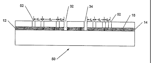
As illustrated in FIG. 5, in a second step of the fabrication process of the
modified FP laser, a small number of, in the example given a total of six,
"contrast"
elements 52 that form an aperiodic grating structure are added to the laser
structure
30 of FIG. 3. The aperiodic grating structure can be formed, for example, by
2o implanting ions to alter the doping level or composition near the waveguide
16 using
FIB, lithography and/or diffusion. Optimal spacings dl, d2, d5, d6 between the
contrast elements 52 themselves as well as spacings d3 and d4 between a
contrast
element 52 and a respective recess 32, 34 are calculated using an "annealing"
method
with a random seed. Details of this method will be described in detail below.
The
25 calculated values are dl = 46.88, d~ = 90.63, d3 = 34.38, dø =46.88, ds =50
and d6
CA 02488232 2004-12-02
WO 03/103053 PCT/US03/17362
=6.25 ~.m, respectively. It should be emphasized that the relative lengths d;
are
critical, while the distances between the contrast elements 52 and AR-coated
facets
12, 16 are not important and need not be tightly controlled. The aperiodic
grating
operates collectively to further filter the cavity modes produced by the
recesses 32,
s 34.
Modes of the exemplary aperiodic grating are depicted in the diagram of FIG.
6. The cavity with the trenches and the grating elements are simulated using a
simplified laser model which takes into consideration gain without full
reference to
rate equations. The gain spectrum is represented in this model by an enlarged
spectral
1o width consistent with the objective of single-mode high-SMSR lasing over a
wide
temperature range, utilizing a simple device packaging scheme without
temperature
control, i.e. 'uncooled'.. The exemplary modified Fabry-Perot laser is
designed using
a software design program that can be readily written in a high-level language
such
as MATLABTM, available from MathWorlcs Inc., Naticlc, MA.
1s The aperiodic grating can be designed for the device 30 by starting with a
simulated grating having grating elements, i.e., the "contrast" elements, with
initial
positions along the waveguide 16 defined by a random seed value. Several
constraints may be applied to the grating elements, such as a minimum
manufacturable feature size, a desired maximum number of grating elements,
etc.
?o The grating lines do not define a plurality of coupled cavities within the
overall laser
cavity to increase mode spacing, but rather represent a filter that has a
transmission
passband at the desired lasing wavelength and substantially a stop-band over a
range
of adjacent frequencies on both sides of the desired lasing wavelength. Thus,
consistent with the desired spectral response, an arbitrary number of
sidemodes
2s adjacent to the lasing wavelength may be suppressed.
CA 02488232 2004-12-02
WO 03/103053 PCT/US03/17362
FIG. 7 is a schematic flow diagram of an optimization algorithm suitable for
carrying out the invention. An optimization algorithm of this type is commonly
referred to as simulated annealing.
Simulated annealing is a process which mimics actual annealing of a material
by heat treatment. The material is hereby heated up and then slowly cooled
down.
Previously displaced atoms will then move into their respective equilibrium
positions, and dislocations and defects will be largely eliminated.
In simulated annealing, a cost-function takes the place of the potential
energy
of an atom. The aim of the process is to locate a global minimum in cost
space, by
1o randomly "hopping" solutions around (a "hot" system) and then gradually
"cooling"
the system, thereby reducing the size of the random hops. If the cooling rate
is
chosen correctly, the solution will hop into the global minimum while the
system is
hot and be kept there as the system cools.
A flowchart of the optimization process 700 is depicted in FIG. 7. The
15 process 700 starts with step 702 by setting an index i=0 and defining a
target filtering
function T (~,) which represents, for example, a desired spectral output as a
function
of the wavelength ~, of the exemplary laser structure 10 or 30. A random seed
value
representing a possible grating structure within selected confines, such as
refractive
index step, manufacturable feature size, etc., is selected, generating an
initial,
2o typically aperiodic, real space grating structure Ho (x), step 704, wherein
x represents
a coordinate along the length of waveguide 16. An initial simulated annealing
"temperature" To, a cooling rate oc, and a limit N for the number of
iterations can
also be assigned at this time, step 706. In step 708, the Fourier Transform
(FT) of the
initial real space grating structure Ho (x) is calculated, giving an initial
filtering
25 function ho (~,) = FT [Ho (x)].
il
CA 02488232 2004-12-02
WO 03/103053 PCT/US03/17362
A cost function Co = ~ ~T ~~.) - lao (~,))z is calculated over the spectral
range
of interest, step 710. As can be seen, the cost function Co will decrease when
the fit
between the target filtering function and the calculated filtering function
(FT of the
real space grating structure) improves. To test if the cost function can be
lowered, the
s index i is increased by l, step 712, and a characteristic feature of a
randomly selected
element in the grating structure Ho (x) is modified to produce a new grating,
Hl (x),
step 714. The characteristic feature can be a refractive index of an element,
a width
and/or height of an element, and/or a spacing between elements or groups of
elements. In step 716, the FT of the modified real space grating H; (x) is
calculated,
to yielding a new filtering function h; (~,) = FT [H; (x)]. A new cost
function
C; _ ~ ~T(~,)- h; (~,))Z is calculated, step 718, and compared with the cost
function
C;-1 for the previous grating structure, i.e. initially with Co for the
initial grating Ho
(x). If it is determined in step 720 that the new cost function C; is lower
than the cost
function C;_l, then the new grating is accepted as an improved structure and
used as a
15 basis for subsequent iterations, step 722. If the maximum number of
iterations N has
not been reached, as determined in step 724, then the index i is incremented
by 1,
step 712, and the process returns to step 714.
Conversely, if it is determined in step 720 that the new cost function C; is >
C;_l, then a random number R between 0 and 1 is computed, step 726, and it is
2o checked in step 728 if exp~ IC; -C;_,I lT)> R, in which case the new
grating is
accepted and the process 700 returns to step 722. However, if the difference
between
C; and C;_1 is such that exp~ (C; - C;_1 I / T) 5 R , then the new grating H;
(x) is
rejected and the element or feature previously changed in step 714 is returned
to its
12
CA 02488232 2004-12-02
WO 03/103053 PCT/US03/17362
previous state and the process returns to step 714 via the steps 724 and 712
described
above.
If the limit N for the number of iterations has been reached, as determined in
step 724, the process 700 checks in step 732 if the Fourier transform hN (~,)
= FT [HN
(x)] of the grating HN (x) is sufficiently close to the target function T(~.),
for example,
by computing the cost function CN = ~ (T~~,)-hN (~,))2, and should therefore
be
accepted as an "optimized" structure, step 734. Those skilled in the art will,
of
course, appreciate that this "optimized" structure may be a locally, but not
necessarily a globally optimized structure, which is mathematically difficult
to obtain
to unless the entire search space is investigated.
If it is determined in step 732 that hN (7~) is not sufficiently close to the
target
function T(7~), then the annealing temperature T is multiplied by a
predetermined
factor a<1, i.e., the system is "cooled down", step 736, and the loop counter
i is set
again to zero, step 738. The process 700 then return to step 714 for another
random
15 grating change.
The cooling rate a is typically lcept constant throughout the annealing
process. If h;(~,) does not change after executing additional loops, the
process is
stopped (not shown) as this may be a sign that the temperatur a is too low for
further
2o changes.
Practical limitations of the fabrication process may impose constraints on the
parameters of the design model. For example, certain dimensions of the grating
elements and spacing between the grating elements may be dictated by the
feature
sizes achievable with photolithography and/or focused ion beam milling.
13
CA 02488232 2004-12-02
WO 03/103053 PCT/US03/17362
Additionally, the grating lines can also have different shapes, as long as
these shapes
can be adequately and efficiently modeled and manufactured, including but not
limited to V-shaped features and cylindrical 'holes'. As mentioned above, the
model
assumes that following dicing/cleaving the cleaved laser facets will be
antireflection
coated for the wavelength range of operation. The laser performance is
substantially
independent of the absolute position of the grating elements relative to the
laser
facets, and also of the laser facet reflection phase. Instead, the performance
depends
on the relative positions of the grating elements along the waveguide 16.
The modified FP laser can also be designed to operate as a surface emitting
1o laser. In this way, the basic operation of the laser can be tested by
applying electrical
probes at the wafer level, i.e. before cleave/dice and mounting etc. Lasers
can then
simply be mapped and those lasers that do not meet established performance
criteria
can be marked and discarded at time of cleave/dicing. This can represent a
considerable cost saving compared with the alternative standard methods for
edge-
emitting lasers, in which individual lasers have to be cleaved, diced and
mounted
prior to testing even their basic performance.
FIG. 8 shows schematically a surface-emitting laser 80 with a horizontal-
cavity laser using a turning mirror 82. Optical radiation propagating in the
waveguide
16 exits the waveguide through facet 84 and is reflected by the turning mirror
82.
2o The angle of the turning mirror 82 relative to the waveguide 16 can be
selected so
that emitted beam B has a predetermined direction relative to the wafer
surface.
Facets 84 and turning mirror 82 can be formed on one end of the optical
cavity, as
indicated in FIG. 8, or on both ends (not shown). To achieve high
reflectivity, the
turning mirror 82 is preferably coated with a dielectric or metallic high-
reflectivity
~5 coating. Alternatively, as depicted in FIG. 9, a single trench 92 can be
formed that
14
CA 02488232 2004-12-02
WO 03/103053 PCT/US03/17362
extends beyond the active region at an angle a, relative to the laser chip
surface. The
optical radiation propagating in the waveguide is totally internally reflected
at the
interface 94 at an angle 2a relative to the wafer surface.
For a surface-emitting laser emitting normal to the wafer surface, the angle
oc is 45°.
For salve of clarity, the surface-emitting structures of FIGS. 8 and 9 are
illustrated for
a conventional FP laser 10, and it will be understood that the surface-
emitting
structures can be readily employed with the laser devices 30 and 50 of the
invention.
The laser device structure, such as the structure 10 of FIG. l, can be
produced
by a conventional epitaxial process, such as MBE or MOCVD. Trenches 32, 34 can
1o be milled through an applied top contact layer and upper cladding layers
into the
active layer to define the short cavity (FIG. 1), for example, by FIB milling
using a
Focused Ion Beam (FIB) apparatus, such as Model DB 2358251 manufactured by
FEI Corp, Hillsboro, Oregon. Other processes for forming the trenches or other
suitable discontinuities can also be used, such as electron beam lithography
followed
by a robust etching technique compatible with high aspect ratio deep etching
that
preserves good sidewall smoothness, for example, ECR/ICP etching using
chlorine
chemistry. Alternatively, the sub-cavities can also be produced by cleaving
through
the wafer. The etched sidewalls should be smooth to limit scattering in the
laser
cavity.
The upper surface can be passivated, for example, by depositing or spin-
coating a suitable polymer material of suitable viscosity or a glass.
Photoresist could
be used to delineate openings for forming the elements/features of the
aperiodic
grating structure. Other materials, for example, a dielectric material such as
Si02 or
Si3N~, can also be deposited over the surface and into the grating trenches,
consistent
CA 02488232 2004-12-02
WO 03/103053 PCT/US03/17362
with the design being based on the implied index contrast, and consistent with
minimal thermal strain effects.
The contrast elements ~of the aperiodic grating can be defined by aligning a
photomaslc that includes the features of the aperiodic grating with the
trenches of the
sub-cavity. Photolithographic processes known in the art can then be employed
to
define openings in the top contact or cladding layer to form the contrast
elements, for
example, by impurity diffusion, ion milling, chemical etching, and the like.
It should
be noted that the contrast elements do not have to project into the waveguide
layer,
but need only disturb the refractive index of the waveguide region.
Accordingly,
1o design criteria similar to those employed with DFB and DBR laser structures
can be
adopted.. In an exemplary embodiment utilizing an FIB-based process on a
buried
heterostructure, the contrast elements are created as follows: the
metallization of the
top contact layer is removed to create a window by setting the beam current
sufficiently high to mill through the contact layer. The beam current can then
be
reduced to a level consistent with ion implantation through the opened window.
A
calibrated FIB implantation procedure, followed by an optional annealing step,
creates contrast elements of the desired index contrast by
implantation/diffusion of
gallium ions into the upper cladding layer. Those skilled in the art will
appreciate that
windows can also be defined in the top contact layer by lithography for a
subsequent
2o wafer-level impurity diffusion, which may be preferable over ion
implantation
depending on the desired index contrast, the number of contrast features, and
global
calculations of throughput and process cost per device yielded.
While the invention has been disclosed in connection with the preferred
embodiments shown and described in detail, various modifications and
~5 improvements thereon will become readily apparent to those skilled in the
art. For
16
CA 02488232 2004-12-02
WO 03/103053 PCT/US03/17362
example, the laser device can be an optically pumped semiconductor laser, an
optically pumped solid state laser having a waveguide region or an optically
pumped
fiber laser. The device can also be made of a bull: material, such as a Nd:YAG
crystal, with the trenches and aperiodic grating structure including
discontinuities in
the refractive index produced, for example, by mechanical means, impurity
diffusion
and the like. Accordingly, the spirit and scope of the present invention is to
be
limited only by the following claims.
17