Note: Descriptions are shown in the official language in which they were submitted.
CA 02488408 2004-12-02
WO 03/107390 PCT/EP03/06125
Lighting Element with Luminescent Surface
The present invention concerns a lighting element with a luminescent surface
containing a
layer system with a base electrode layer made from an electrically conductive
material and
directly or indirectly arranged thereon a translucent dielectric layer with a
front surface and a
back surface facing the base electrode, where the dielectric layer contains an
arrangement of
pores extending between the front and back surfaces and the pores are open to
the front
surface, and emitter rods of an electrically conductive material are arranged
within pores,
where the emitter rods are connected to the base electrode in an electrically
conductive
manner, and opposite the emitter rods is a translucent counter-electrode of an
electrically
1o conductive material, and between the emitter rods and the counter-electrode
is arranged a
luminescent material. The invention also concerns the manufacturing and the
use of the
lighting element in accordance with the invention.
Luminescent materials or substances, i.e. solid, liquid or gaseous materials
which can be
stimulated to emit light, have been known for some time for the manufacture of
lighting ele-
ments. Luminescent materials, also known as luminophores or fluorescent
substances, can
be stimulated to emit light by for example electromagnetic waves, such as
ultraviolet (UV)
radiation or visible light, by electric fields, by electron beams or by ions,
e.g. ionised gas at-
oms or molecules. Luminescence can also include phosphorescence or
fluorescence.
Luminescence achieved through the targeted, i.e, addressed, stimulation of
individual light
2o points is used for example in screens, whereas the unaddressed stimulation
of a luminescent
substance is used in lighting appliances.
In computer and TV screens for example, a targeted stimulation of individual
luminescent
points occurs through electron beams. In discharge lamps, such as fluorescent
tubes, a lu-
minescent substance is stimulated to emit light by way of UV radiation.
Generally, gases are
here used which emit UV radiation through stimulation by electron beams.
Moreover the lu-
minescent substance of discharge lamps can also be stimulated directly by
ionised gas at-
oms or molecules.
'For certain applications it is advantageous to have flat lighting elements
with a total thickness
as thin as possible and which can also be manufactured easily and cheaply in
large quanti-
ties.
For example, flat lighting elements are known which are based on the principle
of cold cath-
ode field emission. These are distinguished by a cold cathode, which under the
effect of an
external electric field emits electrons which in turn stimulate a luminophore
to emit light. High
CA 02488408 2004-12-02
WO 03/107390 PCT/EP03/06125
-2-
emission currents depend on high field strength which in turn depends on a
high field. That
can be achieved along with a low potential difference by minimising the
distance between the
emitters and the Anode.
Therefore in order to keep the operating voltage applied to the cathodes as
low as possible
whilst at the same time reaching the necessary high electrical field
strengths, the cathode
surfaces are provided with fine cathode points. An anode is placed opposite
the cathode and
absorbs the electrons emitted by the cathode points. As above mentioned the
distance be-
tween the anode and the cathode points is minimised to achieve a high field.
There are various procedures according to which cathode surfaces can be
produced with a
1o multiplicity of cathode points. EP 0 351 110 for example describes a
procedure for the
manufacture of cold cathode emitter surfaces where an aluminium oxide surface
is provided
with numerous elongated pores arranged substantially orthogonal to the main
surface of the
aluminium oxide layer, the pores are filled with a metal, at least a part of
this aluminium oxide
layer is removed leaving a surface with exposed cathode points that are no
longer sur
rounded by the aluminium oxide layer.
WO 96/06443 describes a targeted cold cathode field emission arrangement for
displays and
screens. A porous membrane of aluminium oxide is applied to a layering system
with an ad-
dressable cathode. The pores of the membrane are filled with a conductive
metal which
forms emitter cathodes, where the emitter cathodes are conductively connected
to the target
2o cathodes and their front points end at the level of the front surface of
the dielectric mem-
brane. The anode is integrated into the phosphorus screen, which is arranged
at a distance
from the cathode.
Previously known flat lighting elements which work on the principle of
luminescence gener-
ally have a relatively large total thickness. In addition, they are often
expensive and complex
to manufacture. In addition, in known flat lighting elements, the dimensional
stability of the
distance between the anode and the cathode is often too small, which leads to
a lower and
uneven light emission.
The purpose of this invention is therefore to propose a lighting element with
a light-emitting
surface based on the principle of luminescence, which has a small total
thickness and is
3o easy and cheap to manufacture.
In accordance with this invention, this is resolved in that the counter-
electrode is part of the
layer system and is a layer covering the pore cavities and arranged directly
or indirectly on
the front surface of the dielectric layer, and the luminescent material is
arranged between the
emitter rods and the layer of counter-electrode, and the dielectric layer is a
spacer, which
separates the base electrode and the counter-electrode.
CA 02488408 2004-12-02
WO 03/107390 PCT/EP03/06125
-3-
The term "light" in this document means the electromagnetic radiation of the
visible (to the
human eye) spectrum and radiation from the infrared and ultraviolet ranges
adjacent to the
visible spectrum. Moreover the term "light" according this specification shall
also encompass
electromagnetic radiation of the soft X-ray spectrum.
Emitter rods are the electron-emitting, thread-like, wire-like or cone-like
deposits in the pores.
The emitter rods suitably lie completely in the pore cavity.
In a embodiment (A) according the invention, the luminescent material is
arranged directly or
indirectly as a layer covering the pore openings on the front surface of the
dielectric layer.
The counter-electrode is arranged directly or indirectly on the exposed
surface of the lumi-
1o nescent layer. According this embodiment the emitter rods may end at the
pore openings.
In a embodiment (B) according the invention, luminescent material is arranged
in the pore
cavity between the emitter rods and the pore openings. The luminescent
particles can be
deposited in the free pore cavity and fill this partly or fully.
In addition, the luminophore can be arranged partly or fully as a layer on the
exposed surface
of the pore inner walls, forming or retaining a preferably central pore
cavity. The counter-
electrode here is arranged directly or indirectly on the front surface of the
dielectric layer. The
luminophore can be arranged exclusively on the exposed surface of the pore
inner walls
between the pore openings and the emitter rods. In this case the luminophore
is preferably
deposited after depositing the emitter rods. Further the luminophore may also
be deposited
2o before the emitter rods and therefore also covering pore inner wall
sections in the region
where the emitter rods are subsequently deposited.
Optionally embodiment (A) and (B) may also be combined.
The luminescent particles arranged for example as a layer on the front surface
of the dielec-
tric layer have e.g. a size of up to 20 ~,m, preferably up to 10 p,m. If the
luminescent particles
are deposited in the pores, it is preferable to use luminescent particles in
the form of nano-
particles measuring e.g. 100 nm or smaller. In this embodiment the luminescent
particles can
be deposited on the pore walls or in the pores for example by way of an
electrophoresis pro-
cedure.
The luminescent particles can also be deposited on the pore walls in the form
of self-
3o assembled monolayers (SAM), whereby the luminescent particles are attached
as a func-
tional group on the SAM's. Self-assembled monolayers are tightly packed
monolayers
formed through adsorption. SAM's can be constructed e.g. on the basis of
phosphoric acid
ester. "Self-assembled monolayers" are of a thickness of e.g. 1 to 10 nm,
preferably 1 to 5
nm. Further details of the properties and structure of SAM's can be found in
the "Ullmann's
CA 02488408 2004-12-02
WO 03/107390 PCT/EP03/06125
-4-
Encyclopaedia of Industrial Chemistry, 6. Edition, 2001 Electronic Release,
Ch. 1.5.1 ".
The luminescent layer can also consist of "multilayers", which are formed
under controlled
conditions by the sequential adsorption of "self-assembled monolayers".
Correspondingly suitable compounds can be used as luminophores as detailed in
e.g. Ro-
empp, Chemical Lexicon, 10th Edition, 1997, p. 2389-2391. A suitable compound
is e.g.
ZnS. For the manufacture of ZnS layers, the pore cavities can be coated e.g.
with a solution
of ZnSOq.. Once the solution is dry and the pores have been gassed with H2S, a
layer of ZnS
is formed in the pores.
In a further development of the invention a layer-like intermediate electrode
can be arranged
1o directly or indirectly on the front surface of the dielectric layer,
surrounding the pore open-
ings, i.e. not covering these. The intermediate electrode therefore has a
perforated structure.
The intermediate electrode may be applied in embodiment (A) and embodiment (B)
as well.
In the lighting element according to embodiment (A) but with an additional
intermediate elec-
trode, the luminescent layer is arranged directly or indirectly on the layer
of intermediate
electrode and the layer of counter-electrode directly or indirectly on the
luminescent layer,
whereby an isolation layer can be arranged between the luminescent layer and
the counter-
electrode and/or the intermediate electrode.
In the lighting element according to embodiment (B) but with an additional
intermediate elec-
trode, at least one extra dielectric layer is arranged over the intermediate
electrode and the
layer of counter-electrode is arranged on the at least one extra dielectric
layer.
The intermediate electrode is preferably a layer of electrically conductive
and reflective mate-
rial such as metal (e.g. aluminium, silver or titanium) applied e.g. by PVD
(physical vapour
deposition). The layer thickness of the intermediate electrode can be e.g. 20 -
150 nm.
The base electrode can be made from an anodisable metal, i.e. a valve metal
such as mag-
nesium, titanium or aluminium and an alloy thereof. The base electrode is
preferably made
from aluminium or an aluminium alloy and in particular from pure aluminium.
The base elec-
trode can be made e.g. from aluminium with a purity of 95% or higher,
preferably 98.3% or
higher, in particular 99.5% or higher. The base electrode is preferably a
layer formed by a
coating procedure to a substrate. The surface of the base electrode may also
be formed by
3o the substrate itself. The substrate may be made of a flat element, such as
a plate, sheet or
film or of a shaped body. The substrate may be produced by means of e.g. a
rolling, extru-
sion, forging or flow press procedure. The substrate for the base electrode
may also be
made of an extruded profile or a cast product.
The dielectric layer is e.g. a layer or membrane from a translucent metal
oxide, preferably
CA 02488408 2004-12-02
WO 03/107390 PCT/EP03/06125
-5-
aluminium oxide. The dielectric layer is preferably a layer manufactured by
the anodic oxida-
tion of a metal substrate under pore-forming conditions.
The dielectric layer preferably comprises a porous layer, or a porous layer
and where appli-
cable a barrier layer forming the back surface. If a barrier layer is
provided, this suitably has
a thickness which allows a flow of electrons between the base electrode and
the emitter
rods. Therefore the layer thickness is preferably less than 50 nm,
particularly less than 30
nm. The barrier layer itself can also contain inclusions which increase its
conductivity.
Where the pores of the dielectric layer contains in addition to emitters
luminescent material
(embodiment (B)) or a plasma-forming gas (principle (ii), (iii)) then the
dielectric layer for ex-
1o ample has a thickness of greater than 1 p,m and preferably greater than 2
~,m or in particular
greater than 5 p,m and less than 150 p,m, preferably less than 100 p,m and in
particular less
than 70 ~.m.
Where the pores of the dielectric layer contains only emitters and the
luminescent material
covers the pore openings (embodiment (A)), then the dielectric layer has
preferably a lower
thickness as above described. The thickness of the dielectric layer may be
here 20 p,m or
less, preferably, 10 p,m or less and particularly 0,05 to 5 Vim. However the
thickness of the
dielectric layer is preferably determined by the length of the emitter rods
and the preference
for them to extend over nearly all the pore length.
According the current state of technology nano-phosphors as luminescent
material can be
2o produced in a size of 50-100 nm. If these particles are to be introduced
into the pores, then
the pore diameter at the front surface of the dielectric layer are preferably
greater than 50
nm, preferably greater than 100 nm. It may be possible to relax these criteria
where alterna-
tive light-emitting substances or plasma-forming gases are introduced into the
pores.
If the metallic intermediate electrode is to be deposited, e.g. vacuum
deposited, on the di-
electric layer surface, then the amount of deposit is preferably sufficient to
provide an ade-
quately conductive surface film but not so much to seal the pores and block
the path of
emitted electrons. Therefore if an intermediate electrode is applied, e.g. by
means of vacuum
deposition, then the pore diameter at the front surface of the dielectric
layer beneath the in-
termediate electrode is preferably 10 nm or greater, particularly 50 nm or
greater and pref-
3o erably 200 nm or less, particularly 90 nm or less.
The pore diameter at the front surface of the dielectric layer is preferably
10 to 250 nm or
even greater.
The pores are suitably aligned substantially orthogonal to the front surface
of the dielectric
layer. The dielectric layer has for example a pore density of 10$ pores per
cm2 or higher. The
CA 02488408 2004-12-02
WO 03/107390 PCT/EP03/06125
-6_
separation between the emitters is preferably 0,05 - 10 Vim. The dielectric
layer preferably
has a thickness greater than the mean diameter of the pores. The pore
population density
and pore diameters may be made to vary through the dielectric layer thickness.
The dielectric layer also serves as a spacer, which separates the base
electrode and the
counter-electrode. The distance between the base electrode and the counter-
electrode is
therefore relatively small, allowing the operation of the lighting element
with relatively low
electric voltages. In order to reduce power requirements, field emission
should be at a field
strength less than 100 V/p,m, preferably less than 30 V/p,m and particularly
less than 20
V/pm. This defines the separation between the emitter rods and the counter-
electrode or, if
io present, the intermediate electrode.
The pores contain thread-like or wire-like emitter rods which are connected
electrically con-
ductively to the base electrode. If the dielectric layer does not contain a
barrier layer, the
electrical contact between the base electrode and the emitter rods is made
directly.
The emitter rods are made from an electrically conductive material such as
cobalt, nickel or
another suitable metal and are preferably deposited in the pores by means of
electroplating.
The emitter rods are preferably minimised in size and particularly in length.
Thus, the length
of the emitter rods is, on average, preferably less than 10 Vim, particularly
less than 5 ~m and
most preferably less than 1 p,m. If the emitter rods are too large, they will
tend to scatter and
absorb the light produced. Another reason why the emitter rods should be
minimised in
length is to control the uniformity oh their length, which will also
contribute to the uniformity of
light emission.
The emitter rods may contain emitter points at their exposed ends made from
refractory
metal which can also withstand oxidation. The refractory metal can be gold,
molybdenum,
tungsten, palladium, platinum or another metal which is difficult to oxidise.
The emitter rods suitably lie in the pore cavities and under the front surface
of the dielectric
layer. The emitter rods (where applicable with emitter points) preferably
extend over a dis-
tance of less than the pore length. In embodiments of the invention where the
dielectric layer
only contains emitters and the light-emitting substance is beyond its front
surface (embodi-
ment (A)), then the emitter rods preferably extend very close to the front
surface, but pref-
3o erably no closer than two pore diameters.
The counter-electrode is suitably present as a translucent, electrically
conductive layer made
of a translucent conductive coating. The layer is preferably made from or
contains doped tin
oxide such as indium tin oxide (ITO) or non-stoichiometric zinc oxide. Indium
tin oxide is both
electrically conductive and translucent. In addition, on the free surface of
the translucent,
electrically conductive layer, conductor paths can be provided to improve
supply and/or dis-
CA 02488408 2004-12-02
WO 03/107390 PCT/EP03/06125
sipation of electrical currents. The conductor paths suitably have a better
conductivity than
the translucent layer underneath. They can be made from a metal conductor with
a thickness
of e.g. less than 0.1 mm. The conductor paths can be arranged in the form of a
grid and e.g.
have a mesh width of 5 -10 mm.
The counter-electrode is suitably deposited in a vacuum coating procedure or
by pyrolysis of
tin oxide.
In addition, one or more translucent protective layers can be arranged on the
counter-
electrode, which are deposited e.g. by means of a vacuum coating procedure. In
particular,
these can be ceramic layers, for example from or with compounds of the formula
SiOx where
to x is a number from 1 to 2, or AlyOz, whereby ylz is a number from 0.2 to
1.5, or simple fluo-
rides. The protective layer may also be made of an external sol-gel coating.
The layer thickness' can, for example in case of vacuum deposition, be 5 to
500 nm, in par-
ticular 5 to 200 nm. The layer thickness may also be higher in the range of up
to 1 to 2 Vim.
The layer thickness also serves to seal the pores in order to prevent the
exchange of gases
or to maintain a permanent vacuum.
Where applicable the counter-electrodes can also fulfil the function of a
sealing layer with the
properties described in the paragraph above.
The lighting element according the invention can operate according three
different principles
(i), (ii), (iii). The lighting element operating according the principle (i)
is as a cold cathode field
2o emission device. The base electrode is hereby the base cathode, the emitter
rods are emitter
cathodes and the counter-electrode is the anode. The pore cavity is partly or
fully evacuated.
The luminescent material is stimulated by means of electron beams which are
emitted by the
emitter rods on application of direct voltage. The intermediate electrode
provided where ap-
plicable is a gate electrode, with which a pre-acceleration voltage can be
established which
will serve to accelerate the electrons. The gate electrode preferably has a
lower positive po-
tential than the anode. The principle (i) is preferably applied to the
embodiment (A) of the
invention.
The lighting element operating according the principle (ii) is stimulated by
means of UV ra-
diation. The pore cavity contains a plasma-forming gas, preferably an inert
gas, in particular
3o argon, neon, krypton, helium or a mixture thereof. The gases ionise in the
pore cavity by the
application of an alternating voltage between electrode and counter-electrode,
whereby gas
discharge procedures lead to the emission of UV radiation through the plasma.
The UV ra-
diation stimulates the luminescent material to emit light. The luminescent
material according
the principle (ii) may also be directly stimulated by the ionised gas atoms or
molecules.
CA 02488408 2004-12-02
WO 03/107390 PCT/EP03/06125
The intermediate electrode, provided where applicable, serves to "ignite" the
plasma, i.e. the
intermediate electrode has the function of a starter electrode to initialise
the plasma, while
the counter-electrode provides an alternating current for continuous
operation. The interme-
diate electrode preferably has a lower potential than the counter-electrode.
The lighting element operating according the principle (iii) is based on
electro-luminescence,
i.e. the luminescent substance is stimulated by the application of an electric
field. The lumi-
nescent substances may include light emitting polymers, metallic, non-metallic
or organo-
metallic compounds. Some are referred to as Light Emitting Diodes (LED) or
Organio Light
Emitting Diodes (OLED).
io The principles (ii), (iii) are preferably applied to the embodiment (B) of
the invention.
In a special embodiment of the invention, the lighting element can have a
matrix addressing
of the base electrode and/or counter-electrode for the purpose of directing
the light emission
of individual surface points or surface sections. The single pores with the
emitter rods are so-
called emission centers which can be controlled.
The base electrode and counter-electrode here can be arranged e.g. in the form
of grid-like
conductor paths. Addressable systems are of particular interest for display
applications.
The anode-layer can be selectively applied, so that only specific emission
ceriters are acti-
vated. The selective application of the anode-layer can be realised by means
of a printing
process, e.g. lithography, or by means of laser aberration of the anode layer.
This allows the
"writing in" of emission sites at pre-determined locations. The selective
apply of the anode-
layer allows to select a macro region of a number of active emission centers
to form a pattern
which could be addressed by matrix type addressing of the anodes. Further, the
selective
apply of the anode-layer allows to decouple emission centers from the whole
structure, if
they are faulty, e.g. if they were shorted during use or production.
For the use of the lighting element in accordance with the present invention
for lighting pur-
poses, a complex addressing system of the electrodes on a microscopic level
can be omitted
as the luminescent material in the lighting element is stimulated
simultaneously over a large
area by application of an electrical voltage, i.e. over surface sections which
are perceptible to
the human eye.
3o A luminous element without addressing the luminescent particle can be
manufactured (as an
example) by the steps of
a) providing a base electrode made of aluminium
b) providing a porous dielectric anodic aluminium oxide layer by anodising the
base
electrode,
CA 02488408 2004-12-02
WO 03/107390 PCT/EP03/06125
_9_
c) providing wire-like emitter rods in the pores of the dielectric layer
having back ends
and front ends, where the front ends of the emitter rods lie below the front
surface of
the dielectric layer
characterised by the steps of
i) providing the pores and/or the front surface of the dielectric layer with a
layer of lumi-
nescent material before or after the deposit of the emitter rods,
ii) providing the front surface of the dielectric layer directly or indirectly
with a layer of a
counter-electrode.
The dielectric layer is preferably manufactured by means of anodisation
directly from the
io aluminium surface of the base electrode, whereby anodisation under
appropriate electro-
chemical conditions, e.g. redissolving condition, leads to a porous oxide
layer.
The diameter and spacing of the pores depends on the anodising voltage. When
e.g. X volts
are applied, the pore diameter is typically about X nm and the pore spacing
about 2.5*X.
Between the bottom of the pores and the metal/oxide interface there is a
barrier layer of
thickness about X nm. The total thickness of the porous anodic oxide layer
increases cou-
lombically. Thus, anodising conditions, including time, voltage and
electrolyte composition
and temperature, can be chosen in known manner to create an anodic oxide film
of chosen
thickness containing a uniform array of pores of chosen diameter and spacing.
The layer of base electrode is anodised in an appropriate electrolyte under
direct or alternat-
2o ing current conditions of preferably a voltage less than 200 V, whereby a
porous aluminium
oxide layer is created. Phosphoric acid or oxalic acid are preferably used as
electrolytes. The
anodisation in phosphoric acid or oxalic acid allows the production of pores
with large di-
ameters, which facilitates the deposition of a luminescent material in the
pore cavities.
In addition to a porous layer, the anodisation also creates a barrier layer on
the base elec-
trode. As the barrier layer is too thick for electro-deposition of a metal
into the pores from a
neutral pH solution the barrier layer has to be thinned or removed and made
suitable for
electro-depositing. These can happen by allowing the anodic film to recover at
a lower volt-
age at about 30 V or less. Recovery can be performed in phosphoric acid or
sulphuric acid.
EP 178 831 describes for example the technique of voltage reduction which
results in a thin-
3o ning and eventual removing of the barrier layer.
In a further step, the emitter rods are deposited in the pores e.g. by means
of electrolyte pre-
cipitation. Refractory metal rods may be produced by galvanic displacement of
non-refractory
metallic deposits in the pores.
The surface of the aluminium oxide layer may be subsequently polished to
eliminate all metal
CA 02488408 2004-12-02
WO 03/107390 PCT/EP03/06125
-1U-
deposits from the surface.
In a further subsequent step, the thread-like emitter rods deposited in the
pores are electro-
chemically redissolved so that the points of the deposits come to rest in the
pore cavities and
below or behind the surface of the aluminium oxide layer.
If necessary, emitter points as described above can also be deposited on the
exposed sur-
face of the emitter rods, where applicable e.g. by means of electron beam
vaporisation in a
vacuum chamber, electrochemical deposition or galvanic displacement of non-
refractory
metallic material. In a subsequent electro-chemical procedure, surplus metal
deposits pre-
cipitated by the electron beam vaporisation on the aluminium oxide layer can
be removed.
to To produce a lighting element in accordance with embodiment (B),
luminescent material is
deposited in the open pore cavities. The luminescent material is preferably
deposited on the
free pore internal walls.
To produce a lighting element in accordance with the embodiment (A), the
luminescent mate-
rial is deposited as a layer directly or indirectly on the front surface of
the dielectric layer.
In a further subsequent step, a layer of ITO or non-stoichiometric zinc oxide
is deposited di
rectly or indirectly on the dielectric layer, e.g. by means of a vacuum
coating procedure.
To improve the current flow, conductor paths can be deposited over the ITO or
zinc oxide
layer.
In addition, one or more translucent protective layers, in particular ceramic
protective layers,
2o can be deposited on the counter-electrode e.g. by means of gas or vapour
phase deposition
in the vacuum or through PVD. The counter-electrode and one or more protective
layers can
be deposited e.g. in a continuous vacuum thin layer process, and in particular
in direct suc-
cession.
In a special embodiment of the invention, an intermediate electrode can be
directly deposited
on the dielectric layer.
The individually listed procedures above are preferably continuous process
steps, where in
this case the base electrode is an aluminium strip present as a coil.
The operation of a lighting element in accordance with the invention is
characterised in that
the light emitted by the luminescent material in the direction of the counter-
electrode
3o emerges directly to the outside through the ITO layer while the light
emitted in the direction of
the base electrode is reflected by the metal surface of the base electrode
andlor the interme-
diate electrode. As the dielectric layer is translucent, the majority of the
light emitted is
guided directly or indirectly towards the exterior as desired.
CA 02488408 2004-12-02
WO 03/107390 PCT/EP03/06125
-»-
The present invention has the advantage that thanks to the dielectric layer as
a spacer, the
lighting element has a precise and predeterminable distance, extremely
constant over the
surface, between the base electrode and the counter-electrode. An electric
field applied uni-
formly and an uniform distance between the base electrode and the counter-
electrode finally
lead to a uniform light emission.
The lighting element in accordance with the invention is distinguished by low
production
costs as all procedures can be performed on a large industrial scale.
Procedures such as
anodising, galvanising (electro-plating, electro-depositing) and
electrophoresis are already in
commercial use. In addition, the vacuum coating procedure as a continuous
coating proce-
1o dure has now become established for large industrial applications.
Lighting elements in accordance with the invention, especially those without
specific ad-
dressing of individual luminescent points, can be used e.g. for lighting
purposes. Lighting
elements in accordance with the invention are preferably flat or have a large
surface area
and can be used for walls and facades of buildings, in the interior of
transport means over
water, land or air, such as road and rail vehicles, aircraft and ships. The
lighting elements in
accordance with the invention can be used in large areas. In addition,
lighting elements in
accordance with the invention can be used as background lighting for liquid
crystal displays
(LCDs), as self-illuminating display or advertising panels, or as self-
illuminating displays or
signs.
2o Lighting elements according the invention may also be in the form of shaped
elements. They
may have emission in multiple directions. This by anodising from different
faces of an alu-
minium component.
Lighting elements in accordance with the invention with specific addressing of
the individual
luminescent points can be used, e.g. as computer or TV screens, or as any form
of flat dis-
play screen.
A more detailed explanation of the invention is given below as an example and
with refer-
ence to the enclosed diagrams. These show:
Fig. 1: a diagrammatic cross-section through a lighting element in accordance
with a
first embodiment;
3o Fig. 2: a diagrammatic cross-section through a lighting element in
accordance with a
second embodiment;
Fig. 3: a diagrammatic cross-section through a lighting element in accordance
with a
third embodiment;
Fig. 4: a diagrammatic cross-section through a lighting element in accordance
with a
fourth embodiment.
CA 02488408 2004-12-02
WO 03/107390 PCT/EP03/06125
- IG-
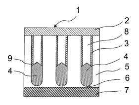
The lighting element 1, 11, 21, 31 as in Fig. 1, 2, 3 and 4 contains a base
electrode 7, 17, 27,
37 of highly reflective aluminium, and arranged on this a porous dielectric
layer 5, 15, 25, 35
of aluminium oxide. The dielectric layer can if required contain a barrier
layer 6, 16, 26, 36 of
a thickness of less than 30 nm, although this is not absolutely necessary. In
the pores 8, 18,
28, 38 there are e.g. galvanically deposited emitter rods 4, 14, 24 made from
metal with
emitter points 9, 19, 29, 39, which are conductively connected to the base
electrode 7, 17,
27, 37. Over the front surface of the dielectric layer 5, 15, 25, 35 there is
a layer of counter-
electrode 2, 12, 22, 32 of indium tin oxide (ITO) deposited e.g. by a vacuum
coating process.
A first version of embodiment (B) is shown in Fig. 1. It is characterised in
that a luminescent
layer 3 is arranged on the free pore inner walls, forming or retaining a
central pore cavity.
The counter-electrode 2 is applied directly to the front surface of the
dielectric layer 5.
A second version of embodiment (B) is shown in Fig. 2. It is characterised in
that part of the
volume of the free pore recess is filled with a luminescent material 13. If
required, the whole
free pore recess 18 can be filled with the luminescent material 13. The
counter-electrode 2
is applied directly to the front surface of the dielectric layer 5.
Fig. 3 shows a first version of the embodiment (A). It is characterised in
that a luminescent
layer 23 covering the pores 28 is applied directly to the front surface of the
dielectric layer 25.
The counter-electrode 22 is applied directly to the luminescent layer 23.
The embodiment in Fig. 4 shows a second version of embodiment (A). It is
characterised in
2o that a perforated layer of intermediate electrode 40 not covering the pore
cavities is directly
applied to the front surface of the dielectric layer 35 and a luminescent
layer 33 covering the
pores 38 is applied directly to the intermediate electrode 40. The counter-
electrode 32 is di-
rectly applied to the luminescent layer 33.
The lighting element in Figs. 1-4 can be used for an operation in accordance
with the princi-
ple (i) of cold-cathode-field emission under direct current conditions, where
electron emis-
sions are generated by application of a voltage. The pore cavities in this
case are either
partly or fully evacuated. The lighting element as in Figs. 1-4 can also be
used in an opera-
tion in accordance with the principle (ii) of gas discharge under alternating
current conditions.
The pores in this case are filled with a plasma-forming gas.