Note: Descriptions are shown in the official language in which they were submitted.
CA 02488832 2004-12-07
WO 2004/001429 PCT/US2003/018882
MULTI-SOCKET BOARD FOR OPEN/SHORT TESTER
FIELD OF INVENTION
This invention relates generally to integrated circuit
testing, and more specifically to an interface structure
for routing test signals between ball grid array packaged
integrated circuits and integrated circuit device testers.
BACKGROUND
Integrated circuit (IC) devices typically include an
IC chip housed in a package formed of plastic, ceramic or
metal. The IC chip includes an integrated circuit formed on
a thin piece (e. g., "chip") of silicon. The package
supports and protects the IC chip and provides electrical
connections between the integrated circuit and an external
circuit or system.
There are several package types, including ball grid
arrays (BGAs), pin grid arrays (PGAs), plastic leaded chip
carriers, and plastic quad flat packs. Each of the package
types is typically available in numerous sizes and
configurations. The package type and configuration selected
by an IC manufacturer for a particular IC chip may be
determined by the size and complexity of the IC chip and/or
in accordance with a customer's requirements.
For example, BGA packages may include any suitable
number of solder balls to provide electrical connections
between the IC chip and an external circuit or system. The
solder balls may be formed over all or a portion of a
bottom surface of the package. For example, BGA packages
that include solder balls formed over the entire package
bottom are said to have a full footprint, while BGA
packages that include solder balls formed around the
periphery of the package bottom are said to have a
peripheral footprint. In addition, the pitch, which may be
defined as the lateral distance between the solder balls,
may vary between BGA packages.
FIGS. 1A and 1B show bottom and side sectional views,
respectively, of a typical BGA package 100 having a full
footprint. BGA package 100 includes a plurality of solder
balls 102 formed on a bottom surface 104a of a substrate
CA 02488832 2004-12-07
WO 2004/001429 PCT/US2003/018882
104. Balls 102 are arranged in a matrix spanning the length
L and width W of substrate bottom surface 104a. An IC chip
106 is mounted on an upper surface 104b of package
substrate 104. Bond wires 108 provide electrical
connections between bonding pads 110 of IC chip 106 and
contact pads 112 formed on substrate 104. Contact pads 112
are electrically connected to corresponding balls 102 by
conductive vias 114 formed in substrate 104. A protective
cover 116, such as a cap or "glob top", is formed over IC
chip 106 and bond wires 108.
FIGS. 2A and 2B show bottom and side sectional views,
respectively, of a typical BGA package 200 having a
peripheral footprint. Like BGA package 100 (FIGS. 1A and
1B), BGA package 200 includes a plurality of solder balls
202 formed on a bottom surface 204a of substrate 204 and
connected to IC chip 206 by bond wires 208 and conductive
vias 214. However, unlike BGA package 100, balls 202 of BGA
package 200 are arranged around the periphery of substrate
bottom surface 204a, thereby leaving a central area of
substrate bottom surface 204a without balls 202.
IC manufacturers typically test their IC packages
before shipping to customers using well-known IC testing
systems. A typical IC testing system includes a device
tester, a device handler, and an interface structure. The
device tester includes a plurality of test probes that
provide test signals to the interface structure, which in
turn transmits signals between the device tester and the
leads (e. g., solder balls) of an IC device under test
(DUT). The device handler is a precise robot that
automatically moves IC devices between a storage area and
the interface structure.
FIG. 3 shows a top view of a conventional interface
structure 300 that may be used to test BGA package 100 of
FIGS. 1A and 1B. Interface structure 300 includes a
rectangular-shaped printed circuit board (PCB) 302 having a
socket 304 located in a central test area. PCB 302 is of a
size and shape that allows it to be received into a docking
area of an associated device tester (not shown). Socket 304
includes a plurality of compressible pins such as pogo pins
306 arranged in a matrix so as to mate with and contact
2
CA 02488832 2004-12-07
WO 2004/001429 PCT/US2003/018882
corresponding balls 102 of BGA package 100 (not shown in
FIG. 3). Thus, the arrangement of pogo pins 306 of socket
304 corresponds to the arrangement of balls 102 of BGA
package 100. PCB 302 includes groups 308 of conductive
contacts 310 positioned around the periphery of socket 304.
Contacts 310 extend through a bottom surface of PCB 302 to
receive corresponding test probes (not shown) extending
from the device tester, and are connected to corresponding
pogo pins 306 of socket 304 by conductive lines (e. g.,
metal traces) 312. For simplicity, only a few conductive
traces 312 are shown in FIG. 3.
The arrangement of contact groups 308 shown in FIG. 3
is compatible with the Model TR-8 MDA tester from Checksum,
Inc. of Arlington, Washington. For simplicity, each group
308 is shown to include 4 contacts 310, although groups 308
may include any suitable number of contacts 310. For
example, for compatibility with the Model TR-8 MDA Tester,
each group 308 includes 48 contacts 310.
FIG. 4 shows an exploded side view of a conventional
IC testing system 350 employing interface structure 300 and
a device tester 352 such as, for example, the Model TR-8
MDA tester. Computer 360, which may be, for example, a
personal computer (PC), is connected to device tester 352
and includes well-known testing software residing in
internal memory (e.g., system memory or a hard disk). BGA
package 100 is mounted on socket 304 (for example, using a
device handler) so that its solder balls 102 contact pogo
pins 306 (not shown in FIG. 4) of socket 304. Interface
structure 300 is mounted on docking area 356 of device
tester 352 so that contacts 310 are aligned with and make
electrical contact with corresponding test probes 354 of
device tester 352. The testing software provides test and
control signals to device tester 352 according to test
parameters associated with BGA package 100. The test
parameters may be stored in a file located in computer
memory, or may be input into computer 360 using any
suitable input device such as, for example, a keyboard (not
shown).
Referring also to FIGS. 1A, 1B, and 3, device tester
352 provides the test signals through test probes 354 to
3
CA 02488832 2004-12-07
WO 2004/001429 PCT/US2003/018882
contacts 310, along traces 312 to socket pogo pins 306, and
finally to corresponding balls 102 of BGA package 100. For
example, a test signal applied to contact 310a by a
corresponding tester probe 354 of device tester 352 is
routed along conductive trace 312a to pogo pin 306a, and
thereafter to a corresponding ball 102 of BGA package 100.
Signals are returned from BGA package 100 to device tester
352 in a similar manner.
A problem associated with conventional interface
structure 300 is that socket 304 can support only one BGA
package size and configuration (e. g., BGA package 100).
Thus, if the physical dimensions of a package substrate do
not match the size of socket 304, or if the number and
placement of its solder balls do not match the arrangement
of pogo pins 306, interface structure 300 cannot be used to
test the package. For example, because BGA package 200 of
FIGS. 2A and 2B has a peripheral footprint rather than a
full footprint, and/or may have a different ball pitch than
BGA package 100 of FIGS. 1A and 1B, interface structure 300
may not be suitable for testing BGA package 200.
Accordingly, an IC manufacturer utilizing several BGA
package sizes and configurations must purchase a separate
interface structure for each BGA package size and
configuration, thereby increasing device testing costs. In
addition, switching between different interface structures
mounted on a device tester undesirably increases testing
time. Thus, there is a need for an interface structure that
allows for testing BGA packages of different sizes and
configurations.
SUMMARY
A method and apparatus are disclosed that allow a
single interface structure to accommodate BGA packages of
different sizes and configurations while preserving
compatibility with an associated device tester. In
accordance with one embodiment of the present invention, an
interface structure includes first and second portions. The
first portion has physical dimensions that are compatible
with the docking area of the associated device tester, and
includes a first socket configured to receive a first BGA
4
CA 02488832 2004-12-07
WO 2004/001429 PCT/US2003/018882
package. The second portion, which is adjacent to and
contiguous with the first portion, extends laterally beyond
the docking area of the device tester to provide additional
testing area that may include one or more additional
sockets. In one embodiment, the second portion includes a
second socket configured to receive a second BGA package,
wherein the second size and configuration of second BGA
package are different from the size and configuration of
the first BGA package. Thus, the first socket has a
plurality of pins for connecting to corresponding solder
balls of the first BGA package, and the second socket has a
plurality of pins for connecting to corresponding solder
balls of the second BGA package. The first portion includes
a plurality of conductive contacts formed in an arrangement
that align with and contact corresponding test probes of
the device tester. Each conductive contact in the first
portion is electrically connected to a corresponding pin in
the first socket by a corresponding first conductive trace,
and electrically connected to a corresponding pin in the
second socket by a corresponding second conductive trace.
Providing an additional test area to include the
second socket advantageously allows first and second BGA
packages having different sizes and/or configurations to be
tested using the same interface board and device tester,
thereby reducing testing costs and saving time. For
example, the interface structure is mounted onto an
associated device tester so that the first portion of the
interface structure aligns with and mates to the docking
area of the device tester, with the second portion
extending beyond the docking area of the device tester.
During a first test procedure, a first BGA package is
mounted on the first socket of the interface structure, and
test signals associated with the first BGA package are
transmitted between the device tester and the first BGA
package to test the first BGA package. The first BGA
package is then removed from the first socket. During a
second test procedure, a second BGA package is mounted on
the second socket of the interface structure. Test signals
associated with the second BGA package are transmitted
between the device tester and the second BGA package to
5
CA 02488832 2004-12-07
WO 2004/001429 PCT/US2003/018882
test the second BGA package.
BRIEF DESCRIPTION OF THE DRAWINGS
The features and advantages of the present invention
are illustrated by way of example and are by no means
intended to limit the scope of the present invention to the
particular embodiments shown, and in which:
FIG. 1A is a bottom view of a conventional BGA package
having a full footprint;
FIG. 1B is a sectional side view of the BGA package of
FIG. 1A taken along line AA;
FIG. 2A is a bottom view of a conventional BGA package
having a peripheral footprint;
FIG. 2B is a sectional side view of the BGA package of
FIG. 2A taken along line AA;
FIG. 3 is a top view of a conventional interface
structure;
FIG. 4 is an exploded side view of a conventional IC
testing system including a device tester and the
conventional interface structure of FIG. 3;
FIG. 5 is a top view of an interface structure in
accordance with one embodiment of the present invention;
FIG. 6 is an exploded side view of an IC testing
system including a device tester and the interface
structure of FIG. 5;
FIG. 7 is a flow chart illustrating one embodiment of
an exemplary test operation of first and second BGA
packages using the interface structure of FIG. 5; and
FIG. 8 is a top view of an interface structure in
accordance with another embodiment of the present
invention.
Like reference numerals refer to corresponding parts
throughout the drawing figures.
DETAILED DESCRIPTION
Embodiments of the present invention are discussed
below in the context of an interface structure that is
compatible with the Model TR-8 MDA tester from Checksum,
Inc. Discussion of this one interface structure is for
simplicity only. It is to be understood that embodiments of
6
CA 02488832 2004-12-07
WO 2004/001429 PCT/US2003/018882
the present invention are equally applicable to interface
structures compatible with other device testers available
from other manufacturers. Further, as used herein, the term
"BGA" refers to any IC product or package having solder
balls for connecting to an external circuit or system. In
addition, the term "package size" is used to describe the
peripheral size and shape of a BGA package substrate, and
the term "configuration" is used to described the spacing
and arrangement of solder balls on a BGA package substrate.
Accordingly, the present invention is not to be construed
as being limited to specific examples described herein but
rather includes within its scope all embodiments defined by
the appended claims.
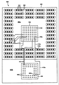
FIG. 5 shows an interface structure 400 in accordance
with one embodiment of the present invention that may be
used to test BGA packages having different package sizes
and/or configurations using the same device tester.
Interface structure 400 includes a printed circuit board
(PCB) 402 having a first portion 402a and a second portion
402b. First portion 402a is similar to conventional
interface structure 300 of FIG. 3, and is of a size and
shape that provides compatibility with the docking area of
an associated device tester. For example, referring also to
FIG. 6, first portion 402a aligns with and mounts onto
docking area 356 of device tester 352 so that contacts 310
included within first portion 402a align with and make
electrical contact with corresponding test probes 354 of
device tester 352. Thus, the first portion 402a includes an
outer peripheral boundary that fits within docking area 356
of device tester 352. For simplicity, each contact group
308 is shown to include 4 contacts 310 to contact
corresponding test probes 354 of device tester 352. For
actual embodiments, contact groups 308 may include any
suitable number of contacts 310 to mate with corresponding
test probes of device tester 352. For one embodiment, each
contact group 308 includes 48 contacts 310 and is
compatible with the Model TR-8 NmA tester from Checksum,
Inc. For other embodiments, contact groups 308 of first
portion 402a of interface structure 400 may be arranged to
align with test probes of other device testers.
7
CA 02488832 2004-12-07
WO 2004/001429 PCT/US2003/018882
First portion 402a includes first socket 304 having a
plurality of first compressible pins such as pogo pins 306
arranged in a matrix so as to mate with and contact
corresponding solder balls of a first BGA package such as,
for example, BGA package 100 of FIGS. lA and 1B. Each pin
306 in first socket 304 is connected to a corresponding
contact 310 formed in first portion 402a by a corresponding
conductive trace 312.
Second portion 402b is adjacent to and contiguous with
first portion 402a, and extends laterally beyond docking
area 356 of device tester 352 to provide additional testing
area, as illustrated in FIG. 6. Thus, second portion 402b
includes an outer peripheral boundary that is entirely
outside docking area 356 of device tester 352. Second
portion 402b includes a second socket 404 having a
plurality of second compressible pins such as pogo pins 406
arranged in a matrix so as to mate with and contact
corresponding solder balls of a second BGA package such as,
for example, BGA package 200 of FIGS. 2A and 2B, where the
size and/or configuration of the second BGA package may be
different from that of the first BGA package. Thus, the
number and arrangement of first socket pins 306 may be
different from the number and arrangement of second socket
pins 406. Each pin 406 in second socket 404 is connected to
a corresponding contact 310 formed in first portion 402a by
a corresponding conductive trace 412. For simplicity, only
a few conductive traces 412 are shown in FIG. 5.
For one embodiment, the second conductive traces 412
formed in second portion 402b extend into first portion
402a and connect to corresponding first traces 312 formed
in first portion 402a. For example, pogo pin 406a of second
socket 404 is connected to second conductive trace 412a,
which in turn is connected to corresponding contact 310a
via first conductive trace 312a. For other embodiments,
second conductive traces 412 may be connected directly to
corresponding contacts 310 in first portion 402a. In this
manner, each contact 310 of interface structure 400 is
connected to a corresponding pin 306 in first socket 304
and to a corresponding pin 406 in second socket 404.
First and second sockets 304 and 404 may be any well-
s
CA 02488832 2004-12-07
WO 2004/001429 PCT/US2003/018882
known IC device test socket. For one embodiment, sockets
304 and 404 are of the type described in commonly owned
U.S. Patent No. 5,955,888. For another embodiment, sockets
304 and 404 are of the type described by Hornchek and Mardi
in commonly owned U.S. Patent No. 6,541,991 entitled
~~Interface Apparatus and Method for Testing Different Sized
Ball Grid Array Integrated Circuits."
As mentioned above, first and second sockets 304 and
404 may be any suitable size and may include any number of
pogo pins positioned in any suitable arrangement to receive
BGA packages of various sizes and configurations. Thus,
although first socket 304 is shown in FIG. 5 as having 64
pins arranged to receive BGA package having a full
footprint, in other embodiments first socket 304 may
include a different number of pins having other
arrangements, for example, to receive a BGA package having
a peripheral footprint. Similarly, although second socket
404 is shown in FIG. 5 as having 48 pins arranged to
receive a BGA package having a peripheral footprint, in
other embodiments second socket 404 may include a different
number of pins having other arrangements, for example, to
receive a BGA package having a full footprint. Further, the
respective pin pitches of first socket 304 and second
socket 404 may vary as desired to provide compatibility
with different BGA packages to be tested.
For one embodiment, first socket 304 includes a full
matrix of 2048 pins 306 having a pitch of 1 mm to receive a
compatible 45mm x 45mm BGA package, and second socket 404
includes a peripheral matrix of 560 pins 406 having a 1.27
mm pitch to receive a compatible 42.5mm x 42.5mm BGA
package. For another embodiment, second socket 404 includes
a peripheral matrix of 352 pins 406 having a 1.27 mm pitch
to receive a compatible 35mm x 35mm BGA package.
Referring to the flow chart of FIG. 7, interface
structure 400 is prepared for testing various BGA packages
as follows, with reference also being made to FIGS. lA, 1B,
2A, 2B, 5, and 6. Interface structure 400 is mounted onto
device tester 352 so that first portion 402a is aligned
over docking area 356 and test probes 354 are connected to
corresponding contacts 310 of first portion 402a, as shown
9
CA 02488832 2004-12-07
WO 2004/001429 PCT/US2003/018882
in FIG. 6 (step 700). A device handler (not shown)
positions a first BGA package (e. g., BGA package 100) into
first socket 304 of interface structure 400 so that pogo
pins 306 of first socket 304 contact corresponding solder
balls of the first BGA package (step 702). Well-known
testing software executing on computer 360 loads testing
parameters associated with the first BGA package, and
transmits appropriate test and control signals to device
tester 352 in a well-known manner (step 704). Device tester
352 then transmits test signals to and from the first BGA
package (step 706). For example, test signals provided by
device tester 352 are provided to contacts 310 in first
portion 402a via corresponding test probes 354 and
thereafter transmitted to corresponding solder balls of the
first BGA package via conductive traces 312 and first
socket pogo pins 306. Upon completion of the test signal
transmission, the device handler removes the first BGA
package from first socket 304 (step 708).
Then, the device handler positions the second BGA
package (e.g., BGA package 200) into second socket 404 of
interface structure 400 so that pogo pins 406 of second
socket 404 contact corresponding solder balls of the second
BGA package (step 710). The testing software executing on
computer 360 loads testing parameters associated with the
second BGA package, and transmits appropriate test and
control signals to device tester 352 in a well-known manner
(step 712). Device tester 352 then transmits test signals
to and from the second BGA package (step 714). For example,
test signals provided by device tester 352 are provided to
contacts 310 in first portion 402a via corresponding test
probes 354 and thereafter transmitted to corresponding
solder balls of the second BGA package via conductive
traces 312 and 412 and second socket pogo pins 406. Upon
completion of the test signal transmission, the device
handler removes the second BGA package from second socket
404 (step 716).
Because contacts 310 of interface structure 400 are
connected to both first socket pins 306 via first
conductive traces 312 and to second socket pins 406 via
second conductive traces 412, test signals provided to
CA 02488832 2004-12-07
WO 2004/001429 PCT/US2003/018882
interface structure 400 by device tester 352 are
automatically routed to both sockets 304 and 404, thereby
eliminating the need for any switching circuitry between
contacts 310 and sockets 304 and 404. Accordingly, only one
of sockets 304 and 404 should receive a corresponding BGA
package for testing at any given time. For other
embodiments, interface structure 400 may include switching
circuitry to selectively route test signals from contacts
310 to either first socket 304 or second socket 404.
Interface structures in accordance with the present
invention may include more than one test socket in the
additional test area provided by second portion 402b. For
example, FIG.~8 shows an interface structure 500 that
includes a first portion 502a having a first socket 304,
and a second portion 502b having a second socket 504 and a
third socket 508. First socket 304 includes a plurality of
first compressible pins such as pogo pins 306 arranged in a
matrix so as to mate with and contact corresponding solder
balls of a first BGA package such as, for example, BGA
package 100, as described above with respect to FIG. 5.
Second socket 504 includes a plurality of second
compressible pins such as pogo pins 506 arranged in a
matrix so as to mate with and contact corresponding solder
balls of a second BGA package (not shown) having a size
and/or configuration different from that of the first BGA
package (not shown). Each pin 506 in second socket 504 is
connected to a corresponding contact 310 formed in first
portion 502a by a corresponding second conductive trace
512. For example, pin 506a of second socket 504 is
connected to contact 310a by second conductive trace 512a
and first conductive trace 312a. For simplicity, only a few
conductive traces 512 are shown in FIG. 8.
Third socket 508 includes a plurality of third
compressible pins such as pogo pins 510 arranged in a
matrix so as to mate with and contact corresponding solder
balls of a third BGA package (not shown) having a size
and/or configuration different than that of the first and
second BGA packages (not shown). Each pin 510 in third
socket 508 is connected to a corresponding contact 310
formed in first portion 502a by a corresponding conductive
11
CA 02488832 2004-12-07
WO 2004/001429 PCT/US2003/018882
trace 512.
For one embodiment, the second, conductive traces 512
formed in second portion 502b extend into first portion
502a and connect to corresponding first traces 312 formed
in first portion 502a. For example, pogo pin 506a of second
socket 504 and pogo pin 510a of third socket 508 are
connected to second conductive trace 512a, which in turn is
connected to corresponding contact 310a via first
conductive trace 312a. For other embodiments, second
conductive traces 512 may be connected directly to
corresponding contacts 310 in first portion 502a. In this
manner, each contact 310 of interface structure 500 is
connected to a corresponding pin 306 in first socket 304,
to a corresponding pin 506 in second socket 504, and to a
corresponding pin 510 in third socket 508.
In yet another embodiment, more than one additional
test area such as 502b is provided, and thus accommodates
more different types of sockets to allow testing of more
types of devices without removing an interface structure.
Sockets 304, 504, and 508 of interface structure 500
may be any suitable size and may include any number of pogo
pins positioned in any suitable arrangement to receive BGA
packages of various sizes and configurations. For one
embodiment, first socket 304 includes a full matrix of 2048
pins 306 having a pitch of 1 mm to receive a compatible
45mm x 45mm BGA package, second socket 504 includes a
peripheral matrix of 560 pins 406 having a 1.27 mm pitch to
receive a compatible 42.5mm x 42.5mm BGA package, and third
socket 508 includes a peripheral matrix of 352 pins 406
having a 1.27 mm pitch to receive a compatible 35mm x 35mm
BGA package.
12