Note: Descriptions are shown in the official language in which they were submitted.
CA 02489237 2004-12-10
WO 2003/107441 PCT/US2003/019000
1
P0254US-7 PATENT
SATURATED PHOSPHOR SOLID STATE EMITTER
This application claims the benefit of provisional
application Serial Number 60/388,327 to Keller et al.,
which was filed on June 13, 2002.
BACKGROUND OF THE INVENTTON
Field of the Invention
This invention relates to solid state emitters and
more particularly to light emitting diodes (LEDs) laser
diodes whose wavelength of emitted light is converted by a
1S conversion material.
Description of the Related Art
Light emitting diodes (LEDs) are solid-state devices
that convert electric energy to light, and generally
comprise an active layer of semiconductor material
sandwiched betweeri, two oppositely doped semiconductor
layers. When a bias is applied across the doped layers,
holes and electrons are injected into the active layer
where they recombine to generate light. Light is emitted
omnidirectionally from the active layer and from all
surfaces of the LED. Recent advances in LEDs (such as Group
III nitride based LEDs) have resulted in highly efficient
light sources that surpass the efficiency of filament-based
z
light sources, providing light with equal or greater
brightness in relation to input power.
Solid-state semiconductor laser diodes convert
electrical energy to light in much the same way as LEDs.
CA 02489237 2004-12-10
WO 2003/107441 PCT/US2003/019000
2
They are structurally similar to LEDs but include mirrors
on two opposing surfaces', one of which is partially
transmissive. In the case of edge emitting lasers, the
mirrors are on the side surfaces; the mirrors provide
optical feedback so that stimulated emission can occur.
This stimulated emission provides a highly
collimated/coherent light source. A vertical cavity laser
works much the same as an edge emitting laser but the
mirrors are on the top and the bottom. It provides a
l0 similar collimated output from its trip surface. Some types
of solid-state lasers can be, more efficient than LEDs at
converting electrical current to' light.
Green emitting LEDs can be fabricated from different
material systems including the Group III nitride based
material system. Conventional green emitting LEDs, however,
are typically subject to low yield and are considered
difficult to fabricate with uniform emission
characteristics from batch to batch. The LEDs can also
exhibit large wavelength variations across the wafer within
a single batch, and can exhibit strong wavelength and
emission variations~with operation conditions such as drive
current and temperature.
Phosphors, polymers and dyes have been used to
surround LEDs to downconvert the LED's light to a different
wavelength., thereby modifying the light emitted by the LED.
For example, a single blue emitting LED has been surrounded
with a yellow phosphor, polymer or dye, with a typical
phosphor being cerium-doped yttrium aluminum garnet
(Ce:YAG). [See Nichia Corp. white LED, Part No. NSPW300BS,
NSPW312BS, etc.; See also U.S. Patent No. 5,959,316 to
Lowery, "Multiple Encapsulation of Phosphor-LED Devices"].
The surrounding phosphor material "downconverts" the
wavelength of some of the LED light and re-emits it as a
CA 02489237 2004-12-10
WO 2003/107441 PCT/US2003/019000
3
different wavelength such that the overall "LED package"
emits two wavelengths of light. In the case of a blue
emitting LED surrounded by a yellow phosphor, some of the
blue light passes through the phosphor without being
converted, while the remaining light is downconverted to
yellow. The blue light passing through the phosphor plays a
major role in the overall color of light emitted by the LED
package, which emits both blue and yellow light that
combine to provide a white light.
l0 In these types of LED packages, it can be difficult to
apply the downconverting material in such a way that the
light source (LED) emits homogeneous light. Replicability
and mass production also presents problems because even
slight fluctuations in the layer thickness of the
conversion material can change the color of emitted light.
U.S. Patent No. 6,066,861 to Hohn et al. discloses a
Basting composition that surrounds an LED and contains
conversion material in stable dispersion such that the
light from the LED appears more homogeneous. In one
embodiment, the conversion material (luminous substance): is
a phosphor group Q~f the general formula A3B5X12:M having
particles sizes <20 ~m and a mean grain diameter d5o<5 ~.m.
Similar to the LED package having a yellow conversion
material surrounding a blue LED, the casting composition is
~S arranged so that a substantial portion of the LED light
passes through, while the remaining LED light is
downconverted.
Another disadvantage of the typical blue LED
surrounded by a yellow downconverting material is that the
resulting white light can have an unacceptable color
temperature and poor color rendering such that the LED is
not suitable for standard room lighting. U.S. Patent No.
6,252,254 to Soules et a1. discloses a blue LED (or a laser
CA 02489237 2004-12-10
WO 2003/107441 PCT/US2003/019000
4
diode) covered with a green and red downconverting
phosphor. Similar the blue LED surrounded by yellow
downconverting material, the green/red phosphor absorbs
some of the blue LED light and reemits red and green light,
such that the LED and phosphor both emit light that
combines as a white light. Soules et al. discloses that the
resulting white light has an improved color temperature and
improved color rendering.
Another disadvantage of a typical blue LED with yellow
downconverting material is that the material can
deteriorate, leading to color tone deviation and darkening
of the fluorescent material. U.S. Patent No. 5,998,925 to
Shimuzu et al. discloses a LED to address this
disadvantage by providing a light emitting component (e. g.
Z5 LED or laser diode) and a phosphor capable of absorbing
part of the light emitted by the light emitting component
and emitting light of a wavelength different from that of
the absorbed. light. The light emitting component comprises
a nitride based semiconductor and the phosphor contains a
particular garnet fluorescent material. Shimuzu et al.
discloses that th~~ phosphor has excellent resistance to
light so that the fluorescent properties experience little
deterioration when used over an extended period of time.
Light extraction is another recognised problem with
conventional LEDs, which typically have an active layer and
doped layers with a refractive index n of about 3.5. The
LEDs are then encapsulated in an epoxy having a refractive
index n of about 1.5. Application of Snell's law shows that
only light emitted from the active region within an angle
theta of. about 0.443 radians to normal of the interface
with the epoxy can exit from the top of the LED. For larger
angles, the light is trapped within the LED by total
internal reflection, such that only a fraction of the Light
CA 02489237 2004-12-10
WO 2003/107441 PCT/US2003/019000
(approximately 9.6% in some cases) contributes to light
emission. U.S. Patent No. 5,813,753 to Vriens et al.
discloses a UV/blue LED phosphor device with enhanced
conversion and extraction of Light. The device utilizes
5 most of the LED's edge emitted light by the appropriate
positioning of reflectors and phosphor. The device also
affects angular emission and color of the visible light
emitted by the UV/blue LED-phosphor device by the use. of
one or more dielectric filters on the device. In one
embodiment, a light emitting device is placed in a cup-
shaped header with a reflector that is then filled with a
transparent material having a homogeneously mixed phosphor.
The device anticipates that not all of the light will be
absorbed by the phosphor and includes a glass plate that is
l5 placed on the device that prevents UV/blue light which is
not absorbed by the phosphor grains from exiting into air.
In another embodiment a long wave pass filter (LPW) is
added adjacent to the glass plate to reflect UV/blue light
back to the phosphor and to transmit visible light emitted
by the phosphor
All of the LEl~~packages described above have a common
characteristic. Each relies on or contemplates that a
portion of the light from the LED (or laser diode) passes
through the conversion material without being absorbed and
in most cases the light passing through plays an important
role in the overall color emitted by the package.
SUMMARY OF THE INVENTION
The present~invention seeks to provide solid state
emitter packages that are easy to manufacture and provide a
high yield, while at the same time providing emitter
packages exhibiting limited wavelength variations between
batches of packages and exhibit consistent wavelength and
CA 02489237 2004-12-10
WO 2003/107441 PCT/US2003/019000
6
emission characteristics with operation over time. One
embodiment of a saturated conversion material emitter
package according to the present invention comprises a
semiconductor emitter and a conversion material. The
conversion material is arranged to absorb substantially all
of the light emitting from the semiconductor emitter and
re-emit light at one or more different wavelength spectrums
of light. The conversion material is also arranged so that
there is not an excess of conversion material to block the
re-emitted light as it emits from the emitter package. The
emitter package emits light at the one or more wavelength.
spectrums from the conversion material.
Another embodiment of a saturated conversion material
emitter package according to the present invention
comprises one or more semiconductor emitters, each of which
emits light in response to a bias. A metal cup is included
with the semiconductor emitters arranged at the base of the
cup. A plurality of conductive paths are coupled to the
semiconductor emitters for applying a bias to the emitters
to cause them to emit light. A conversion material is
arranged so that light from the emitters passes through the
conversion material, with the conversion material absorbing
substantially all light from the emitters and re-emitting
light at one or more different wavelengths of light . The
conversion material is also arranged so that it does not
substantially block the re-emitted light as it emits from
the emitter package. The emitter package emits light at the
one or more wavelength spectrums from the conversion
material.
In~one embodiment of an emitter package according to
the present invention, the semiconductor emitter comprises
a blue of UV emitting LED, with the LED light passing
through a green phosphor. The phosphor is saturated.by the
CA 02489237 2004-12-10
WO 2003/107441 PCT/US2003/019000
7
light such that the package emits in the green portion of
the spectrum. This arrangement offers a number of
advantages over convention nitride-based green LEDs. Unlike
green LEDs, the emission spectrum of green phosphor is
essentially fixed by the specific material and is
accordingly less subject to wavelength variation. Phosphors
in general can also have a spectrally broader emission
spectrum, which may be desirable in some applications.
The light from an LED passing through a saturated
conversion material according to the present invention can
be subject to losses due to non-unity conversion efficiency
of the phosphor and the Stokes shift. This loss, however,
is acceptable because the preferred embodiments of LED
packages according to the present invention comprise high
efficiency, high yield LEDs, such as UV and blue emitting
Group III nitride-based LEDs, which compensate for the
losses and result in a LED package with higher emission
efficiency compared to typical LEDs.
This technology is well suited for manufacturing and
the development of a wide variety of flexible products for
solid-state lighting. The possible applications of LED
packages according to the present invention include, but
are not limited to, traffic lights, displays, specialty
illumination, signals, etc. The invention also can be used
in combination with blue and red emitters to fabricate a
v
white light emitting LED package, which would be suited for
nearly any application requiring high efficiency, high
color rendering solid-state lighting. This includes indoor
and outdoor commercial and residential architectural
lighting, auto taillights,,displays, flashbulbs and general
lighting. This will result in cumulative energy saving and
reduction of environmental impacts.
These and other further features and advantages of
CA 02489237 2004-12-10
WO 2003/107441 PCT/US2003/019000
8
the invention will be apparent to those skilled in the art
from. the following detailed description, taken together
with the accompanying drawings, in which:
BRIEF DESCRIPTION OF 'THE DRAWINGS
FIG. 1 is a sectional view of one embodiment of a
saturated conversion material LED package according to the
present invention;
FIG. 2 is a graph showing the output intensity verses
l0 peak emission wavelength of a saturated conversion material
LED according to the present invention;
FIG. 3 is a graph showing the wavelength spectrum of
saturated conversion material LED according to the present
invention;
FIG. 4 is a graph showing the output loss verses
operating hours for saturated conversion material LEDs
according to the present invention.
FIG. 5 is a sectional view of another embodiment of a
saturated conversion material LED package according to the
present invention;
FIG. 6 is a sectional view of one embodiment of a
c
saturated conversion material semiconductor laser package
according to the present invention;
FIG. 7 is a sectional view of an embodiment of a
saturated conversion material emitter package according to
the present invention having different concentration layers
of conversion material; and
FIG. 8 is a sectional view of an embodiment of a
saturated conversion material emitter package according to
the present invention having homogeneous concentration of
conversion material.
CA 02489237 2004-12-10
WO 2003/107441 PCT/US2003/019000
9
DETAILED DESCRIPTION OF THE INVENTION
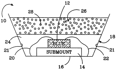
FIG. 1 shows one embodiment of a saturated conversion
material LED package 10 according to the present invention.
It comprises an LED'12 (although more than one LED can be
used) which generally includes an active layer sandwiched
between two oppositely doped layers. The layers have
standard thicknesses and the active layer emits light
omnidirectionally when a bias is applied across the
oppositely doped layers. The layers of the LED 12 can be
made of many different semiconductor material systems and
the LED 12 can emit many different colors of light. The LED
12 preferably emits blue light and can be formed of a
semiconductor material from the Group III nitride based
material system, which provides for high efficiency
radiation of blue light. Group III nitrides refer to those
semiconductor compounds formed between nitrogen and the
elements in Group III of the periodic table, usually
aluminum (Al), gallium (Ga), and indium (In). The term
also refers to ternary and tertiary compounds such as AlGaN
and AlInGaN.
The LED 12 c~n also comprise a substrate with the
LED's active and oppositely doped layers formed in a stack
~on the substrate. The substrate can be formed of many
different materials such as sapphire (A12O3) , silicon (Si)
or silicon carbide (SiC), with the preferred substrate
being a 4H polytype of SiC. Other SiC polytypes can also be
used including 3C, 6H and 15R polytypes. A buffer layer can
also be included between the substrate and other LED layers
to provide an appropriate crystal structure transition.
Silicon .carbide has a much closer crystal lattice match to
Group III nitrides than sapphire and results in Group III
nitride films of higher quality. Silicon carbide also has a
very high thermal conductivity so that the total output
CA 02489237 2004-12-10
WO 2003/107441 PCT/US2003/019000
power of Group III nitride devices on silicon carbide is
not limited by the thermal dissipation of the substrate (as
is the case with some devices formed on sapphire). The
availability of silicon carbide substrates also provides
5 the capacity for device isolation and reduced parasitic
capacitance that make commercial devices possible. SiC
substrates are available from Cree Research; Inc., of
Durham, North Carolina and methods for producing them are
set forth in the scientific literature as well as in a U.S.
10 Pat. Nos. Re. 34,861; 4,946,547; and 5,200,022.
The LED's active layer and oppositely doped layers are
formed on the substrate using known semiconductor
fabrication processes, such as metal-organic chemical vapor
deposition (MOCVD). Similarly, techniques for epitaxial
growth of Group III nitrides have been reported in
scientific literature, and in U.S. Pat. Nos. 5,210,051;
5,393,993; 5,523,589; and 5,292,501.
The LED 12 can also comprise first and second
contacts, each of which are arranged in ohmic contact with
a respective oppositely doped layer. A bias applied to the
contacts is condutcted to the oppositely doped layers,
r
resulting in electrons and holes being injected into the
LED's active region where they recombine to cause the
active layer to emit light.
The LED 12 can also be mounted on a submount 14 for
mechanical stability. The submount 14 can contain
electrical circuitry for controlling the amount of current
or power applied to the LED 12 or to otherwise modify the
electric signal applied to the LED 12. The submount 14 can
also contain components and circuitry. to make the LED
package 10 resistant to electrostatic shock. The submount
14 is mounted at the horizontal base 16 of "metal cup" 18
that typically has first and second conductive paths 20, 22
CA 02489237 2004-12-10
WO 2003/107441 PCT/US2003/019000
Z1
for applying a bias across the LED's contacts to cause the
LED 12 to emit light. Alternatively, the bias can be
applied to the LED (or its contacts) fully or partially
through the submount 26 and its electronic circuitry. The
cup 18 can have a reflective surface 20 that reflects light
emitted from the LED 12 so that it contributes to the
overall light emitted from the package l0.
The LED 12, submount 14 and conductive paths 20, 22
are encased in a protective layer 24 that is made of a
radiation hard and transparent material such as a silicon,
resin, or epoxy, with the preferred material being an
epoxy. During manufacturing of the package ZO the epoxy is
injected into and fills the bottom portion of the cup 18
such that the LED 12, the submount 16, and conductive paths
20, 22 are covered by the epoxy, and the epoxy is then
cured.
The LED Z2 further comprises a conversion material
layer 26 on top of the transparent material 24 , with . the
layer 26 also being made of a radiation hard and
transparent material similar to layer 24, and also has a
conversion material!~28 distributed throughout. The material
28 can be one or more fluorescent or phosphorescent
material such as a phosphor, fluorescent dye or
photoluminescent semiconductor. The following list
phosphors that can be used as the conversion material 28,
grouped by the re-emitted color following excitation:
RED
YZO2S : Eu3+, Bi3+
YV04 : Eu3~, Bi3+
SrS : Euz+
SrY2S4 : Eua+
CaLa254:Ce3+
(Ca, Sr) S : Euz+
CA 02489237 2004-12-10
WO 2003/107441 PCT/US2003/019000
12
Y2O3 : Eu3+, Bi3+
Lu2Oz : Eu3+
(Srz_xLax) (Cel-xEux) 04
Sr2Ce1_XEuX04
Sr2_XEuxCe04
Sr2Ce04
SrTi03 : Pr3+, Ga3+
ORANGE
SrSiO3 : Eu, Bi
YELLOW/GREEN
YB03 : Ce3+, Tb3+
BaMgAllo017 : Eu2+, Mn2+
(Sr, Ca, Ba) (Al, Ga) 2S4 : Eu2+
ZnS : Cu+, A13+
LaPO4 : Ce , Tb
CaBMg ( Si04 ) 4C12 : Eu2+, Mn2+
(. (Gd, Y, Lu, Se, La, Sm) 3 (Al, Ga, In) 5012 : Ce3+
( (Gd, Y) 1_xSmx) s (All-yGay) sOlz : Ce3+
(Y1_p_q_rGdpCeqSmr) 3 (All_yGay) sOlz
Y3 (All_SGas) s012 : Ce3+
(Y, Ga, La) 3A1s012 : Ce3+
Gd3Ins012 : Ce3+
(Gd, Y) 3A1s012 : Ce3+, pr3+
Ba2 (Mg, Zn) Si2O7: Eu2+
(Y, Ca,Sr)3(Al,Ga,Si)s(O,S)12
Gdo,46sr0.31A11.23~xF1.38:Eu2+0.06
(Bal _x_ySrxCay) SiO4 : Eau.
Ba2S i04 : Eu2+ r
BLUE
ZnS:Ag,Al
COMBINED YELLOW/RED
Y3A1s012 : Ce3+, pr3+
WHITE
SrS : Eu2+; Ce3+., K+
From the list above, the following phosphors are most
suitable for use as the conversion material 28 in LED
CA 02489237 2004-12-10
WO 2003/107441 PCT/US2003/019000
13
package 10 by having excitation in the blue and/or UV
emission spectrum, providing a desirable peak emission,
having efficient light conversion, and acceptable Stokes
shift
RED
Lu203 ; Eu3+ . ,
(Sr2_xLax) (Cel_xEux) 04
Sr2Ce1 _xEux04
Sr2_xEuxCe04
SrTi03 : Pr3+, Ga3+
YELLOW/GREEN
( Sr, Ca , Ba ) (AI , Ga ) 254 : Eu2+
Ba2(Mg,Zn)Si207:Eu2*
2+
Gd0.46Sr0.31A11.23~xF1.38 : Eu o.06
( Baz_x_ySrxCaY) S i04.: Eu
Ba2Si04 : Eu2+
During manufacturing, the conversion material layer 26
is injected on top of the layer 24 to fill most, or all, of
the cup 18, and is cured. The particles in material 28
absorb light emitted by the UV LED 12 and re-emit the
absorbed light at cane or more wavelength spectrums that are
different from the absorbed wavelength. The conversion
material 28 can comprise more than one type of material,
each of which re-emits light at a different wavelength so
that the conversion material layer 26 re-emits more than
one wavelength of light. The conversion material 28 can
also be in different concentrations throughout the
conversion material layer 26.
The amount of LED light absorbed and re-emitted by the
conversion material is generally proportional to the amount
of conversion material that the LED light passes through.
However, if the LED light passes through too much
conversion material 28, part of the conversion material's
CA 02489237 2004-12-10
WO 2003/107441 PCT/US2003/019000
14
re-emitted light can be blocked from emitting from the LED
package lOr by excess conversion material 28. This can
reduce the overall light emitting efficiency of the package
10. The amount of conversion material that the LED light
passes through can be varied by varying the concentration
of conversion material 28 or varying the thickness of the
layer 26, or both.
In LED package 10, light from the LED 12 passes
through a sufficient amount of conversion material 28 so
that substantially all of the LED light is absorbed and re
emitted at a different wavelength of light. At the same
time, the re-emitted light does not pass through an excess
conversion material 28 so that the re-emitted light is not
blocked from emitting from the package 10. By providing a
sufficient amount of conversion material 28 to provide full
conversion without blocking, the conversion material 28 is
in a "saturation" condition. The amount of conversion
material for conversion material saturation depends on the
size and luminous flux of the LED 12(or laser). The greater
the size and luminous flux, the greater the amount of
conversion materia2 28 needed.
In conversion material saturation, the emitted light
from the package 10 is composed primarily of photons
produced by the conversion material 28. However, in some
embodiments it may be desirable to allow a small portion of
the LED light to be transmitted through the conversion
material 28 without absorption for the purpose of modifying
slightly the chromaticity of the resulting package
radiation. For the LED 10, most embodiments of the package
10 emit.. less than 10% of the emission power of primary
radiation in the absence of the conversion material 28;
i.e. the conversion material 28 absorbs 900 or more of the
light from the LED 12.
CA 02489237 2004-12-10
WO 2003/107441 PCT/US2003/019000
As described above, the LED 12 is blue emitting and a
suitable conversion material is a green phosphor such as
SrGa2S4:Eu2+ (Sr:Thiogallate) or Gdo_46Sro,31A11.23GxF1.ae:Eu+ao.os.
Sr:Thiogallate has a peak excitation wavelength ranging
5 from 400 to 450nm anal the percent of blue light (or Uv
light) that is absorbed by Sr:Thiogallate and then re-
emitted as green light is estimated to be 74% '-~/-So, which
makes this phosphor one of the more efficient for
excitation in the blue (or ITV) range. The use of a high
10 efficiency blue emitter in combination with a phosphor that
is efficient for excitation in the blue range, results in a
saturation conversion material LED package that efficiently
emits green.
FTGs. 2-4 show results of performance studies
15 completed by applicants on LED packages IO according to the
present invention having a blue LED with green conversion
.material in, or near, saturation. FIG. 2 shows a graph 40
plotting the emission performance in Lumens of four
different LED packages according to the present invention
at their peak emission wavelength in nanometers (nm), with
35omA applied across the LED in each package. Using a green
Sr:Thiogallate phosphor as the conversion material, the LED
package emitted up to 58 Lumens at its peak wavelength of
approximately 530nm, which is a significant improvement
over the performance of typical green emitting LEDs.
FIG. 3 shows a graph 50 plotting the emission spectrum
as Tntensity in a.u. verses wavelength in nm, of the light
re-emitted from green Sr:Thiogallate phosphor from the LED
packages. Each package exhibited a similar spectrum having
a peak (~~70rim full width at half maximum (FWHM) centered at
-.530-550nm, which is close to the peak of the general
photopic human eye response curve. This results in an
emission of green light having high efficacy. Applicants
CA 02489237 2004-12-10
WO 2003/107441 PCT/US2003/019000
16
also maintained the operation of each of the LED packages
under test and each maintained this emission spectrum
without change for approximately 168 hours, showing that
the LED packages are stable over time.
FIG. 4 shows a graph 60 that plots the light output
loss over operating hours for three of the four LED
packages 10 under test. The graph 60 illustrates that for
each, the light output loss is minimal over time. This also
shows that the LED packages 10 are stable over time and
this performance is consistent with the performance of
standard green emitting LEDs.
FIG. 5 shows another embodiment of an LED,package 70
according to the present invention, having many similar
features as the.package 10 in FIG. 1. It comprises an LED
72 mounted to a submount 74, which is then mounted to the
horizontal base 76. of a metal cup 78. First and second
conductors 80, 82 are provided to apply a bias across the
LED 72, although a bias can be applied in other ways as
described above. A protective layer 84 is included over
the LED 72, submount 74 and conductive paths 80, 82, and a
conversion materiel layer 86 is included on top of the
protective layer 84 and includes a conversion material 88.
The LED 72 is UV emitting and can be made of many
different material systems, with a preferred material
system being the Group III nitride material system. The
conversion material 88 can be any of the materials listed
above, but is preferably a green phosphor such as
. Sr:Thiogallate. The thickness of layer 86 and the
concentration of Sr:Thiogallate is such that the conversion
material.88~is in saturation, i.e. all of the UV light is
absorbed without an excess of conversion material 88
blocking emission of the re-emitted green light.
Sr:Thiogallate is efficient at absorbing W light~and re
CA 02489237 2004-12-10
WO 2003/107441 PCT/US2003/019000
17
emitting green light, and using this phosphor in
combination with a high efficiency UV LED 72 results in a
saturated conversion material LED package 70 that
efficiently emits green light.
FIG. 6 shows an embodiment of laser diode package 90
according to the present invention having similar features
to the packages 20, 70 described above, but'~instead of
having a LED as a light source, the package 90 has a solid-
state semiconductor laser diode 92. Mirrors 94, 96 are
included on two opposing surfaces of the laser diode 92,
with mirror 94 being partially transmissive. The mirrors
~94, 96 provide optical feedback ~so that stimulated emission
can occur, which provides a highly collimated/coherent
light source. The laser diode 92 can be mounted to a
submount 98 that is then mounted to the horizontal base 100
of a metal cup 102 having conductors paths 104, 106 to
apply a bias to the laser diode 92. The laser diode 92,
submount 98 and conductive paths 104, 106 are covered in a
protective layer 108. A conversion layer 110.is included on
the protective layer 108 and comprises a conversion
material 112, whicl~~can be any of the conversion materials
discussed above.
Different laser diodes emitting different colors of
light can be used for diode 92 and the conversion material
112 is arranged so that the light from the laser diode 92
passes through it and the LED package 90 operates in
saturation of the conversion material 122. All (or most) of
the light from diode 92 is absorbed by the conversion
material, 112 and re-emitted as a different wavelength of
light, while minimizing the amount of re-emitted light
blocked by eaccess conversion material 112.
To improve the uniformity of light emitting from the
package 90, it can be desirable to scatter the light as it
CA 02489237 2004-12-10
WO 2003/107441 PCT/US2003/019000
18
' passes through the layers 108, 110, particularly in the
case of collimated/coherent light from the laser diode 92.
One way to. scatter light is by using scattering particles
114 that randomly refract light. To effectively scatter
light, the diameter of the particles 114 should be
approximately one half of the wavelength of the light being
scattered. In package 90 the scattering parti.'cles 114 are
shown in layer 110, although they can also be included in
layer 108 or formed in another layer arranged on the layer
ZO 110. Light from the diode 92 passes through the particles.
114 and is refracted to mix and spread the light as it
passes through the conversion material.
The scattering particles , 114 are shown evenly
distributed throughout layer 100 but they can also be
distributed in varying concentrations throughout the layer
114 to most effectively scatter the light by matching the
pattern of LED light passing through the layer 114. The
preferred, scattering particles .would not substantially
absorb laser diode light and would have a substantially
different index of refraction than the material in which it
is embedded (for example, epoxy). The scattering particles
114 should have as high of an index of refraction as
possible. Suitable scattering particles can be made of
titanium oxide (Ti02) which has a high index of refraction
(n=2.6 to 2.9) and is effective at scattering. light. Since
the primary requirement for the scattering "particles" is
that they have a different index of refraction from their
surrounding material and that they have a particular size
range, other. elements such as small voids or pores could
also be.used as "scattering particles". .
FIG. 7 shows another embodiment of an emitter package
120 having a semiconductor emitter 122 that is either a LED
or a laser diode. Like the packages 10, 70 .and 90 above,
CA 02489237 2004-12-10
WO 2003/107441 PCT/US2003/019000
19
the package 120 has a submount 124, reflective cup 126,
first and second conductors 128, 130, a protective layer
132 and a conversion material layer 134. However, in the
package 120 the protective layer 232 contains a
concentration of conversion particles 136 that is different
from the concentration of conversion particles 138 in layer
134. The particles 136 can also be a different type from
the particles 138, such that layer 132, 134 each re-emits a
different color of light. Tn both embodiments, the package
120 is arranged to operate in conversion material
saturation.
FIG. 8 shows another embodiment of an emitter package
150 according to the .invention that is the same as the
package 120 in FIG. 4, but instead of having a protective
Layer 132 and a conversion material layer 134 as shown in
FIG. 4, the cup 152 in package 150 is filled with a single
conversion layer 156 that serves to protect the packages
emitter 158, submount 160, and conductive paths 162, 164
and contains a the conversion material 166 distributed
throughout. The conversion material can be homogeneously
distributed or distributed in different concentrations.
Like above, the package 150 operates in conversion material
saturation such that all (or most) of the light from the
emitter 158 is absorbed and re-emitted without the
conversion material 166 significantly blocking the re-
emitted light.
Although the present invention has been described in
considerable detail with reference to certain preferred
configurations thereof, other versions are possible, Each
of the .LED package embodiments described above can have
different components having different features. Each of the
LED packages above can have emitters made of different
material systems and each can include scattering particles.
CA 02489237 2004-12-10
WO 2003/107441 PCT/US2003/019000
Other conversion materials beyond those listed above can be
used. Therefore, the spirit and scope of the invention
should not be limited to the preferred versions of the
invention described above.