Note: Descriptions are shown in the official language in which they were submitted.
CA 02489345 2004-12-09
WO 03/107522 PCT/US03/18338
IMPEDANCE SOURCE POWER CONVERTER
BACKGROUND OF THE INVENTION
[0001] The present invention is directed to a power converter and, more
specifically, an
impedance source power converter.
[0002] Power converters are utilized in various applications and have
traditionally been
constructed as either voltage source converters (V-converters) or current
source
converters (I-converters). In a typical V-converter, a DC voltage source feeds
a main
converter circuit, for example, a three-phase bridge. The DC voltage source
may take
various forms, such as a battery, a fuel cell stack, a diode rectifier and/or
a capacitor.
In a typical three-phase bridge, six switches are utilized to implement the
main converter
circuit. Fig. 1 depicts a traditional three-phase V-converter 100, which
includes six
switches S1-S6, which may each include a power transistor and an anti-parallel
(i.e.,
free wheeling) diode to provide bi-directional current flow and uni-
directional voltage
blocking, that are fed by a DC voltage source 102. The switches S1-S6 are
controlled
by a control unit (e.g., a programmed microcontroller) 106 to provide a
desired output.
[0003] The V-converter has a number of conceptual and theoretical limitations.
For
example, an AC output voltage of a V-converter is limited below and cannot
exceed a
voltage level of an associated DC voltage source or the level of the DC
voltage source is
greater than an AC input voltage. As such, the V-converter is a buck (step-
down)
inverter for DC-AC power conversion and the V-converter is a boost (step-up)
rectifier
(i.e., boost converter) for AC-DC power conversion. In applications where
overdrive is
desirable, an additional DC-DC boost converter is generally required to
achieve a
desired voltage level. However, such a DC-DC boost converter stage increases
system
cost and lowers system efficiency. With reference to Fig. 1, the upper and
lower
devices (i.e., the switch pairs S1/S2, S3/S4. and S5/S6) of each phase leg
cannot be
gated on simultaneously or a shoot-through occurs, which may cause the upper
and
lower devices to be destroyed. In the V-converter 100 of Fig. 1, shoot-through
may
occur when noise, e.g., electromagnetic interference (EMI), occurs. Further,
an output
LC filter, which also causes additional power loss and increases control
complexity, is
required to provide a sinusoidal voltage at the output of the V-converter 100.
[0004] Fig. 2 depicts a traditional three-phase I-converter 200, which
includes a DC
current source 202 that feeds a main converter circuit 204, which is a three-
phase
CA 02489345 2004-12-09
WO 03/107522 PCT/US03/18338
bridge. The DC current source 202 can be a relatively large DC inductor fed by
a
voltage source, such as a battery, fuel cell stack, diode rectifier or
thyristor converter.
As with the V-converter 100 of Fig. 1, six switches S7-S12 are used to
implement the
three-phase bridge 204. However, the switches of an I-converter are typically
different
than the switches of a V-converter and may include devices such as a gate turn-
off
thyristor (GTO), silicon controlled rectifier (SCR) or a power transistor,
e.g., an
insulated gate bipolar transistor (IGBT) with a series diode which provides
uni-
directional current flow and bi-directional voltage blocking. The switches S7-
S12 are
controlled by a control unit 206 to provide a desired output.
[0005] Unfortunately, an I-converter also has a number of conceptual and
theoretical
limitations. For example, an AC output voltage level of an I-converter has to
be greater
than the level of a DC voltage source that feeds a DC inductor or the DC
voltage level
produced is always smaller than an AC input voltage. As such, an I-converter
is a boost
inverter for DC-AC power conversion and a buck rectifier (or buck converter)
for an
AC-DC power conversion. For applications where a wide voltage range is
desirable, an
additional DC-DC buck (or boost) converter is generally required. The
additional power
converter stage increases system cost and lowers system efficiency. In a
typical I-
converter, at least one of the upper devices and one of the lower devices
(i.e., switches
S7-S12) have to be gated and maintained on at any time. Otherwise, an open
circuit of
the DC inductor occurs and destruction of the devices may occur. An open-
circuit, as
seen by the DC inductor, may occur under various conditions, such as when
electromagnetic interference (EMI) inadvertently gates off a device that is
required to be
maintained on. Another attribute of an I-converter is that the switches of the
I-converter
have to block reverse voltage and thus require a series diode to be used in
combination
with high speed and high performance transistors, such as IGBTs. This prevents
the
direct use of low cost and high performance IGBT modules and intelligent power
modules (IPMs).
[0006] In addition to the above-mentioned limitations, both the V-converter
and the I-
converter also have a number of other attributes that are less than desirable.
For
example, the V-converter and the I-converter are either a boost or a buck
converter and
cannot be both a buck and a boost converter. That is, the output voltage range
obtainable from a V-converter and an I-converter are either lower or higher
than an
-2-
CA 02489345 2004-12-09
WO 03/107522 PCT/US03/18338
input voltage. Further, the main converter circuits of the V-converter shown
in Fig. 1
and the I-converter of Fig. 2 are not interchangeable.
[0007] What is needed is a power converter that is not subject to many of the
limitations
of traditional voltage source converters and current source converters.
SUMMARY OF THE INVENTION
[0008] The present invention is directed to an impedance source power
converter that
includes a power source, a main converter circuit and an impedance network.
The main
converter circuit is coupled to a load and the impedance network couples the
power
source to the main converter circuit. The impedance network is configured such
that the
main converter circuit can perform both buck conversion and boost conversion.
[0009] These and other features, advantages and objects of the present
invention will be
further understood and appreciated by those skilled in the art by reference to
the
following specification, claims and appended drawings.
BRIEF DESCRIPTION OF THE DRAWINGS
[0010] In the drawings:
[0011] Fig. 1 is an electrical diagram of a traditional voltage source
converter (V-
converter);
[0012] Fig. 2 is an electrical diagram of a traditional current source
converter (I-
converter);
[0013] Fig. 3 is an electrical diagram of a general embodiment of an impedance
source
converter (Z-converter), according to an embodiment of the present invention;
[0014] Fig. 4 is an electrical diagram of a Z-converter, which is implemented
by an anti-
parallel combination of switching device and diode;
[0015] Fig. 5 is an electrical diagram of a Z-converter, which is implemented
by a
reverse blocking device or a series combination of switching device and diode;
[0016] Fig. 6 is an electrical diagram of a Z-converter that functions as an
inverter and
whose DC voltage source is a fuel cell stack;
[0017] Fig. 7 is an electrical diagram of an equivalent circuit of the Z-
converter of Fig.
6, referred to the DC link;
-3-
CA 02489345 2004-12-09
WO 03/107522 PCT/US03/18338
[0018] Fig. 8 is an electrical diagram of an equivalent circuit of the Z-
converter of Fig.
6, referred to the DC link, when the bridge is in a shoot-through zero state;
[0019] Fig. 9 is an electrical diagram of an equivalent circuit of the Z-
converter of Fig.
6, referred to the DC link, when the bridge is in one of eight non-shoot-
through states;
[0020] Fig. 10 is an electrical diagram of another Z-converter that functions
as an
inverter and whose DC current source is provided by a diode rectifier circuit
powered by
an AC power;
[0021] Fig. 11 is an electrical diagram of an equivalent circuit of the Z-
converter of Fig.
10, referred to the DC link;
[0022] Fig. 12 is an electrical diagram of a Z-converter that functions as an
inverter and
whose DC voltage source is provided by a diode rectifier circuit powered by an
AC
power source with an LC filter;
[0023] Fig. 13 is an electrical diagram of an equivalent circuit of the Z-
converter of Fig.
12, referred to the DC link;
[0024] Fig. 14 is an electrical diagram of a Z-converter that functions as an
inverter and
whose DC voltage source is provided by a battery;
[0025] Fig. 15 is an electrical diagram of a Z-converter for AC-AC conversion;
and
[0026] Fig. 16 is an electrical diagram of a Z-converter for DC-DC conversion.
DETAILED DESCRIPTION OF THE PREFERRED EMBODIMENT(S)
[0027] According to the present invention, an impedance source power converter
(Z-
converter) utilizes an impedance network to couple a main converter circuit to
a power
source or load. Implementation of the impedance network, within the power
converter,
reduces or eliminates many of the negative attributes of V-converters and/or I-
converters. As used herein, the term "converter" broadly includes DC-DC
converters,
AC-AC converters, converters performing AC-DC conversion and inverters
performing
DC-AC conversion.
[0028] Fig. 3 shows one embodiment of the present invention, which includes a
two port
network 308 that includes inductors L1 and L2 and capacitors C1 and C2
connected in
an `X' configuration. The `X' configuration is employed to provide an
impedance
source to couple the converter (or inverter) to a DC source 302. The DC source
302
can be either a voltage source or a current source. As such, the DC source 302
can be a
-4-
CA 02489345 2011-04-04
battery, a diode rectifier, a thyristor converter, a fuel cell stack, an
inductor, a capacitor
or a combination of the previously mentioned devices. Switch array 304,
implemented
within the main converter circuit, can be any number of different switching
devices and
diodes, such as AC switches, bi-directional switching devices, reverse
blocking
switching devices, the anti-parallel combination used with the embodiment of
Fig. 1, or
the series combination used with the embodiment of Fig. 2. Further, the switch
array
304 may be controlled by control unit 306 to provide single or multiple phase
power
(e.g., 2 phase and 3 phase power).
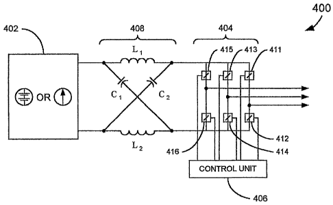
[0029] Fig. 4 depicts an electrical schematic of a Z-converter 400 that
utilizes the anti-
parallel combination of a switching device and diode for switches 411-416 of
three-phase
inverter 404. Switches 411-416 are coupled to DC source 402 by two-port
network 408
and controlled by control unit 406 to provide a desired output.
[0030] Fig. 5 shows an electrical schematic of a Z-converter 500 that uses a
reverse
blocking device or a series combination of a switching device and a diode for
switches
511-516 of three-phase inverter 504. Switches 511-516 are coupled to DC source
502 by
two-port network 508 and controlled by control unit 506 to provide a desired
output. The
DC source 502 can be virtually any power source as the impedance network 508
advantageously provides an interface that couples a load to a source
irrespective of the
[0031] function performed.
602B to realize DC source 602. According to the present invention,
implementation of
impedance circuit 608 allows the Z-converter 600, when implemented as an
inverter, to
provide an AC output voltage whose level can be adjusted to range both above
and
below the voltage level of the fuel cell stack 602A. That is, the Z-converter
600 can
function as a buck/boost inverter that has a wide range of obtainable
voltages. A three-
phase bridge 604, as is shown in Fig. 6, has nine permissible switching
states, unlike a
traditional three-phase V-converter, which has eight permissible switching
states. That
is, a traditional three-phase V-converter has six active states (vectors),
when a DC
voltage is impressed across the load, and two zero states when the load
terminals are
shorted through the lower or upper three switching devices. However, the three-
phase
Z-converter bridge has one extra zero state, which occurs when the load
terminals are
shorted through both the upper and the lower switching devices of any one
phase leg,
any two phase legs, or all three phase legs. It should be appreciated that the
zero state is
-5-
CA 02489345 2004-12-09
WO 03/107522 PCT/US03/18338
forbidden in traditional V-converters as it would cause a shoot-through
condition to
occur. As utilized herein, the third zero state is referred to as a shoot-
through zero
state. According to the present invention, the shoot-through zero state
provides a unique
buck/boost feature for the Z-converter 600.
[0032] Fig. 7 shows an equivalent circuit 700 of the Z-converter 600 with
reference to
the DC link. As is illustrated in Fig. 8, with reference to the impedance
network 608,
the bridge 604 is equivalent to a short circuit when the bridge 604 is in a
shoot-through
zero state. As is shown in Fig. 9, the bridge 604 becomes an equivalent
current source
when in one of six active states. The bridge 604 can also be represented by
current
source with a zero value (or an open circuit) when it is one of the two
traditional zero
states. Thus, Fig. 9 provides an equivalent circuit 900 for the Z-converter
600 of Fig.
6, referenced to the DC link, when the bridge 604 is in one of eight non-shoot-
through
states (i.e., six active and two zero states).
[0033] If the inductors Li and L2 and capacitors Ci and C2 have the same
inductance (L)
and capacitance (C), respectively, the Z-source network is symmetrical, and
the
equations set forth below can be utilized to further explain the operation of
the Z-
converter 600:
VC1 = VC2 = VC and 'Ll = vL2 = VL (Equations 1)
[0034] Assuming the bridge 604 is in the shoot-through zero state for a period
of To,
during a switching cycle T, the equivalent circuit of Fig. 8 yields the
following:
vL = VV , Vd = 2VC, and v; = 0 (Equations 2)
[0035] Assuming the bridge 604 is in a non-shoot-through zero state for a
period of T1,
during a switching cycle T, the equivalent circuit of Fig. 9 yields the
following:
VL = Vo - VC , vd = Vo and v, = VC - vL = 2VC - Vo (Equations 3)
where Vo is the DC source voltage and T = To + T1.
[0036] The average voltage of the inductors over one switching period (T) is
zero in the
steady state and from equations (2) and (3), we have:
VL = vL = (To = Vc +T = (V0 - VC )) /T = 0 (Equation 4)
or
VC = T (Equation 5)
Vo T1 - TO
-6-
CA 02489345 2011-04-04
100371 Similarly, the average DC link voltage across the bridge 604 is found
as follows:
T
T! _ >>; = (T0 -O + T, - (21 c -1 o )) I T = T T V0 _1 c (Equation 6)
i TO
100381 The peak DC link voltage across the bridge 604 expressed in equations
(3) can be
rewritten as:
A
v = V - VL = 2i c -10 = T, T Vo (Equation 7)
i To
with,
B T >_ 1 (Equation 8)
T,-Ta
where B is the boost factor provided by the shoot-through zero state. On the
other side,
the output peak phase voltage from the inverter can be expressed as:
A
.
vac = M - v2 (Equation 9)
where M is the modulation index. Using equation (7), equation (9) can be
further
expressed as:
V
i''ac =M - B - 2 (Equation 10)
(00391 Equation 10 illustrates that the output voltage can theoretically be
stepped-up and
stepped-down by choosing an appropriate buck-boost factor, BB, which is set
forth
below:
B 8 = M - B = (0-oo) (Equation 11)
Thus, the buck-boost factor, BB , is determined by the modulation index and
boost factor
13. which is determined by controlling the period of the shoot-through zero
state.
100401 Turning to Fig. 10, an electrical diagram of another Z-converter 1000,
which
includes a DC current source 1002 provided by a diode rectifier powered by AC
power,
is depicted. The DC current source 1002 is coupled to a bridge circuit 1004 by
an
impedance network 1008. Bridge circuit 1004 is controlled by control unit 1006
to
provide a desired output. Fig. 11 shows an electrical diagram of an equivalent
circuit
1100 of the Z-converter 1000 of Fig. 10, referred to the DC link.
100411 Fig. 12 depicts an electrical diagram of a Z-converter 1200, which
includes a DC
voltage source 1202 provided by a diode rectifier powered by an AC power
source with
an LC filter. The DC current source 1202 is coupled to a bridge circuit 1204
by an
-7-
CA 02489345 2011-04-04
impedance network 1208. Fig. 13 shows an electrical diagram of an equivalent
circuit
1300 of the Z-converter 1200, with reference to the DC link.
100421 Fig. 14 is an electrical diagram of a Z-converter 1400, which includes
a DC
voltage source 1402 provided by a battery. The DC voltage source 1402 is
coupled to a
bridge circuit 1404 by an impedance network 1408. Bridge circuit 1404 is
controlled by
a control unit 1406 to provide a desired output. Fig. 15 shows an electrical
diagram of a
Z-converter 1500 for AC-AC conversion and Fig. 16 is an electrical diagram of
a
Z-converter 1600 for DC-DC conversion. Z-converter 1600 includes a DC source
1602
that is coupled to a switch 1604 by an impedance circuit 1608. Switch 1604
comprises an
anti-parallel combination of a switching device and diode. Switch 1604 is
controlled by a
control unit 1606 to provide a desired output.
100431 Accordingly, an impedance source power converter has been described
herein,
which includes an impedance network that is configured such that the power
converter
can perform both buck and boost conversion.
100441 The above description is considered that of the preferred embodiments
only.
Modification of the invention will occur to those skilled in the art and to
those who make
or use the invention. Therefore, it is understood that the embodiments shown
in the
drawings and described above are merely for illustrative purposes and not
intended to
limit the scope of the invention, which is defined by the following claims as
interpreted
according to the principles of patent law, including the Doctrine of
Equivalents.
-8-