Note: Descriptions are shown in the official language in which they were submitted.
CA 02489567 2004-12-14
WO 2004/001857 PCT/US2002/038283
1
GE PHOTODETECTORS
PRIORITY INFORMATION
This application claims priority from provisional application Ser. No.
60/389,819 filed June 19, 2002, which is incorporated herein by reference.
BACKGROUND OF THE INVENTION
The invention relates to the field of photodetectors, and in particular to
monolithically integrated Ge photodetectors on Si.
Photodetectors are fundamental devices that convert optical signals into
electric signals. Fiber optical communication employs 1300 and 1550 nm
wavelengths because of low attenuation coefficients of silica fibers. Er doped
fiber
amplifiers emphasize the importance of 1550 nm because of the direct
amplification
of optical signals without converting to electric signals. The amplification
range
between 1530-1560 nm is referred to as C-band, and the recently extended
amplification range between 1570-1608nm is referred to as L-band. The
photodetectors for 1550 nm detection have so far been InGaAs photodetectors,
since
InGaAs is a direct semiconductor whose bandgap is 0.75 eV (corresponding to
1653nm). Thus, InGaAs photodetectors can convert any optical signal in the C-
and
L- bands to electric signals. These optical fiber communication components are
well developed.
Recently, optical technology has expanded its territory from fiber
communication to photonic integrated circuits on a chip. This allows for high
speed
and broad band communication. The impact is even larger if optics is merged
into
Si LSIs, e.g., 10 GHz clock processors, etc. InGaAs photodetectors are not
easy to
implement on a silicon chip, since InGaAs is a III-V compound semiconductor.
In
general, the elements In, Ga, and As are all dopants in silicon to show donor
or
acceptor characteristics and could thus alter the circuit performance if
diffused. Ge
can be a candidate for on-chip photodetectors, since Ge is in the group IV
element
and produces no harmful effects if diffused. Thus, Ge provides a perfect
opportunity to form highly efficient photodetectors.
SUMMARY OF THE INVENTION
According to one aspect of the invention, there is provided a photodetector
CA 02489567 2004-12-14
WO 2004/001857 PCT/US2002/038283
2
device. The photodetector device includes a plurality of Ge epilayers that are
grown
on a silicon substrate and annealed in a defined temperature range. The Ge
epilayers form a tensile strained Ge layer that allows the photodetector
device to
operate efficiently in the C-band and L-band.
According to another aspect of the invention, there is provided a method of
forming a photodetector device. The method includes forming a plurality of Ge
epilayers that are grown on a substrate. Moreover, the method includes
annealing
the Ge epilayers in a defined temperature range. Furthermore, the method
includes
developing a tensile strained Ge layer using the annealed Ge epilayers, the
tensile
strained Ge layer allowing the photodetector device to operate efficiently in
the C-
band and L-band.
According to another aspect of the invention, there is provided a
photodetector device. The photodetector device includes a plurality of Site
epilayers that are grown on a substrate at a high temperature so as to form a
Site
structure. The Site layer forms a tensile strained Site layer by cooling to
room
temperature the Site structure using the bi-metal effect. The tensile strained
Site
layer allows the photodetector device to operate efficiently in the C-band and
L-
band.
According to another aspect of the invention, there is provided a method of
forming a photodetector device. The method includes growing a plurality of
Site
epilayers on a silicon substrate at a high temperature so as to form a Site
structure.
Furthermore, the method includes forming a tensile strained Site layer by
cooling
to room temperature the Site structure using the bi-metal effect. The tensile
strained Site layer allows the photodetector device to operate efficiently in
the C-
band and L-band.
BRIEF DESCRIPTION OF TIIE DRAWINGS
FIG. 1 is schematic block diagram illustrating the techniques used to create a
Ge photodetector using a tensile strained Ge layer;
FIG. 2 is an energy band diagram of Ge under stress;
FIG. 3 is a graph of the absorption of a Ge epilayer grown using the
invention;
FIG. 4 is a graph of an optical bandgap of a Ge epilayer and a bulk Ge
CA 02489567 2004-12-14
WO 2004/001857 PCT/US2002/038283
3
analyzed using photoreflectance spectroscopy;
FIG. 5 is a graph demonstrating the tensile strain in Ge shrinking its direct
bandgap (Eg);
FIG. 6 is a X-ray locking curve measurement of the annealed tensile Ge
epilayer.
DETAILED DESCRIPTION OF THE INVENTION
Ge is an indirect semiconductor whose bandgap is 0.667 eV corresponding to
1850nm. Because of indirect bandgap characteristics, the absorption
coefficient is
small, approximately 100cni' depending on the wavelength. The direct bandgap
of
Ge is 0.8eV corresponding to 1550nm. Thus, the photodetector performance of Ge
is marginally good in the C-band but, is poor in the L-band. To overcome the
drawback of Ge, various attempts have been used, such as GeSn alloy, to
decrease
the bandgap.
One goal in Ge photodetectors is to shrink the bandgap to cover the C- and
L- bands with high efficiency. The invention uses tensile strain to accomplish
this
task.
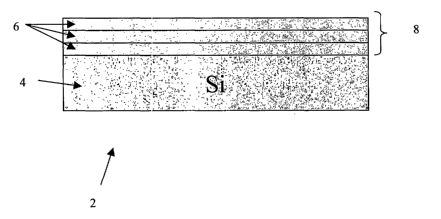
FIG. 1 is schematic block diagram illustrating the techniques used to create a
Ge photodetector 2 using a tensile strained Ge layer 8. The Ge photodetector
is
formed on a Si wafer. This is ideal for realizing Si-based optoelectronic
circuits as
well as optical interconnection in Si-LSIs. In spite of a large lattice
mismatch (4 %)
between Ge and Si, a layer 8 of Ge is grown directly on the Si wafer 4 with
uniform
thickness and with low density of threading dislocations, using an ultrahigh-
vacuum
chemical vapor deposition (UHV-CVD) technique. Other depositing techniques can
be used in accordance with this invention.
By growing the Ge layer 8 directly on the Si, the bandgap shrinkage is
shown to be induced by tensile strain. The Ge layer 8 includes a defined
number of
Ge epilayers 6, grown at 700°C on the heavily-doped p-Si (100) wafer
using the
UHV-CVD technique, which also uses GeHa (15 % in Ar) as the deposition gas.
After the growth, cyclic thermal annealing (10 cycles between 900°C and
700°C) is
performed to reduce the dislocation density. Absorption coefficients derived
from
responsibility spectra indicate substantial red shift compared with bulk Ge.
It is
shown from PR spectra that the red shift is induced by bandgap shrinkage. The
Ge
epilayers show approximately 0.77 eV, which is smaller by approximately 0.03
eV
CA 02489567 2004-12-14
WO 2004/001857 PCT/US2002/038283
4
than direct bandgap for bulk Ge. This property is beneficial for Ge
photodetectors
that can operate in the C-band as well as the L-band. The origin of the
shrinkage is
found to be not by electric-field-enhanced tunneling such as Franz-Keldysh
effect.
The pseudo potential calculation suggests that the bandgap shrinkage would
occur
under tensile strain of approximately 0.2 % . It is discussed that generation
of such
tensile strain is ascribed to the difference of thermal expansion between Ge
and Si.
Furthermore, this method is applicable for not only Ge epilayers 6, but also
Site where Ge concentration is more than 50 % to introduce thermal mismatch.
In
the case of Site, the equilibrate temperature should be designed higher than
900 °C
and preferably close to the melting temperature of the alloy. In this
embodiment, Si
is used as a substrate, however, other types of substrates can be used whose
lattice
expansion coefficient is smaller that Ge.
Another technique in creating tensile stress in Ge is to use the thermal
mismatch between Ge and Si. The linear expansion coefficients of Ge and Si are
5.8x 10⁻⁶ K-' and 2.6x 10⁻⁶ K-', respectively. When the Ge epilayers 6 are
grown on
Si and then heat up to a high temperature after growth to equilibrate these
lattices so
as to have its own lattice constants, the tensile strain should be introduced
in the Ge
epilayers 6 by cooling to room temperature the Site structure in terms of the
so
called bi-metal effect.
According to this technique, isothermal annealing at 900 °C for 10
min or
longer for Ge epilayers grown at 700 C is performed to fully relax the Ge
lattice
constant; Ge has its own lattice constant. Also isothermal annealing at 900
°C for
min or longer for Ge epilayers grown at 600 ° C is needed to fully
relax the Ge
lattice constant. Fig. 5 shows the theoretical limit of the bandgap shrinkage
using
25 the bi-metal effect. It is assumed that rapid thermal annealing is used to
cool the Ge
epilayers instantaneously to room temperature. This technique of rapid cooling
of
the Ge epilayer on Si should be more effective than slow cooling, since
lattice
relaxation could happen in slower cooling. It shows the maximum strain 0.32 %
and
the minimum bandgap 0.757 eV as shown in Fig. 2. It is marked that the bandgap
30 corresponds to 1638 nm is much longer than the long wavelength edge of the
L-
band.
Site epilayers can also be grown using this technique. The isothermal
annealing temperature can be approximately 1330 °C for Sio.sGeo.s
epilayers.
CA 02489567 2004-12-14
WO 2004/001857 PCT/US2002/038283
FIG. 2 is an energy band diagram of Ge under stress. Pseudo potential
calculations have been used. The band diagram shows that the Ge bandgap
shrinks
when tensile stress is induced. The Ge direct bandgap consists of G valley and
degenerated hole bands. When the tensile stress is introduced, the energy
position
5 of the G valley is lowered and that of the light hole band is higher,
eventually the
direct bandgap shrinks. FIG. 2 also shows that the tensile stress of 0.2 % is
needed
to shift the band edge up to 1600nm to cover the L-band. As noted above our
maximum strain is 0.32 % and the band gap is 1638 nm which should cover the L
band.
FIG. 3 is a graph of the absorption of a Ge epilayer grown using the
invention. In particular, the graph shows the absorption coefficients of the
Ge
epilayer grown using the invention and bulk Ge. Furthermore, the graph shows
increase sensitivity up to 1600nm between the C-band and L-band for the Ge
epilayer. The Ge bulk does not demonstrate increase sensitivity in the C-band
and
practically no sensitivity in the L-band. Thus, using Ge epilayers as a
tensile Ge
layer can be beneficial for operations in the C-band and L-band with
sufficient
sensitivity. Using rapid thermal annealing the Ge epilayers can be cooled
rapidly,
leading further shrinkage of the bandgap.
FIG. 4 is a graph of an optical bandgap of a Ge epilayer and a bulk Ge
analyzed using photoreflectance spectroscopy. The vertical axis is associated
with
bandgap energy and the horizontal axis is associated with the a constant value
C~=C3~ ( j-1/2)~2~2~3 , where j is an integer value that denotes the number of
peaks
and valleys in the spectrum counted from the longer wavelength. Overall, the
graph
demonstrates that a Ge epilayer grown at 700 ° C and then heated up to
900 ° C , using
the annealed steps described previously, and cooled rapidly shows a narrower
bandgap than bulk Ge. Furthermore, the graph illustrates throughout a large
span of j
values (1-5), the bandgap is consistent with a structure in the C-band and L-
band and
rarely fluctuates over the 0.75 eV bandgap. The bulk Ge structure shows a
structure
that fluctuates across a small range of j values (1-3), thus not making this
structure
useful in the C-band and L-band.
FIG. 5 is a graph demonstrating the tensile strain in Ge shrinking its direct
bandgap (Eg). The theoretical limit of Eg shrinkage is 0.757 eV corresponding
to
1638 nm, which is beyond the L-band edge (1608 nm) of Er amplifiers. The
CA 02489567 2004-12-14
WO 2004/001857 PCT/US2002/038283
6
maximum strained accumulated during the cooling process previously discussed
is
0.0032 based on the reported expansion coefficients of Ge and Si. The tensile
strain
of Ge can function as a universal photodetector for the S+C+L bands of Er
doped
amplifiers. The same properties can also be seen using a tensile strain Site
layer.
FIG. 6 is a X-ray locking curve measurement of the annealed tensile Ge
epilayer. The X-ray locking measurement includes both a tensile Ge epilayer
and an
unannealed Ge layer, and measures the wavelength of an X-ray arnving at the
sampled at a specified angle. This establishes the lattice constant of the
samples.
FIG. 5 shows that the lattice constant of the Ge epilayer is indeed larger
than bulk Ge
by 0.2 %.
Another technique to more effectively utilize the thermal mismatch in the Ge
epilayers is to grow Ge on a substrate called "Si on Quartz". Since the
lattice constant
expansion coefficient of quartz is one order of magnitude smaller than Si,
larger strain
should be accumulated in the Ge epilayers. The invention is also applicable
for
SiGeC as well.
Furthermore, another advantage of this tensile strained Ge is its light hole
band. The valence band now consists of light hole bands whose density of state
is
much smaller than the heavy hole bands. This results in lower saturation
current in
diode reverse characteristics, which are useful in photodetectors devices, and
a faster
drift velocity of holes. This is beneficial in the Ge photodetectors operating
in the
drift limited regime, not in RC limited regime. In the drift-limited regime,
the device
response time is limited by slow holes. However, light hole is as fast as
electron in
the h' point, so the response time becomes the shortest.
Although the present invention has been shown and described with respect to
several preferred embodiments thereof, various changes, omissions and
additions to
the form and detail thereof, may be made therein, without departing from the
spirit
and scope of the invention.
What is claimed is: