Note: Descriptions are shown in the official language in which they were submitted.
CA 02489796 2004-12-16
WO 2004/002006 PCT/US2003/013902
1
METIIOD FOR TUNING AN ENVELOPE TRACKING AMPLIFICATION
SYSTEM
Field of the Invention
The present invention relates generally to wireless communication devices and
in particular to an envelope tracking amplification system of a wireless
communication device.
Background of the Invention
Power amplifiers for wireless transmission applications, such as radio
frequency (RF) power amplifiers, are utilized in a wide variety of
communications
and other electronic applications. Ideally, the input-output transfer function
of a
power amplifier should be linear, that is, should implement a constant gain
adjustment
and phase adjustment of an input signal, wherein a perfect replica of the
input signal,
increased in amplitude, appears at the output of the power amplifier.
In addition, for greater efficiency, various RF systems, such as cellular
systems, attempt to run power amplifiers at or near their saturation levels,
in which
the actual output power of the amplifier is just below its maximum rated power
output
level. This power output level is generally related to the supply voltage (or
supply
power) to the power amplifier, such that a greater supply voltage will produce
a
correspondingly greater output power from the amplifier; for higher power
input
signals, a correspondingly greater actual power output is required to maintain
the
amplifier at or near saturation. In various prior art amplifiers, however, the
supply
voltage to the power amplifier is fixed. Given a typical usage situation in
which
actual power output from the amplifier may vary by a range of several orders
of
magnitude, use of a fixed supply voltage is highly inefficient, as output
power is often
an order of magnitude below its maximum, and the power amplifier is not
maintained
at or near its saturation levels.
CA 02489796 2004-12-16
WO 2004/002006 PCT/US2003/013902
2
Various techniques have evolved to vary the supply voltage to maintain the
power amplifier at or near saturation. One such technique is power supply
modulation (PSM) that varies, or modulates, the supply voltage to the power
amplifier
in order to maintain the power amplifier at or near saturation while the input
signal
varies over time. For PSM, the supply voltage of the amplifier tracks the
input signal
variations, typically utilizing a signal detector in conjunction with a
tracking power
supply. In the prior art, however, the various PSM techniques have generally
been
limited to narrowband applications, or have poor efficiency characteristics.
For example, one prior art PSM technique, known as "envelope elimination
and restoration" (EER), utilizes a limiter to provide an essentially constant
drive level
to the power amplifier to maintain the amplifier in a hard saturation state
and increase
efficiency. Use of the limiter, however, greatly expands the bandwidth of the
RF
signal input to the amplifier and requires very accurate tracking of the input
signal
envelope, with a power supply switching frequency approximately ten times
greater
than the bandwidth of the RF input signal. As these switching frequencies
increase,
the transistors within the tracking power supply become less efficient,
resulting in
excessive power losses. The resulting bandwidth expansion of the limiter also
requires the bandwidth capability .of the amplifier to be significantly
greater than the
input signal bandwidth, limiting the EER configuration to narrow bandwidth
applications, such as amplitude modulation (AM) RF broadcasts.
Another prior art P°SM technique, known as "envelope tracking,"
does not
utilize the limiter of EER. Consequently, envelope tracking power
amplification
systems may be more suitable for higher bandwidth applications. Since envelope
tracking power amplification systems modulate the supply voltage provided to
the
power amplifier, in order to maintain linearity the power amplifier of an
envelope
tracking power amplifier system must be capable of maintaining a constant gain
across varying supply voltages. Operational constraints of the envelope
tracking
power amplification system are then defined by the supply voltages at which a
specified level of gain can no longer be achieved.
CA 02489796 2004-12-16
WO 2004/002006 PCT/US2003/013902
3
Typically, envelope tracking amplification systems are tuned for optimal gain
and intermodulation distortion (IM) only at a maximum tracking power supply
voltage. The maximum tracking power supply voltage is a rated voltage, that
is, a
maximum drain (for a metal-oxide semiconductor field effect transistor
(MOSFET))
or collector (for a bipolar junction transistor) supply voltage, of a power
transistor
included in the power amplifier, which power transistor amplifies an input
signal
coupled to the envelope tracking amplification system. However, tuning at a
maximum tracking power supply voltage may yield a sub-optimal range of supply
voltages across which a constant gain may be achieved, resulting in a limited
range of
linear operation of the envelope tracking amplification system.
Therefore, there is a need for a method for tuning an envelope tracking
amplification system that results in a constant gain across a wider range of
supply
voltages than the current tuning methods, thereby producing an envelope
tracking
amplification system of improved linearity.
Brief Description of the Drawings
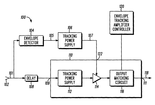
FIG. 1 is a block diagram of an envelope tracking amplification system in
accordance with an embodiment of the present invention.
FIG. 2 is a block diagram of a test system for tuning an envelope tracking
amplification system in accordance with an embodiment of the present
invention.
FIG. 3A is a logic flow diagram of steps performed by the test system of FIG.
2 in a tuning of the envelope tracking amplification system of FIG. 1 in
accordance
with an embodiment of the present invention.
FIG. 3B is a continuation of the logic flow diagram of FIG. 3A of steps
performed by the test system of FIG. 2 in a tuning of the envelope tracking
amplification system of FIG. 1 in accordance with an embodiment of the present
invention.
CA 02489796 2004-12-16
WO 2004/002006 PCT/US2003/013902
4
FIG. 4 is an exemplary, graphical representation of a relationship between an
input signal and an operating parameter for each supply voltage of multiple
supply
voltages coupled to an envelope tracking amplification system that has been
tuned at a
first supply voltage in accordance with an embodiment of the present
invention.
FIG. 5 is an exemplary, graphical representation of a relationship between an
input signal and an operating parameter for each supply voltage of multiple
supply
voltages coupled to an envelope tracking amplification system that has been
tuned at a
second supply voltage in accordance with an embodiment of the present
invention.
FIG. 6 is a logic flow diagram of steps performed by the test system of FIG. 2
in a tuning of the envelope tracking amplification system of FIG. 1 in
accordance with
another embodiment of the present invention.
Detailed Description of the Invention
To address the need for a method for tuning an envelope tracking
amplification system that results in a constant gain across a wider range of
supply
voltages than the current tuning methods, thereby producing an envelope
tracking
amplification system of improved linearity, an optimal operating point of an
envelope
tracking amplification system that includes a radio frequency (RF) power
amplifier
having an RF amplifying element is determined based on an application to the
RF
power amplifier of a supply voltage that is less than the rated voltage of the
RF
amplifying element.
Generally, one embodiment of the present invention encompasses a method
for tuning an RF power amplifier. The method includes steps of determining a
preferred operating point for the RF power amplifier for each supply voltage
of a first
set of supply voltages to produce multiple preferred operating points and, for
each
preferred operating point of the multiple preferred operating points,
determining, for
each supply voltage of a second set of supply voltages, a relationship between
an
operating parameter of the RF power amplifier and a signal coupled to an input
of the
RF power amplifier to produce multiple relationships associated with the
preferred
operating point. The method further includes steps of, for each preferred
operating
CA 02489796 2004-12-16
WO 2004/002006 PCT/US2003/013902
point of the multiple preferred operating points, determining a range of
acceptable
operation of the RF power amplifier based on the multiple relationships
associated
with the preferred operating point and comparing the range of acceptable
operation
determined with respect to each preferred operating point of the multiple
preferred
5 operating points to the ranges of acceptable operation determined with
respect to the
other preferred operating points of the multiple preferred operating points to
produce
at least one comparison. The method further includes a step of determining an
optimal operating point based on the at least one comparison.
Another embodiment of the present invention encompasses a method for
tuning an envelope tracking amplification system having a radio frequency (RF)
power amplifier. The method includes steps of determining an operating point
for
each supply voltage of multiple supply voltages to produce multiple operating
points
and setting a first operating point of the multiple operating points. The
method
further includes steps of, in response to setting the first operating point,
coupling a
first supply voltage to the RF power amplifier, coupling a first input signal
to an input
of the RF power amplifier, amplifying the first input signal to produce a
first
amplified signal, and measuring an operating parameter of the RF power
amplifier
based on the first amplified signal to produce a first operating parameter
measurement. The method further includes steps of, in response to setting the
first
operating point, coupling a second supply voltage to the RF power amplifier,
coupling
a second input signal to the input of the RF power amplifier, amplifying the
second
input signal to produce a second amplified signal, and measuring an operating
parameter of the RF power amplifier based on the input signal and the second
amplified signal to produce a second operating parameter measurement.
The method further includes steps of setting a second operating point of the
multiple operating points and, in response to setting the second operating
point,
coupling the first supply voltage to the RF power amplifier, coupling a third
input
signal to the input of the RF power amplifier, amplifying the third input
signal to
produce a third amplified signal, and measuring an operating parameter of the
RF
power amplifier based on the third amplified signal to produce a third
operating
CA 02489796 2004-12-16
WO 2004/002006 PCT/US2003/013902
6
parameter measurement. The method further includes steps of, in response to
setting
the second operating point, coupling the second supply voltage to the RF power
amplifier, coupling a fourth input signal to an input of the RF power
amplifier,
amplifying the fourth input signal to produce a fourth amplified signal, and
measuring
an operating parameter of the RF power amplifier based on the fourth amplified
signal
to produce a fourth operating parameter measurement. The method further
includes a
step of determining an optimal operating point based on the first operating
parameter
measurement, the second operating parameter measurement, the third operating
parameter measurement, and the fourth operating parameter measurement.
Yet another embodiment of the present invention encompasses a method for
tuning an envelope tracking amplification system that includes a RF power
amplifier
having an RF amplifying element. The method includes steps of coupling a
predetermined supply voltage to the RF power amplifier, wherein the
predetermined
supply voltage is less than a rated voltage of the RF amplifying element and
determining a preferred operating point for the RF power amplifier based on
the
predetermined supply voltage.
The present invention may be more fully described with reference to FIGS. 1-
6. FIG. 1 is a block diagram of envelope tracking amplification system 100 in
accordance with an embodiment of the present invention. Envelope tracking
amplification system 100 includes an input 102 coupled to each of an envelope
detector 104 and a radio frequency (RF) power amplifier 110. Envelope tracking
amplification system 100 further includes a tracking power supply 106 coupled
to the
envelope detector and further coupled to RF power amplifier 110. Envelope
tracking
amplification system 100 may further include a delay circuit 108 interposed
between
input 102 and RF power amplifier 110. Delay circuit 108 is utilized to delay,
and
thereby synchronize, a version of input signal 101 that is applied to RF power
amplifier 110 with a corresponding control signal 107 that is sourced by
tracking
power supply 106 to the RF power amplifier.
RF power amplifier 110 includes an RF input 109, a supply voltage input 122,
and an output 111 and further includes at least one RF amplifying element 114
such
CA 02489796 2004-12-16
WO 2004/002006 PCT/US2003/013902
7
as a power transistor, preferably a lateral drain metal-oxide semiconductor
(LDMOS)
transistor, an input matching circuit 112, an output matching circuit 116, and
biasing
and decoupling circuitry as are necessary to allow the functionality of the RF
amplifying element and to bias the RF amplifying element class AB; however,
those
of ordinary skill in the art realize that other biases, such as classes A, B,
or C, may be
used here without departing from the spirit and scope of the present
invention.
In one embodiment of the present invention, output matching circuit 116
includes an adjustable load circuit. Adjustable load circuits are well known
in the art
and will not be described in detail. For example, an adjustable load circuit
whose
load impedance may be adjusted in response to a control signal is described in
detail
in LT.S. patent number 5,060,294, entitled "Dual Mode Power Amplifier for
Radiotelephone," which patent is assigned to the assignee of the present
invention and
is hereby incorporated by reference herein in its entirety. An envelope
tracking
amplification system controller 120 controls the adjustable load circuit,
thereby
controlling an output impedance presented to RF amplifying element 114. By
adjusting an impedance of output matching circuit 116, envelope tracking
amplification system controller 120 is, able to effectuate a desired operating
point for
RF power amplifier 110. By efFectuating a desired operating point for RF power
amplifier 110, envelope tracking amplification system controller 120 can
control the
gain applied to an amplified signal and the distortion components introduced
to the
amplified signal by RF power amplifier 110.
In yet another embodiment of the present invention, output matching circuit
116 may include multiple, parallel load circuits and a multiple output
switching
device, such as a demultiplexer or multiple RF switching devices such as PIN
diodes
or GASFET switches, that is coupled between each load circuit of the multiple,
parallel load circuits and RF amplifying element 114. The multiple output
switching
device is further coupled to envelope tracking amplification system controller
120,
which, by controlling the multiple output switching device, controls which
load
circuit of the multiple load circuits is coupled to RF amplifying element 114.
By
selecting a load circuit from among the multiple load circuits for coupling to
RF
CA 02489796 2004-12-16
WO 2004/002006 PCT/US2003/013902
8
amplifying element 114, envelope tracking amplification system controller 120
is
again able to control the output impedance presented to the RF amplifying
element
and to effectuate a desired operating point for RF power amplifier 110.
Envelope tracking amplification system 100 operates as follows. An RF
signal 101 comprising carrier components is input into envelope tracking
amplification system 100. Envelope tracking amplification system 100 routes
input
signal 101 to envelope detector 104. Envelope detector 104 tracks or detects
an
envelope of input signal 101 to produce an envelope detector signal 105,
typically a
voltage. A tracking power supply 106 is then utilized to further track (or
quantize) the
envelope detector voltage or signal 105 and to adjust a control signal 107
that is based
on the envelope of input signal 101 and is sourced by the tracking power
supply to RF
power amplifier 110.
In one embodiment of the present invention, control signal 107 is a supply
voltage sourced to RF power amplifier 110. By tracking input signal 101,
envelope
detector 104 and tracking power supply 106 provide a variable supply voltage
107 to
RF power amplifier 110 and enable the main amplifier to be maintained at or
near
saturation over a wide range of magnitudes of input signal 101, thereby
providing for
highly efficient amplification of the input signal.
Typically, in the prior art, an RF power amplifier portion of an envelope
tracking amplification system is tuned for optiW al gain, phase shift, and/or
intermodulation distortion (IM) at a rated supply voltage of a RF amplifying
element
included in the amplification system. For example, RF amplifying element 114
may
be an MRF286 power transistor or a MRF187,power transistor, each available
from
Motorola, Inc., of Schaumburg, Illinois. MRF286 is a 26 volt (V) part, that
is, is rated
for a supply voltage of 26V, and MRF 187 is a 27 volt (V) part. As a result,
an
envelope tracking amplification system of the prior art having an RF power
amplifier
that includes an MRF 187 power transistor is tuned by coupling a supply
voltage of
27V to the envelope tracking amplification system and then effectuating a
desired
operating point for the amplification system based on the 27V supply voltage.
CA 02489796 2004-12-16
WO 2004/002006 PCT/US2003/013902
9
In order to maximize an operating efficiency of envelope tracking
amplification system 100 and to provide acceptable operation of the
amplification
system across the widest range of supply voltages during operation of the
amplification system, such as providing a constant gain, that is, gain
flatness, over the
widest range of supply voltages, a supply voltage that is used to tune RF
power
amplifier 110 of envelope tracking amplification system 100 is dynamically
selected
during a tuning process. FIG. 2 is a block diagram of a test system 200 for a
tuning of
envelope tracking amplification system 100, and in particular RF power
amplifier
110, in accordance with an embodiment of the present invention. Test system
200
includes a signal generator 202 that is coupled to input 109 of RF powe~
amplifier 110
and that sources at least one test signal 203 to the RF power amplifier to
produce at
least one amplified signal 205. Test system 200 further includes a signal
measurement device 204 that measures an operating parameter associated with
the at
least one amplified signal 205, and a load 206 to receive the at least one
amplified
signa1205.
Those who are of ordinary skill in the art realize that test system 200 can be
either a physical test system or a simulated test system. For example, test
system 200
may be set up in a factory or an envelope tracking amplification system design
laboratory using discrete hardware components. By way of another example, test
system 200 may be implemented in a computer aided design (CAD) system and may
be utilized as part of a computer simulation design process for determining an
optimal
design of an envelope tracking amplification system, and in particular an RF
power
amplifier. For example, test system 200 may be utilized as part of a
simulation
process to determine optimal values for components of an output matching
circuit of
the RF power amplifier, which component values can then be implemented in a
hardware version of the output matching circuit.
Test system 200 further includes a test system controller 208 that is operably
coupled to, and controls, signal generator 202 and measurement device 204 and
that
stores their respective readings. Alternatively, the functions described
herein of test
system controller 208 may be performed by envelope tracking system controller
120.
CA 02489796 2004-12-16
WO 2004/002006 PCT/US2003/013902
Test system controller 208 further may be operably coupled to RF power
amplifier
110 and may control an adjustment of a load presented by output matching
circuit 116
to RF amplifying element 114. Test system 200 further includes a variable
voltage
power supply 210 that is coupled to supply voltage input 122 of RF power
amplifier
5 110 and is further coupled to, and controlled by, test system controller
208. Variable
voltage supply 210 performs the function of tracking power supply 106 during
the
tuning process by sourcing a supply voltage 211 to RF power amplifier 110.
Alternatively, the functions described herein of variable voltage supply 210
may be
performed by tracking power supply 106.
10 Preferably, signal measurement device 204 is a power meter that measures a
power of the at least one amplified signal 205. However, those who are of
ordinary
skill in the art realize that the type of measurement device comprising signal
measurement device 204 depends upon the operating parameter being measured.
For
example, in another embodiment of the present invention, wherein the operating
parameter being measured is distortion introduced to an amplified signal by
amplification system 100, measurement device 204 may comprise a spectrum
analyzer or a phase analyzer coupled to, or implemented in, controller 208.
FIGS. 3A and 3B are a logic flow diagram 300 of steps performed by test
system 200 in tuning RF power amplifier 110 in accordance with an embodiment
of
the present invention. As noted above, envelope tracking amplification system
100 is
designed to operate over a range of supply voltages. Logic flow 300 begins
(302)
when test system 200 determines (304) a preferred operating point for envelope
tracking amplification system 100 for each supply voltage of a first set of
supply
voltages, thereby producing multiple preferred operating points.
In one embodiment of the present invention, a preferred operating point
associated with each supply voltage of the first set of supply voltages may be
predetermined by the designer of RF power amplifier 110 and stored in
controller
208. In another embodiment of the present invention, a determination of a
preferred
operating point for each supply voltage of the first set of supply voltages
may include
the following steps. Variable voltage power supply 210 couples a first supply
voltage
CA 02489796 2004-12-16
WO 2004/002006 PCT/US2003/013902
11
of the first set of supply voltages to RF amplifying element 114 of RF power
amplifier 110. In addition, signal generator 202 generates at least one test
signal 203
that is coupled to input 109 of RF power amplifier 110. Test system controller
208
adjusts output matching circuit 116 in order to adjust an output impedance
presented
to RF amplifying element 114 and thereby an operating point of RF amplifying
element 114. RF amplifying element 114 amplifies the at least one test signal
based
on the adjusted operating point to produce at least one amplified signal.
Measurement
device 204 measures an operating parameter, such as gain, phase, or IM, of RF
power
amplifier 110 based on the at least one amplified signal and the adjusted
operating
point. Test system controller 208 then determines a preferred operating point
associated with the first supply voltage by selecting an operating point
corresponding
to an optimal measured operating paxameter.~
Preferably, the preferred operating point is an operating point of RF
amplifying element 114 that yields an optimal operating parameter. When the at
least
one test signal is applied to RF power amplifier 110, and via input matching
circuit ,'
112 to RF amplifying element 114, test system controller 208 adjusts an
operating
point of RF amplifying element 114 by adjusting the output impedance presented
to
the RF amplifying element. Controller 208 then determines an optimal operating
point that corresponds to the optimal operating parameter as measured by
measurement device 204.
A second supply voltage of the first set of supply voltages is then sourced to
RF power amplifier 110 and signal generator 202 again generates at least one
test
signal 203 that is also coupled to the RF power amplifier. In response to the
coupling
of the second supply voltage and the coupling of at least one test signal 203
to RF
power amplifier 110, test system controller 208 determines a preferred
operating point
associated with the second supply voltage. The above process continues until a
preferred operating point is determined for each supply voltage of the first
set of
supply voltages, thereby producing multiple preferred operating points.
In one embodiment of the present invention, the at least one test signal may
be
set at multiple power levels, such as a swept power signal or signals, or may
be set at
CA 02489796 2004-12-16
WO 2004/002006 PCT/US2003/013902
12
a single power level, such as a lower end, a mid-range, or an upper end of a
specified
input signal power range of RF power amplifier 110. Test system controller 208
then
optimizes an operating parameter of RF power amplifier 110 by adjusting output
matching circuit 116 of the RF power amplifier in response to receipt of the
test
signal. In another embodiment of the present invention, the at least one test
signal
may comprise multiple test signals, wherein each test signal of the multiple
test
signals is at a same power level, but at a different frequency, than the other
test
signals of the multiple test signals. Test system controller 208 then
optimizes an
operating parameter of RF power amplifier 110 by adjusting output matching
circuit
116 such that the operating parameter is optimized across each of the multiple
test
signal frequencies or such that the operating parameter attains a
predetermined
operating parameter threshold, which threshold is stored in the controller, at
each of
the multiple test signal frequencies.
Upon determining the multiple preferred operating points, test system' 200,
preferably test system controller 208, then sets (306) a first preferred
operating point
of the multiple preferred operating points for RF power amplifier 110,
preferably by
adjusting output matching circuit 116 of the RF power amplifier. In addition,
test
system 200, preferably variable voltage power supply 210, couples (308) to RF
power
amplifier 110 a first supply voltage of a second set of supply voltages. The
second set
of supply voltages may be the same as the first set of supply voltages.
However,
those who are of ordinary skill in the art realize that the second set of
supply voltages
may differ the first set of supply voltages without departing from the spirit
and scope
of the present invention. In addition, test system 200, preferably signal
generator 202,
couples (310) at least one test signal to input 109 of RF power amplifier 110,
which at
least one test signal may or may not be the same as the at least one test
signal utilized
to determine the multiple preferred operating points.
Based on the coupled supply voltage of the second set of supply voltages, RF
power amplifier 110 amplifies (312) the at least one test signal to produce at
least one
amplified signal. Test system 200, preferably measurement device 204 in
conjunction
with controller 208, then measures (314) an operating parameter of RF power
CA 02489796 2004-12-16
WO 2004/002006 PCT/US2003/013902
13
amplifier 110 based on the at least one amplified signal. For example, test
system 200
may measure an output power of the at least one amplified signal, a gain or a
phase
shift of the at least one amplified signal relative to the corresponding test
signal, or a
distortion, such as IM, introduced to the at least one amplified signal by RF
power
amplifier 110. Test system 200, preferably controller 208, then determines
(316) a
relationship between the at least one test signal, preferably a power
associated with
the at least one test signal, and the corresponding operating parameter
measurements,
and stores (318) information related to the determined relationship, such as
data
points or an algorithm describing a curve that defines the relationship.
Test system 200, preferably controller 208, then determines (320) whether
each supply voltage of the second set of supply voltages has been coupled to
RF
power amplifier 110. When test system 200 determines that at least one supply
voltage of the second set of supply voltages has not yet been coupled to RF
power
amplifier 110, test system 200, preferably variable voltage power supply 210,
couples
(322) one of the remaining, not yet coupled, supply voltages included in the
second
set of supply voltages to RF power amplifier 110 and repeats steps (310)-
(320).
When test system 200 determines that each supply voltage of the second set of
supply voltages has been coupled to RF power amplifier 110, test system 200,
preferably test system controller 208, determines (324) an acceptable range of
operation with respect to the set operating point. The determination of the
acceptable
range of operation is based on the relationship determined between the at
least one
test signal and the corresponding operating parameter measurements for each
supply
voltage of the second set of supply voltages. The acceptable range of
operation
describes the range of supply voltages over which RF power amplifier 110 is
able to
attain an acceptable operating parameter level.
For example, FIGS. 4 and 5 depict an acceptable range of operation, that is, a
range of supply voltages capable of providing a constant gain, for each of two
different operating points of an RF power amplifier such as RF power amplifier
110.
The RF power amplifier underlying each of FIGS. 4 and 5 includes an MRF187
power
transistor, available from Motorola, Inc., of Schaumburg, Illinois, as the RF
CA 02489796 2004-12-16
WO 2004/002006 PCT/US2003/013902
14
amplifying element included in the RF power amplifier. MRF187 is a 27 volt (V)
part, that is, is rated for a maximum supply voltage of 27V. FIG. 4 graphs
data
produced by the RF power amplifier when tuned to a preferred operating point
at the
rated supply voltage of the RF amplifying element, that is, at 27V. FIG. 5
graphs data
produced by the RF power amplifier when tuned to a preferred operating point
at a
lower supply voltage, that is, at 17V.
FIG. 4 is a graphical representation 400 of a relationship between input
signal
power and gain for the RF power amplifier when tuned to a preferred operating
point
at 27V. A horizontal axis 401 of graph 400 depicts a power level (in dBm) of
an
input signal applied to the RF power amplifier, and a vertical axis 402
depicts a power
gain (in decibels, or dB) of a signal output by the RF power amplifier in
response to
the application of the input signal. FIG. 4 further depicts multiple curves
404-409,
wherein each curve 404-409 graphs a relationship between an input signal, that
is, a
power of the input signal, and an operating parameter, that is, a gain of the
amplification system, for one of multiple supply voltages (six shown). As
depicted in
FIG. 4, the curves 404-409 respectively correspond to coupled supply voltages
of 27
volts (V), 24V, 21V, 18V, 15V, and 12V.
As can be seen by FIG. 4, the variation in gain among the multiple supply
voltage curves 404-409 is sufficiently dramatic that the RF power amplifier
can
maintain a constant gain (i.e., a constant gain trajectory) across only a very
limited
range of supply voltages. That is, the RF power amplifier depicted in FIG. 4
is able to
achieve a constant gain, of approximately l4dB, only for supply voltages from
21 V to
27V. For supply voltages of less than 21V, the RF power amplifier is unable to
attain
a gain of approximately l4dB regardless of the input power level, while for a
supply
voltage of 27V the RF power amplifier is unable to reduce its gain much below
l4dB
regardless of the input power level. Thus an acceptable range of operation for
the RF
power amplifier tuned at 27V is a supply voltage range of 21 V to 27V.
FIG. 5 is a graphical representation 500 of a relationship between input
signal
power and gain for the RF power amplifier when tuned to a preferred operating
point
at 17V. Similar to FIG. 4, a horizontal axis 501 of graph 500 depicts a power
level (in
CA 02489796 2004-12-16
WO 2004/002006 PCT/US2003/013902
dBm) of an input signal applied to the RF power amplifier, and a vertical axis
502
depicts a power gain (in dB) of a signal output by the RF power amplifier in
response
to the application of the input signal. FIG. 5 further depicts multiple curves
504-510,
wherein each curve 504-510 graphs a relationship between an input signal, that
is, a
5 power of the input signal, and an operating parameter, that is, a gain of
the RF power
amplifier, for one of multiple supply voltages (seven shown). As depicted in
FIG. 5,
the curves 504-510 respectively correspond to applied supply voltages of 27
volts (V),
24V, 21V, 18V, 15V, 12V, and 9V.
As shown in FIG. 5, for each supply voltage from 15V to 27V, there exists
10 some input signal power level in the range from approximately lSdBm to
approximately 35dBm for which the RF power amplifier is able to achieve a gain
of
approximately lSdB. That is, FIG. 5 depicts an RF power amplifier that is able
to
maintain a constant gain (i.e., a constant gain trajectory) across supply
voltages
ranging from 15V to 27V. Thus an acceptable range of operation for the RF
power
15 amplifier tuned at 17V is a supply voltage range of 15V to 27V.
Referring again to FIG. 3, when test system 200 determines that each supply
voltage of the second set of supply voltages has been coupled to RF power
amplifier
110, test system 200, preferably test system controller 208, further
determines (326)
whether each operating point of the multiple preferred operating points has
been set
for RF power amplifier 110. When test system 200 determines that at least one
operating point of the multiple preferred operating points has not been set
for RF
power amplifier 110, test system 200, preferably controller 208, sets (328)
one of the
remaining, not yet set, operating points of the multiple preferred operating
points for
RF power amplifier 110. Test system 200 then repeats steps (308)-(326).
When test system 200, preferably test system controller 208, determines that
each operating points of the multiple preferred operating points has been set
for RF
power amplifier 110, test system 200, preferably test system controller 208,
compaxes
(330) the acceptable range of operation determined for each operating point of
the
multiple preferred operating points to the acceptable ranges of operation
determined
for the other operating points of the multiple preferred operating points to
produce at
CA 02489796 2004-12-16
WO 2004/002006 PCT/US2003/013902
16
least one comparison. Test system 200, preferably test system controller 208,
then
determines (332) an optimal operating point based on the at least one
comparison.
Based on the determined optimal operating point, test system 200, preferably
test
system controller 208, can determine (334) an optimal supply voltage for a
tuning of
RF power amplifier 110, which preferably is the supply voltage associated with
the
optimal operating point. Logic flow 300 then ends (336). The optimal operating
point may then be implemented in RF power amplifier 110.
For example, referring again to FIGs. 4 and 5, FIG. 4 depicts an acceptable
range of operation, that is, a range of supply voltages over which a constant
gain can
achieved (i.e., a constant gain trajectory), for an operating point that is
set when an RF
power amplifier is tuned at a supply voltage of 27V. The acceptable range of
operation depicted by FIG. 4 is a supply voltage of 21 V to 27V. FIG. 5
depicts an
acceptable range of operation, that is, a supply voltage range of 15V to 27V,
when the
RF power amplifier is tuned at a supply voltage of 17V. A comparison of the
acceptable ranges of operation represented by the graphs depicted in each of
FIGS. 4
and 5 indicates that the operating point determined when the RF power
amplifier is
tuned at a supply voltage of 17V provides a wider acceptable range of
operation, that
is, a wider constant gain trajectory, than the operating point determined when
the RF
power amplifier is tuned at the rated supply voltage of 27V. Therefore, again
referring to FIGs. 4 and 5, an optimal operating point based on the comparison
of the
acceptable ranges of operation represented therein would be the operating
point
corresponding to a tuning of the RF power amplifier at a supply voltage of
17V.
In general, tuning system 200 tunes RF power amplifier 110 at each of
multiple supply voltages to determine a preferred operating point
corresponding to
each supply voltage. Tuning system 200 then determines an acceptable range of
operation corresponding to each preferred operating point by setting RF power
amplifier 110 at the preferred operating point and testing a performance of
the RF
power amplifier across a range of supply voltages. Tuning system 200 then
compares
the acceptable ranges of operation determined with respect the preferred
operating
points and determines an acceptable range of operation, and a corresponding
preferred
CA 02489796 2004-12-16
WO 2004/002006 PCT/US2003/013902
17
operating point, that yields the optimal performance. As a result, by tuning
RF power
amplifier 110 supply voltages that are less than a rated supply voltage of RF
amplifying element 114, test system 200 is able to determine an optimal
operating
point with a broader range of acceptable operation than the prior art.
In another embodiment of the present invention, RF power amplifier 110 may
be tuned by test system 200 without determining a preferred operating point
for each
of multiple supply voltages. As depicted in FIGs. 4 and 5, improvements in
linearity
of an RF power amplifier can be achieved by tuning the RF power amplifier,
that is,
by determining an optimal operating point based on adjustments of an output
match of
an RF amplifying element of the RF power amplifier, at a supply voltage that
is '~
significantly lower than the rated, or maximum, voltage of the RF amplifying
element. Therefore, instead of determining a preferred operating point for
each of
multiple supply voltages, a tuning voltage that is less than the rated, or
maximum,
voltage of the RF amplifying element may be predetermined.
FIG. 6 is a logic flow diagram 600 of a method for tuning RF power amplifier
110 without determining a preferred operating point for each of multiple
supply
voltages. Logic flow diagram 600 begins (602) when test system 200, preferably
variable voltage supply 210, couples (604) a predetermined supply voltage to
RF
power amplifier 110. The predetermined supply voltage is less than a rated
voltage of
RF amplifying element 114. Test system 200 then determines (606) a preferred
operating point for RF power amplifier 110 based on the predetermined supply
voltage, and the logic flow ends (608).
Preferably, the step of determining (604) a preferred operating point includes
the following steps. Test system 200, preferably signal generator 202, couples
at least
one test signal to RF power amplifier 110. Test system controller 208 adjusts
output
matching circuit 116 in order to adjust an output impedance presented to RF
amplifying element 114 and thereby an operating point of the RF amplifying
element
114. RF amplifying element 114 amplifies the at least one test signal based on
the
adjusted operating point to produce at least one amplified signal. Measurement
device 204 measures an operating parameter, such as gain, phase, or IM, of RF
power
CA 02489796 2004-12-16
WO 2004/002006 PCT/US2003/013902
18
amplifier 110 based on the at least one amplified signal and the adjusted
operating
point. Test system controller 208 then determines a preferred operating point
associated with the predetermined supply voltage by selecting an operating
point
corresponding to an optimal measured operating parameter.
Preferably, when the RF amplifying element of the RF power amplifier, such
as RF amplifying element 114 of RF power amplifier 110, is biased class B, the
optimal tuning supply voltage has the same relationship to the rated, or
maximum,
voltage of the RF amplifying element as the average power of amplified signals
produced by the RF power amplifier 110 has to the maximum linear output power,
that is, to a power level corresponding to a 1dB gain compression point. For
example,
if the average power output by the RF power amplifier during a course of
normal
operation is 7dB backed off from a power level corresponding to a 1 dB gain
compression point, the supply voltage used to tune up the RF power amplifier
is~
approximately Vrated~Sqrt(5), that is, the rated voltage divided by the square
root. of 5:
In the case of an RF amplifying element with a rated voltage of 26V, the
supply
voltage used to tune the RF power amplifier for class B operation would be
approximately 11-12V. Similarly, an optimal tuning supply voltage for class AB
operation is also less than the rated voltage of the RF amplifying element, as
shown iri
FIGS. 4 and 5, although likely a higher percentage of the rated voltage of the
RF
amplifying element than the class B tuning voltage due to the more linear bias
and
other considerations as non-linear junction capacitances, non-linear
transconductance
gm, non-zero saturated voltages, and so on. Optimal tuning supply voltages for
other
classes of operation can be determined and set by the designer of the RF power
amplifier.
In sum, by tuning RF power amplifier 110 at at least one supply voltage that
is
less than a rated supply voltage of RF amplifying element 114, test system 200
is able
to determine an optimal operating point with a broader range of acceptable
operation
than the prior art. The implementation of the optimal operating point in
envelope
tracking amplification system 100 produces an amplification system of improved
linearity over the amplification systems of the prior art.
CA 02489796 2004-12-16
WO 2004/002006 PCT/US2003/013902
19
While the present invention has been particularly shown and described with
reference to particular embodiments thereof, it will be understood by those
skilled in
the art that vaxious changes may be made and equivalents substituted for
elements
thereof without departing from the scope of the invention as set forth in the
claims
below. Accordingly, the specification and figures are to be regarded in an
illustrative
rather then a restrictive sense, and all such changes and substitutions are
intended to
be included within the scope of the present invention.
Benefits, other advantages, and solutions to problems have been described
above with regard to specific embodiments. However, the benefits, advantages,
solutions to problems, and 'any elements) that may cause any benefit,
advantage, or
solution to occur or become more pronounced are not to be construed as a
critical,
required, or essential feature or element of any or all the claims. As used
herein, the
terms "comprises," "comprising," or any variation thereof, are intended to
cover a
non-exclusive inclusion, such that a process, method, article, or apparatus
that
comprises a list of elements does not include only those elements but may
include
other elements not expressly listed or inherent to such process, method,
article, or
apparatus.