Note: Descriptions are shown in the official language in which they were submitted.
CA 02490074 2004-12-20
WO 2004/000728 PCT/JP2003/005628
-1-
METHOD FOR MAKING CARBON NANOTUBES
TECHNICAL FIELD
The present invention relates to a method for making carbon film for use in
small fuel cells, and in particular to a method for forming a carbon nanotube
(CNT) on
an electroconductive member.
BACKGROUND OF THE INVENTION
A carbon nanotube consists of a cylindrical tube made of carbon and is
provided with a diameter in the order of nanometers owing to certain desirable
properties thereof. Japanese patent laid open publication No. 2000-141084, for
instance,
discloses the use of carbon film consisting of a carbon nanotube as a carrier
for
platinum or other catalyst. As a carbon nanotube is highly porous, it can
serve as a gas
diffusion layer. In the invention disclosed in this patent publication, a
carbon nanotube
film is formed on an iron or nickel film which is in turn formed on an
electrode terminal
layer made of gold or the like, and a platinum catalyst is sputtered onto the
surface of
this carbon nanotube film.
There are other methods for forming a carbon nanotube which use electric arc
discharge and heating. Japanese patent laid open publication No. 2001-58805,
for
instance, discloses a method for making carbon nanotube in a large volume and
in a
simple manner by mixing fullerene molecules with a transition element or an
alloy
containing a transition element, and heating the mixture on a ceramic board.
However,
this patent publication contains no mentioning of the formation of a carbon
nanotube on
an electroconductive member.
It is known to use a transition metal such as iron and nickel in a fine
particle
form as a catalyst for forming a carbon nanotube. Such fine metallic particles
can be
prepared by etching metallic film using laser or microwave and filling
metallic film into
CA 02490074 2007-09-20
2
the pores of zeolite and porous silicon.
BRIEF SUMMARY OF THE INVENTION
In view of such problems of the prior art, a primary object of the present
invention is to provide an improved method for forming a carbon nanotube on an
electroconductive member.
A second object of the present invention is to provide a method for forming a
carbon nanotube which allows fine metallic particles that can be used as a
catalyst for
growing a carbon nanotube to be prepared in a simple, economical and efficient
manner.
A third object of the present invention is to provide a method for forming a
carbon nanotube which is suitable for use in fuel cells.
The present invention accomplishes such objects by providing a method for
making a carbon nanotube on an electroconductive member, comprising the steps
of:
forming a first electroconductive layer on a silicon substrate, where the
first
electroconductive layer is formed of a member selected from a group consisting
of Ti,
Ni, Al and Cr;
forming a second electroconductive layer on the first electroconductive layer,
the second electroconductive layer is formed of a member selected from a group
consisting of W, Mo and Ta;
forming a catalytic layer including a metal or alloy that serves as a catalyst
for
growing the carbon nanotube on the second electroconductive layer;
processing the metal or alloy of the catalytic layer so as to turn it into
small
particles having a particle size of 0.5 to 50 nm; and
growing the carbon nanotube on the second electroconductive layer by using
the small particles of the metal or alloy of the catalytic layer as the
catalyst;
wherein the step of processing the metal or alloy of the catalytic layer so as
to
turn it into small particles comprises the step of heating the catalytic layer
formed on
the second electroconductive layer while supplying inert gas. Thereby, fine
metallic or
alloy particles that can be used as a catalyst for growing a carbon nanotube
can be
prepared in a simple, economical and efficient manner, and a carbon nanotube
can be
efficiently formed on the electroconductive member by using it as a catalyst.
The catalytic layer may comprise a member selected from a group consisting
of Fe, Ni, Co, Mo and an alloy thereof.
CA 02490074 2007-09-20
-3-
The inert gas may consist of helium or argon.
The prescribed temperature may be in range of 0.49Tm to 0.59Tm where Tm is
the melting point of the metal or alloy of the catalytic layer in Kelvin. When
the
catalytic layer is made of iron, the prescribed temperature may be
approximately 700 C.
If the heating temperature is higher or lower than this, the particles tend to
become
coarser, and a desired particle size cannot be obtained. The small particles
of the metal
or alloy preferably have a particle size of 0.5 to 50 nm. Particles of such a
size provides
an adequate catalytic action in forming a carbon nanotube, and can be easily
obtained
by the method described above. By turning the metal or alloy of the catalytic
layer into
small particles at such a heating temperature, particles of a desired size can
be obtained
both easily and efficiently.
The step of growing the carbon nanotube may comprise the step of supplying
mixed gas containing hydrocarbon gas and the inert gas at a ratio of 1:2 to
1:50 so that
amorphous carbon other than a carbon nanotube or soot may be avoided and a
carbon
nanotube may be formed in an efficient manner without the growth rate thereof
being
hampered to any great extent.
The step of supplying the mixed gas may be conducted at a flow rate of 1 to
100 cm/min, and more preferably at a flow rate of approximately 30 cm/min.
Thereby,
the productivity can be improved by controlling the formation of soot and
reducing the
amount of the material gas that is expelled without contributing to the
fonnation of the
carbon nanotube. When the step of growing the carbon nanotube comprises the
step of
placing the electroconductive member including the small particles of the
metal or alloy
in a tube having an inner diameter of approximately 30 mm, the flow rate of
the mixed
gas that is flowed substantially along the length of the tube is preferably in
the order of
CA 02490074 2004-12-20
WO 2004/000728 PCT/JP2003/005628
-4-
200 to 300 sccm (standard cubic centimeter per minute).
The electroconductive member may be deposited on an inorganic substrate
made of such material as silicon or glass. The electroconductive member may
have a
two-layered structure including a titanium (Ti) layer and a tungsten (W) layer
formed
thereon. Instead of titanium, aluminum (Al), nickel (Ni) or chromium (Cr) can
also be
used. Instead of tungsten, molybdenum (Mo) or tantalum (Ta) can also be used.
BRIEF DESCRIPTION OF THE DRAWINGS
Now the present invention is described in the following with reference to the
appended drawings, in which:
Figure 1 is a flowchart describing the preferred embodiment of the method for
forming a carbon nanotube film according to the present invention;
Figures 2a to 2e are schematic sectional views illustrating an exemplary
method for forming a carbon nanotube film according to the present invention;
Figure 3 is a schematic sectional view of the device for forming a carbon
nanotube film that can be used for implementing the present invention;
Figure 4a to 4e are schematic sectional views illustrating another exemplary
method for forming a carbon nanotube film according to the present invention;
and
Figures 5a to 5c are photographs showing the states of iron particles for
different processing temperatures.
DETAILED DESCRIPTION OF THE PREFERRED EMBODIMENTS
Figure 1 is a flowchart of a preferred embodiment of the method of present
invention for forming a carbon nanotube, and Figure 2 includes several views
showing
the states in the various steps of the flowchart of Figure 1.
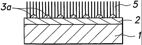
In step 1, an inorganic substrate 1 typically consisting of silicon or glass
is
cleansed (Figure 2a).
CA 02490074 2004-12-20
WO 2004/000728 PCT/JP2003/005628
-5-
In step 2, onto the inorganic substrate 1 is deposited an electroconductive
layer
2 consisting of a metal such as titanium (Ti), gold (Au), nickel (Ni), cobalt
(Co), copper
(Cu), aluminum (Al), molybdenum (Mo), tungsten (W), tantalum (Ta), or doped
semiconductor material, for instance, by vapor deposition using a resistive
heater or
sputtering (Figure 2b). When the inorganic substrate 1 consists of silicon, it
is preferable
to form an electroconductive layer 2 consisting of a two-layered structure
including a
titanium (Ti) layer formed over the substrate and a tungsten (W) layer formed
on the
titanium layer. Tungsten is preferred because it has a high melting point and
is therefore
resistant to the influences of the following thermal processes. Titanium
improves the
contact between the tungsten layer and substrate, and may be substituted by
nickel (Ni),
aluminum (Al) or chromium (Cr). Tungsten may be substituted by molybdenum (Mo)
or tantalum (Ta). If the inorganic substrate 1 consists of conductive silicon
(for instance,
doped silicon), it can be advantageously used for conducting electricity to an
external
circuit.
In step 3, a catalytic layer 3 consisting of a transition metal such as iron
(Fe)
and capable of a catalytic action for growing a carbon nanotube film is formed
on the
electroconductive layer 2 (Figure 2c). This can be accomplished by using
electron beam
vapor deposition. Iron may be substituted by nickel (Ni), cobalt (Co) or
molybdenum
(Mo). Alternatively, two or more members of a group consisting of iron,
nickel, cobalt
and molybdenum, or an alloy of such metals can also be used. This combination
of the
electroconductive layer 2 and catalytic layer 3 formed on the substrate 1 is
referred to as
an assembly 4 hereinafter.
Figure 3 is a schematic longitudinal sectional view of a preferred device for
forming a carbon nanotube on the electroconductive layer 2 by suitably
processing the
assembly 4 obtained in step 3. This device 10 comprises a quartz tube 12
defining an
CA 02490074 2004-12-20
WO 2004/000728 PCT/JP2003/005628
-6-
inner bore 30 mm in inner diameter for conducting desired gas along the length
thereof.
A quartz holder 14 is provided inside this tube 12 for holding the assembly 4
to be
processed. The quartz tube 12 is placed in an electric furnace 16 so as to be
heated to a
desired temperature.
Referring to Figure 1 once again, according to the present invention, in step
4,
the assembly 4 is secured to the quartz holder 14 in the quartz tube 12, and
is heated for
a prescribed period of time by suitably adjusting the temperature of the
electric furnace
16 while inert gas such as helium and argon is conducted through the quartz
tube 12
from an end (left end in Figure 3) thereof at a prescribed velocity. As a
result, the metal
or alloy of the catalytic layer 3 on the surface of the assembly 4 is turned
into fine
particles so that a large number of fine particles of the metal or alloy 3a
can be obtained
(Figure 2d). By thus processing the catalytic layer 3, and obtaining a large
number of
catalytic particles, the catalytic action during the process of growing the
carbon
nanotube can be enhanced. If the particles are not fine enough, the direction
of the
growth of the carbon nanotube may become uneven, and this prevents the
formation of
a clean film. A particle size below 50 nm is preferred. When forming fine
particles of
metal or alloy for the catalytic layer 3 by heating and supplying inert gas at
the same
time, the particles can be made finer as the heating temperature is increased.
However,
if the particle size is smaller than 0.5 nm, the aggregating force of the
particles becomes
so strong that the size of the particles in the aggregated parts thereof may
become even
greater, and it becomes difficult to control the particle size below 0.5 nm
and make the
particle size uniform at the same time. This leads to a reduction in
productivity.
Therefore, the particle size is preferred to be between 0.5 nm and 50 nm. The
process of
preparing the metallic or alloy particles for the catalytic layer 3 described
above will be
referred to as "preprocessing" hereinafter.
CA 02490074 2004-12-20
WO 2004/000728 PCT/JP2003/005628
-7-
The optimum heating temperature in the preprocessing may vary depending on
the kind of metal or alloy that is used in the catalytic layer 3. As will be
discussed in
connection with preferred embodiments, when the catalytic layer 3 is made of
iron (Fe),
the optimum heating temperature would be approximately 700 C (973 K). This
temperature in absolute (Kelvin) temperature is approximately 0.54 times the
melting
point of iron or 1808 K (1536 C), and is substantially equal to the
temperature from
which the atoms become able to move freely in solid (first recrystallization
temperature).
Thus, the optimum heating temperature for turning the metal or alloy for the
catalytic
layer into fine particles is in the vicinity of 0.54 Tm (0.54 Tm 0.05Tm)
where Tm is
the melting point of the metal or alloy in absolute temperature.
When the preprocessing is concluded, in step 5, the flow rate of the inert gas
is
reduced, and material gas (hydrocarbon gas) such as acetylene, methane and
ethylene is
introduced into the tube at a prescribed flow rate. This causes a carbon
nanotube having
a diameter in the range of 0.5 to 100 nm to grow on the electroconductive
layer 2, for
instance, in the form of a carbon nanotube film 5 having a thickness in the
range of 0.01
Rm to 300 m (Figure 2e). The produced carbon nanotube film 5 is generally
oriented
perpendicularly with respect to the assembly 4 or the substrate 1, and
demonstrates a
favorable electroconductivity in this direction. The material gas generates
hydrogen as
the carbon nanotube is produced, and the hydrogen along with the excess gas
(hydrocarbon) that was not used is expelled from the other end (right end in
Figure 3) of
the quartz tube 12.
During the process of forming the carbon nanotube, if the flow rate of the
material gas is excessive, amorphous carbon other than carbon nanotube or soot
is
produced, and this prevents the growth of the carbon nanotube resulting in a
reduction
of the content of the carbon nanotube in the film 5. Conversely, if the flow
rate of the
CA 02490074 2004-12-20
WO 2004/000728 PCT/JP2003/005628
-8-
material gas is inadequate, the growth of the carbon nanotube is reduced
resulting in a
poor productivity. The flow rate ratio of the material gas to the carrier gas
(inert gas) is
preferably from 1/2 to 1/50, and more preferably approximately 1/10.
The flow velocity of the mixed gas consisting of the inert gas and material
gas
along the surface of the assembly 4 also affects the formation of the carbon
nanotube
film 5. If the flow velocity is too small, soot is actively produced and the
content of the
carbon nanotube in the film 5 decreases. If the flow velocity is excessive,
much of the
material gas is expelled without contributing to the formation of the carbon
nanotube,
and the productivity is impaired. A flow rate in the range of 1 cm/minute to
100
cm/minute is preferred, and a flow rate in the range of 30 cm/minute to 40
cm/minute
(corresponding to approximately 200 to 300 sccm when the inner diameter of the
tube is
30 mm) is particularly preferred. A flow rate of approximately 30 cm/minute
(corresponding to approximately 200 sccm when the inner diameter of the tube
is 30
mm) is most preferred.
During the process of forming the film, by keeping the flow rate of the
material
gas and carrier gas (inert gas) constant, the carbon nanotube can be made to
grow
vertically with respect to the substrate. By slightly varying the flow rate,
the carbon
nanotube can be made to grow in a curved manner. Curving the carbon nanotube
promotes the entangling of the carbon nanotube fibers, and this in turn
increases the
firmness of the carbon nanotube film 5 and develops electroconductivity in
lateral
directions.
When the formation of the film is concluded, in step 6, the introduction of
the
material gas is terminated and the assembly is allowed to cool to the room
temperature
by continuing the flow of the inert gas. In step 7, the assembly 4 having the
carbon
nanotube film 5 formed thereon is removed from the electric furnace 16 and is
CA 02490074 2004-12-20
WO 2004/000728 PCT/JP2003/005628
-9-
processed by a high temperature in the atmosphere so that the amorphous carbon
and
the part of the carbon nanotube containing a large number of defects are
selectively
eliminated by oxidization and numerous gaps is produced in the carbon nanotube
film 5.
The part of the carbon nanotube having a substantially perfect crystalline
configuration
is resistant to oxidization and thereby remains unaffected. By suitably
controlling the
oxidization process, the density of the carbon nanotube fibers can be
adjusted. The
density of the carbon nanotube fibers may be in the order of 1,000 to 1012
fibers/mm2.
The agent for the oxidization may also consist of gas containing oxygen at a
prescribed
partial pressure or heated nitric acid as well as atmosphere.
Thus, according to the present invention, a large number of metallic or alloy
particles 3a can be formed by heating the metal or alloy in the catalytic
layer 2 formed
on the electroconductive member (electroconductive layer) 2 at a prescribed
temperature while supplying inert gas. The carbon nanotube film 5 can be
formed on the
electroconductive member 2 in a favorable manner by growing carbon nanotube
film 5
with the aid of the metallic or alloy particles 3a serving as a catalyst. For
the formation
of the carbon film, thermal CVD (which is also called as the chemical vapor
deposition
or chemical gas-phase growth method) was used in the foregoing embodiment, but
other
methods such as the microwave plasma method (plasma CVD), laser vapor
deposition
and sputtering can be also used.
When the carbon nanotube film 5 formed on the electroconductive member 2
as described above is used in a fuel cell, a catalyst such as platinum is
deposited on the
carbon nanotube film 5 and an electrolyte layer is placed thereon. Therefore,
when the
carbon nanotube film 5 is used in a fuel cell, the separator (inorganic
substrate 1),
electrode (electroconductive layer 2 and carbon nanotube film 5), platinum
catalyst and
electrolyte can be formed one over the other in a continuous matter and the
interfaces
CA 02490074 2004-12-20
WO 2004/000728 PCT/JP2003/005628
-10-
between these layers can be formed highly neatly. Therefore, as opposed to the
conventional fuel cell, there is no need to apply an external force to the
film/electrode
assembly (MEA) by using threaded bolts or the like for the purpose of reducing
the
contact resistance on the surface of the electrode, and the interface
resistance can be
minimized in a stable manner. Because the interface resistance can be
minimized both
easily and reliably, the production management can be simplified and the
productivity
can be improved. Also, the elimination of the threaded bolts or other means
for applying
an external force allows the size of the fuel cell to be minimized. Also,
using the carbon
nanotube film 5 in the fuel cell provides the following advantages. (1) The
overall
resistance of the fuel cell can be minimized because the carbon nanotube film
can be
formed as a thin film without any difficulty. (2) Because the hydrophobic
property that
is required for the oxygen electrode is produced on the surface of the carbon
nanotube
surface, the property of the fuel cell is prevented from being prematurely
degraded by
the clogging of the pores with water. (3) Because the carbon nanotube having a
relatively high crystalline configuration is resistant to corrosion, the
service life of the
fuel cell can be extended. (4) Because the carbon nanotube is highly porous,
it serves as
an excellent gas diffusion layer which favorably permits transmission of gas
such as
hydrogen and oxygen and offers a large surface area for adequately promoting
the
reaction.
With reference to the schematic sectional view of Figure 4, another
embodiment of the method for forming a carbon nanotube according to the
present
invention is described in the following. The device illustrated in Figure 3
was used for
the film forming process.
A silicon substrate 21 having a mirror finished surface is cleansed in
sulfuric
acid - hydrogen peroxide for 10 minutes, and is then rinsed in water. Oxide
film thereon
CA 02490074 2004-12-20
WO 2004/000728 PCT/JP2003/005628
-11-
is removed by using buffered hydrofluoric acid (MHF) and is dried (Figure 4a).
Titanium (Ti) film 22a is formed on the cleansed silicon substrate 21 to a
thickness of
50 nm at the rate of 1 nm/sec under a pressure of 6 x 10⁻⁵ Pa by resistive
heating vapor
deposition, and tungsten (W) film 22b is formed thereon to a thickness of 100
nm under
an Ar partial pressure of 5 x 10⁻³ Torr (6.7 x 10⁻⁴ Pa) by RF sputtering
(Figure 4b). The
RF sputtering is suited for forming film of material having a high melting
point such as
tungsten. The titanium (Ti) film 22a and tungsten (W) film 22b forms an
electroconductive layer 22. Then, under a pressure of 1 x 10⁻⁴ Pa, iron (Fe)
is deposited
on the tungsten film 22b at the rate of 0.1 nm/sec to a thickness of 5 nm so
as to form a
catalytic layer 23 having a thickness of 5 nm (Figure 4c). Electron beam vapor
deposition is suited for forming film of material having a relatively low
melting point
such as iron. The assembly having the electroconductive layer 22 and catalytic
layer 23
formed on the silicon substrate 21 is secured to the quartz holder 14 placed
in the quartz
tube 12 in the thermal CVD device 10 shown in Figure 3. The inner diameter of
the
quartz tube 12 is 30 mm. Helium gas is introduced into the quartz tube 12 at
the flow
rate of 230 sccm, and the temperature of the electric furnace 16 is set to
approximately
700 C. When the temperature of the electric furnace 16 substantially reaches
700 C,
the same temperature is maintained for 5 to 30 minutes so that the iron 23 on
the surface
of the assembly turns into fine particles 23a (Figure 4d).
Figure 5 includes photographs that show the state of the iron particles 23a
when the heating temperature was changed. As shown in Figure 5(a), when the
heating
temperature was 600 C which is lower than 700 C, the iron did not adequately
turn
into fine particles. As shown in Figure 5(c), when the heating temperature was
800 C
which is higher than 700 C, the iron particles became coarse and failed to
turn into
adequately fine particles. According to the present embodiment, the iron on
the surface
CA 02490074 2004-12-20
WO 2004/000728 PCT/JP2003/005628
-12-
turned into fine particles in an optimum fashion when the heating temperature
was 700
C. Thus, according to the present invention, the heating temperature of 700 C
was
most desirable in obtaining fine particles for the catalytic layer 23.
However, how the
catalytic metal turns into fine particles very much depends on the thickness
of the
catalytic layer 23, wettability of the lower electroconductive layer 22,
configuration of
the electroconductive layer 22 and heating time, and the optimum temperature
may well
depend on such factors.
After the iron of the catalytic layer 23 turns into small particles, acetylene
(C2H2) is introduced into the tube at the flow rate of 30 sccm while the flow
rate of
helium is reduced to 200 sccm. After about fifteen minutes of processing, a
multi-walled nanotube (MWNT) 25 having a thickness of approximately 30 m is
obtained (Figure 4e). Thereafter, the supply of acetylene is tenninated and
the assembly
is cooled to the room temperature by flowing helium. The assembly 24 having
the
MWNT 25 formed thereon is removed from the tube, and amorphous carbon is
removed
by processing the assembly in the atmosphere for five minutes at the
temperature of 700
C. This produces a carbon nanotube structure having numerous gaps therein. The
produced carbon nanotube consists of MWNT having a diameter in the range of 10
to
50 nm and the film is formed by fibers extending perpendicularly to the
substrate.
Thus, according to the present invention, the metal or alloy of the catalytic
layer can be turned into fine particles both easily and reliably by first
forming the
catalytic layer consisting of the metal or alloy serving as a catalyst for
forming a carbon
nanotube on an electroconductive member and then keeping it at a prescribed
temperature while supplying inert gas, and the catalytic particles prepared in
this
manner allow the carbon nanotube to be formed on the electroconductive member
in an
efficient manner.
CA 02490074 2004-12-20
WO 2004/000728 PCT/JP2003/005628
-13-
Although the present invention has been described in terms of preferred
embodiments thereof, it is obvious to a person skilled in the art that various
alterations
and modifications are possible without departing from the scope of the present
invention which is set forth in the appended claims.