Note: Descriptions are shown in the official language in which they were submitted.
CA 02490096 2010-06-01
= 52867-11
High Speed, High Density Interconnection Device
TECHNICAL FIELD
This description relates to interconnection devices, and more
particularly to interconnection devices which connect an array of contacts
within a
digital or analog transmission system.
BACKGROUND
High speed communication between two printed circuit cards over
an interconnection device with a dense array of contacts may result in cross-
talk
between communication channels within the interconnection device and a
resulting degradation of signal integrity. In addition to cross-talk between
communication channels, high speed communication across an interconnection
device may generate undesirable levels of noise. Reduction of cross-talk and
noise while at the same time maintaining a dense array of contacts within an
interconnection device is often a design goal.
SUMMARY
According to one aspect of the present invention, there is provided
an intercoupling component for receiving an array of contacts within a digital
or
analog transmission system having an electrical ground circuit and a chassis
ground circuit, the intercoupling component comprising: a segment formed of
electrically insulative material and having an upper and lower surface, the
segment including a plurality of holes disposed on its upper surface and
arranged
in a predetermined footprint corresponding to the array of a contacts; a
shield
member formed of electrically conductive material and at least partially
disposed
within the segment and configured to electrically connect to the chassis
ground
circuit; a plurality of electrically conductive signal contacts configured to
transmit a
digital or analog communication signal, each signal contact disposed within a
hole
on the upper surface of the segment forming an array of signal contacts, and
wherein the shield member is at least partially disposed within the array of
signal
I
CA 02490096 2010-06-01
52867-11
contacts; and a frame formed of electrically conductive material at least
partially
surrounding the segment and in electrical contact with the shield member and
configured to electrically connect to the chassis ground circuit.
According to another aspect of the present invention, there is
provided an intercoupling component for receiving an array of contacts within
a
digital or analog transmission system having an electrical ground circuit and
a
chassis ground circuit, the intercoupling component comprising: a plurality of
segments formed of electrically insulative material, spaces between adjacent
segments defining at least one gap, each segment having an upper and lower
surface and including a plurality of holes disposed on its upper surface and
arranged in a predetermined footprint corresponding to the array of a
contacts; a
shield member formed of electrically conductive material disposed within at
least
one gap between adjacent segments and configured to electrically connect with
the chassis ground circuit of the system; a plurality of shield members formed
of
electrically conductive material disposed within a plurality of gaps between
adjacent segments configured to electrically connect with the chassis ground
circuit of the system; and a frame formed of electrically conductive material
surrounding the plurality of segments and in electrical contact with the
plurality of
shield members.
According to another aspect of the present invention, there is
provided an intercoupling component for receiving an array of contacts within
a
digital or analog transmission system having an electrical ground circuit and
a
chassis ground circuit, the intercoupling component comprising: a segment
formed
of electrically insulative material and having an upper and lower surface, the
segment including a plurality of holes disposed on its upper surface and
arranged
in a predetermined footprint corresponding to the array of a contacts; a
plurality of
electrically conductive contacts each disposed within each hole on the upper
surface of the segment, wherein the plurality of contacts are arranged in a
plurality
of multi-contact groupings, at least one multi-contact grouping comprising: a
first
electrically conductive contact; and a reference contact located at a distance
D from the first electrically conductive contact and configured to
electrically
1a
CA 02490096 2010-06-01
52867-11
connect to the electrical ground circuit of the system, wherein the first
electrically
conductive contact and the reference contact form a transmission line
electrically
equivalent to a co-axial transmission line.
According to another aspect of the present invention, there is
provided an intercoupling component for receiving an array of contacts within
a
digital or analog transmission system having an electrical ground circuit and
a
chassis ground circuit, the intercoupling component comprising: a segment
formed
of electrically insulative material and having an upper and lower surface, the
segment including a plurality of holes disposed on its upper surface and
arranged
in a predetermined footprint corresponding to the array of a contacts; and a
plurality of electrically conductive contacts each disposed within each hole
on the
upper surface of the segment, wherein the plurality of contacts are arranged
in a
plurality of multi-contact groupings, at least one multi-contact grouping
comprising:
a first electrically conductive contact; and a reference contact located at a
distance
D from the first electrically conductive contact and configured to
electrically
connect to the electrical ground circuit of the system, and wherein the first
electrically conductive contact is configured to transmit single-ended
signals.
According to another aspect of the present invention, there is
provided an intercoupling component for receiving an array of contacts within
a
digital or analog transmission system having an electrical ground circuit and
a
chassis ground circuit, the intercoupling component comprising: a segment
formed
of electrically insulative material and having an upper and lower surface, the
segment including a plurality of holes disposed on its upper surface and
arranged
in a predetermined footprint corresponding to the array of a contacts; and a
plurality of electrically conductive contacts each disposed within each hole
on the
upper surface of the segment, wherein the plurality of contacts are arranged
in a
plurality of multi-contact groupings, at least one multi-contact grouping
comprising:
a first electrically conductive contact; a second electrically conductive
contact
member located at a distance D from the first electrically conductive contact;
and
a reference contact located at a distance D2 from the first electrically
conductive
lb
CA 02490096 2010-06-01
52867-11
contact and configured to electrically connect to the electrical ground
circuit of the
system.
According to another aspect of the present invention, there is
provided a circuit card for use in a digital or analog transmission system
having an
electrical ground circuit and a chassis ground circuit, the circuit card
comprising: a
printed circuit board having a plurality of contact pads arranged in a
predetermined footprint; and an interconnection device comprising: a segment
having an upper and lower surface, the segment having a plurality of holes
extending through the upper and lower surfaces and arranged in a predetermined
footprint to match the predetermined footprint of the plurality of surface
mount
pads; a plurality of electrically conductive contact member disposed within
each of
the holes and electrically connected to their respective surface mount pad; a
shield member formed of electrically conductive material disposed within the
segment; and a frame formed of electrically conductive material surrounding
the
segment, the frame electrically connected to the shield member and to the
chassis
ground circuit of the system.
According to another aspect of the present invention, there is
provided an intercoupling component for receiving an array of contacts within
a
digital or analog transmission system having an electrical ground circuit, the
intercoupling component comprising: a segment formed of a material having a
dielectric constant Er1, and having an upper and lower surface, the segment
including a plurality of holes disposed on its upper surface and arranged in a
predetermined footprint corresponding to the array of a contacts; a first
signal
contact disposed within a first hole on the segment; a second signal contact
disposed within a second hole on the segment adjacent to the first hole in
which
the first signal contact is disposed, and wherein a cavity is formed in the
segment
between the first and second hole; and an insert formed of a material having a
dielectric constant of Er2, the insert disposed within the cavity.
According to another aspect of the present invention, there is
provided a method for adjusting the differential impedance of a pair of
differential
transmission lines in an interconnection device for receiving an array of
contacts
1c
CA 02490096 2010-06-01
52867-11
within a digital or analog transmission system having an electrical ground
circuit,
the intercoupling component comprising, the method comprising: providing a
segment formed of a material having a dielectric constant Er1 and having an
upper and lower surface, the segment including a plurality of holes disposed
on its
upper surface; providing a plurality of pairs of signal contacts, each pair
disposed
with two adjacent holes on the segment and configured to transmit differential
signals, the plurality of pairs of signal contacts forming an array of pairs
of signal
contacts disposed in the segment; spacing the pairs of signal contacts such
that
they create a certain differential impedance between the two contacts in each
pair
of signal contacts; and providing a plurality of cavities disposed in the
segment
between the two signal contacts in each pair of signal contacts to adjust the
differential impedance of the two signal contacts in each pair of signal
contacts.
In an aspect, the invention features an intercoupling component for
receiving an array of contacts within a digital or analog transmission system
having an electrical ground circuit and a chassis ground circuit. A plurality
of
electrically conductive contacts are disposed within holes formed on a segment
formed of insulative material. One or more electrically conductive shields are
disposed within the segment and are configured to connect to the chassis
ground
circuit of the system.
Embodiments may include one or more of the following. At least
some of the plurality of the electrically conductive contacts disposed within
the
holes on the segment may be configured to electrically connect with the
electrical
ground circuit of the system.
A frame formed of electrically conductive material may surround the
segment and be in electrical contact with both the shield member and the
electrical ground circuit of the system. The frame may be molded around the
segments.
1d
CA 02490096 2004-12-20
WO 2004/001912 PCT/US2003/019830
One or more ground planes which are configured to electrically connect with
the
electrical ground circuit of the system may be disposed within the segment.
One or more
cavities filled with air may be disposed on the segment.
The intercoupling component may further include a retention member configured
to releasably retain an array mating of contacts with the plurality of
electrically
lo conductive contacts.
In another aspect, the invention features an intercoupling component for
receiving
an array of contacts within a digital or analog transmission system having an
electrical
ground circuit and a chassis ground circuit. A plurality of electrically
conductive
contacts are disposed within holes formed on a plurality of segments, each
formed of
insulative material. One or more electrically conductive shields are disposed
within gaps
between adjacent segments and are connected to the chassis ground circuit of
the system.
In another aspect, the invention features an intercoupling component for
receiving
an array of contacts within a digital or analog transmission system having one
or more
segments formed of electrically insulative material and having an upper and
lower
surface, the segment including a plurality of holes disposed on its upper
surface and
arranged in a predetermined footprint corresponding to the array of a contacts
and a
plurality of electrically conductive contacts each disposed within each hole
on the upper
surface of the segment. The plurality of contacts are arranged in a plurality
of multi-
contact groupings, with at least one multi-contact grouping including a first
electrically
conductive contact and a reference contact. The reference contact is located
at a distance
D from the first electrically conductive contact and is configured to
electrically connect
to the electrical ground circuit of the system.
Embodiments may include one or more of the following. The first electrically
conductive contact and reference may be configured to form a transmission line
electrically equivalent to a co-axial transmission line. The first
electrically conductive
contact may be configured to transmit single-ended signals. Additionally, each
multi-
contact grouping may be located a distance of >D from adjacent multi-contact
groupings.
2
CA 02490096 2004-12-20
WO 2004/001912 PCT/US2003/019830
The intercoupling component may also include a second electrically conductive
contact member located at a-distance D2 from the first electrically conductive
contact.
The first and second electrically conductive contacts may form a transmission
line
electrically equivalent to a twin-axial differential transmission line. The
first and second
electrically conductive contacts within each multi-contact grouping may be
configured to
transmit disparate single-ended signals or low-voltage differential signals.
Additionally,
each multi-contact grouping may be located a distance > D2 from adjacent multi-
contact
groupings.
The first and second electrically conductive contacts may have substantially
the
same cross-section, initial characteristic impedance, capacitance, and
inductance.
The intercoupling component may also include one or more shield members
formed of electrically conductive material disposed within the segment and
configured to
connect to the chassis ground circuit of the system. Additionally, the
intercoupling
component may include a frame disposed around the one or more segments.
In another aspect of the invention, a circuit card for use in a digital or
analog
transmission system having an electrical ground circuit and a chassis ground
circuit, the
circuit card includes a printed circuit board having a plurality of contact
pads arranged in
a predetermined footprint; and an interconnection device. The interconnection
device
includes one or more segments having an upper and lower surface, the upper
surface of
the segment having a plurality of holes arranged in a predetermined footprint
to match the
predetermined footprint of the plurality of surface mount pads, a plurality of
electrically
conductive contact member disposed within each of the holes and electrically
connected
to their respective surface mount pad, and one or more a shield members formed
of
electrically conductive material disposed within the segment. Additionally, a
frame
formed of electrically conductive material surrounds the one or more segments
and the
frame is electrically connected the shield member and to the chassis ground
circuit of the
system.
Additional embodiments include one or more of the following features. The
plurality of contacts may be arranged in a plurality of multi-contact
groupings which
3
CA 02490096 2004-12-20
WO 2004/001912 PCT/US2003/019830
includes a first electrically conductive contact; and a reference contact
located at a
distance D from the first electrically conductive contact and connected to the
electrical
ground circuit of the system.
The plurality of multi-contact groupings may also include a second
electrically
conductive contact located a distance D2 from the first electrically
conductive contact.
The first and second electrically conductive contacts have substantially the
same
cross-section, capacitance and inductance. The first and second electrically
conductive
contacts may be configured to transmit low voltage differential signals or
disparate single
ended signals.
In another aspect of the invention, an intercoupling component for receiving
an
array of contacts within a digital or analog transmission system having an
electrical
ground circuit, the intercoupling component includes a. segment formed of a
material
having a dielectric constant Erl. The segment has an upper and lower surface
and a
plurality of holes are disposed on the upper surface of the segment. A first
signal contact
disposed within a first hole on the segment and a second signal contact
disposed within a
second hole on the segment adjacent to the first hole in which the first
signal contact is
disposed. The segment also includes a cavity formed between the first and
second signal
contacts.
Additional embodiments include one or more of the following features. The
cavity may be formed on the upper surface, lower surface or within the segment
and may
be is open to air. An insert formed of a material having a dielectric constant
of Erg may
be disposed within the cavity.
The intercoupling component may include a plurality of first signal contacts
disposed within a plurality of holes and a plurality of second signal contacts
each
disposed within a hole that is adjacent to a hole containing a first signal
contact. The
segment may include a cavity disposed between each pair of first and second
signal
contacts. The intercoupling component may also include ground contacts
disposed
within holes on the segment or a ground plane.
4
CA 02490096 2004-12-20
WO 2004/001912 PCT/US2003/019830
In another aspect of the invention, a method for adjusting the differential
impedance of a pair of differential transmission lines in a interconnection
device for
receiving an array of contacts within a digital or analog transmission system
having an
electrical ground circuit, the intercoupling component. The method includes
providing a
segment having a dielectric constant Erl and having an upper and lower surface
and
including a plurality of holes disposed on its upper surface. Providing a pair
of signal
contacts disposed within two adjacent holes on the segment, the pair of signal
contacts
configured to transmit differential signals. Spacing the pair of signal
contacts such that
they create a certain differential impedance of the two contacts in the pair
of signal
contacts. Providing a cavity in the segment between the two signal contacts in
the pair of
signal contacts to adjust the differential impedance between the pair of
signal contacts.
Additional embodiments include one or more of the following steps. Inserting a
material having a dielectric constant of Erg in the cavity in the segment.
Providing a plurality of pairs of signal contacts disposed with a plurality of
adjacent holes on the segment, the plurality of pairs of signal contacts
forming an array of
pairs of signal contacts disposed in the segment. Providing a plurality of
cavities
disposed in the segment between the two signal contacts in each pair of signal
contacts to
adjust the differential impedance of the two signal contacts in each pair of
signal
contacts.
Providing a plurality of ground contacts disposed within a plurality of holes
on
the segment and within the array of pairs of signal contacts, the plurality of
ground
contacts electrically connected to the electrical ground circuit of the
system.
Providing a ground plane disposed within the segment and within the array of
pairs of signal contacts, the ground plane configured to electrically connect
with the
electrical ground of the system.
Embodiments of the invention may have one or more of the following advantages.
One or more contacts disposed within the array of contacts and are configured
to
connect to the electrical ground of the system may help to reduce cross-talk
between two
or more contacts during signal transmission. Additionally, the use of a
electrically
5
CA 02490096 2004-12-20
WO 2004/001912 PCT/US2003/019830
conductive shield member connected to the chassis ground of the system and
disposed
within or between one or more segments may help to reduce undesired
electromagnetic
fields generated by high-speed electron flow over the contact array during
operation.
The details of one or more embodiments of the invention are set forth in the
accompanying drawings and the description below. Other features, objects, and
lo advantages of the invention will be apparent from the description and
drawings, and from
the claims.
DESCRIPTION OF DRAWINGS
FIG 1 is a is a perspective view, partially exploded, of an plug on a
secondary
circuit board and a matching socket on a primary circuit board within an
digital or analog
signal transmission system.
FIG 2A is a perspective view of a plug.
FIG 2B is a side view of a plug, partially cut away.
FIG 3A is a perspective view of a plug shield.
FIG 3B is a perspective view of a plug segment.
FIG 3C is a bottom view of a plug.
FIG 4A is a perspective view of a socket, partially exploded.
FIG 4B is a side view of a socket, partially cut away, partially exploded.
FIG 5A is a perspective view of socket shield.
FIG 5B is a perspective view of a socket segment.
FIG 5C is a bottom view of a socket.
FIG 6 is a schematic of an interconnection device in operation.
FIG 7 is a partial view of three contact groupings within a socket.
FIG 8 is a partial view of three contact groupings within a socket and air
cavities
disposed on the socket.
FIG. 9 is a partial view of three contact groupings and a continuous ground
plane
disposed within another interconnection device.
FIG 10 is a partial view of three contact groupings and a number of ground
planes
disposed within another interconnection device.
6
CA 02490096 2004-12-20
WO 2004/001912 PCT/US2003/019830
FIG 11 is a partial view of three contact groupings and a number of ground
planes
disposed within another interconnection device.
DETAILED DESCRIPTION
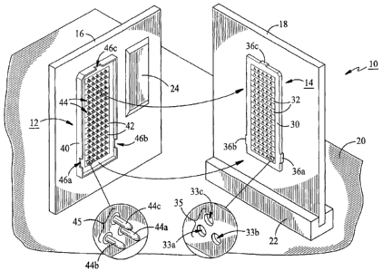
Referring to FIG 1, in a digital or analog signal transmission system 10, a
plug 12
and matching socket 14 releasably connect two printed circuit boards, a
primary circuit
board 18 and a secondary circuit board 16.
Digital or analog transmission system 10 may be any system which transmits
digital or analog signals over one or more transmission lines, such as a
computer system
(as illustrated in FIG 1), a telephony switch, a multiplexor / demultiplexor
(MUX/DMUX), or a LAN/WAN cross-connect/router.
Secondary circuit board 16 may include a central processing unit (CPU),
application specific integrated circuit (ASIC), memory, or similar active or
passive
devices and components. In this example, secondary circuit board 16 includes
an ASIC
device 24, and primary circuit board 18 is a daughter board connected to a
motherboard
by a card slot connector 22. In another embodiment, the primary circuit board
may be
20 a self-contained system or board, not connecting to any other system or
motherboard, as
in the case of a single board computer.
The socket 14 includes a frame 30 formed of electrically conductive material
that
surrounds a number of segments 32. The segments 32 are formed of electrically
insulative material. A shield (not shown in FIG 1) formed of electrically
conductive
material is located between each of the segments 32 and is in electrical
contact with the
frame 30, thus forming an electrically conductive "cage" around the perimeter
of each
segment 32. As will be explained in greater detail below, the frame 30 is
electrically
connected to the chassis ground circuit (shown in FIG 6) of the system 10.
The socket 14 has an array of holes arranged in a series of three-hole
groupings
35 on each segment 32. A female socket assembly 34 (not shown in FIG 1) is
located
within each of the holes 33a-33c and is configured to releasably receive a
male pin. As
will be explained in greater detail below, the three-contact grouping 35
includes a first
signal contact (disposed within hole 33a), a second signal contact (disposed
within hole
7
CA 02490096 2004-12-20
WO 2004/001912 PCT/US2003/019830
33b) and a reference contact (disposed within hole 33c). The reference contact
is
electrically connected to the electrical ground circuit (Vcc) (shown in FIG 6)
of the
system 10.
Plug 12, which mates with socket 14, also includes a frame 40 formed of
electrically conductive material that surrounds a number of segments 42. Like
the socket
segments 32, the plug segments 42 are formed of electrically insulative
material. A shield
(not shown in FIG. 1) formed of electrically conductive material is located
between each
of the segments 42 and is in electrical contact with the frame 40, thus
forming an
electrically conductive "cage" around the perimeter of each segment 42 within
the plug
12. As will be explained more below, the frame 40 is electrically connected to
the chassis
ground circuit (shown in FIG 6) of the system 10.
The plug 12 has an array of male pins 44 arranged in a series of three-pin
groupings 45 on each segment 42. Each three-pin grouping 45 includes a first
signal pin
44a, a second signal pin 44b and a reference pin 44c. As will be explained in
greater
detail below, these three pins mate with their respective sockets to form a
twin-axial
communication channel and a reference ground return between the plug 12 and
socket 14.
Each of the male pins 44 protrude from the upper surface of the segments 42
and
are received by the matching array of female sockets (not shown) disposed
within each of
the holes 34 on the socket 14. Each male pin and female socket attach to a
solder ball
(not shown in FIG 1) that protrudes from the bottom surface of the plug 12 and
socket
14, respectively, and is mounted via a solder reflow process to contact pads
on the
respective printed circuit boards, 16, 18. Thus, when the plug 12 is inserted
into the
socket 14, an electrical connection is formed between the secondary circuit
board 16 and
primary circuit board 18. In separate embodiments, the male pins 44 and female
sockets
34 may not be terminated by a solder reflow process using solder balls, but
may employ
other methods for mounting the pins or sockets to a printed circuit card, such
as through-
hole soldering, surface mount soldering, through-hole compliant pin, or
surface pad
pressure mounting.
8
CA 02490096 2004-12-20
WO 2004/001912 PCT/US2003/019830
The plug frame 40 includes three guide notches 46a, 46b, 46c which mate with
the three guide tabs 36a, 36b, 36c on the socket frame 30 in order to ensure
proper
orientation of the plug 12 and the socket 14 when mated together.
Referring to FIGS. 2A-B, each male pin 44 extends from the lower surface of
the
plug 12 and protrudes from the upper surface of the segments 42. A solder ball
50 is
1o attached (e.g., by soldering) to the terminal end of each male pin 44 and
protrudes from
the bottom surface of the plug. The array of solder balls 50 attached to the
terminal end
of each male pin 44 may be mounted (e.g., by a solder reflow process) to
contact pads
located on the secondary circuit board 16.
The plug frame 40 is formed of electrically conductive material and includes
solder balls 52 are attached (e.g., by a solder reflow process) to the bottom
surface of the
plug frame 40. When the plug 14 is mounted to the secondary circuit board 16,
the solder
balls 52 attached to the plug frame 40 are electrically connected to the
chassis ground
circuit of the system 10.
Referring to FIGS. 3A-C, a shield (FIG 3A), a segment (FIG 3B) and the bottom
surface of the plug (FIG 3C) is shown. A shield 60 formed of electrically
conductive
material is located between each of the segments 42. Each shield 60 is
generally U-
shaped and includes two short sides 61, 62 on each side of a longer middle
portion 63.
When assembled into the plug, the two short sides 61, 62 of each shield 60 are
in
electrical contact with the frame 40, while the middle portion 63 of each
shield 60 is
located between each of the segments 42. Thus, the frame 40 and shields 60
form a
electrically conductive "cage" around the perimeter of each segment 42. This
electrically
conductive "cage" is connected to the chassis ground circuit (shown in FIG 6)
of the
system 10 via solder balls 52 on the bottom of the frame 40. The chassis
ground circuit is
a circuit within system 10 which connects to the metal structure on or in
which the
components of the system are mounted.
In this example, each shield 60 has four notches: two on the short sides of
the
shield 64, 65 and two on the middle portion of the shield 66, 67. When the
shields 60 are
assembled into the plug 12, the two notches on the short sides of each shield
64, 65 mate
9
CA 02490096 2004-12-20
WO 2004/001912 PCT/US2003/019830
with the two dog-eared tabs 71, 72 on each corresponding segment 42.
Similarly, the two
notches located on the middle portion 66, 67 of each shield 60 mate with two
corresponding tabs (not shown) on each segment 42. Each shield 60 also has
three tabs
68 on it's middle portion 63 which are pressed in opposite directions by
adjacent
segments 42 after the plug 12 assembled and helps to secure the shields 60 in
place.
Each segment 42 includes two dog-eared tabs 71, 72 located at each end of the
segment 42. The two dog-eared tabs 71, 72 fit into two matching grooves 81, 82
formed
on the bottom surface of the frame 40. The two triangular bump-outs 73, 74 on
each of
the segments 42 press against adjacent shields 60 and segments 42 in order to
secure the
segments 42 and the shields 60 within the frame 40. It should be noted that
there are
many ways to secure the segments 42 and shields within the frame 40 such as by
glue,
adhesive, cement, screws, clips, bolts, lamination or the like. The frame 40
may also be
constructed by partially encapsulating the segments 42 with an electrically
conductive
resin or other material.
Referring to FIGS. 4A-B, the socket 14 has an array of holes (e.g., 33a, 33b,
33c)
disposed on the segments 32. A female socket contact 34 is disposed within
each of the
holes and is configured to releasably receive a corresponding male pin 44. A
solder ball
contact 90 is attached (e.g., by soldering) to the terminal end of each female
socket
contact 34 and protrudes from the bottom surface of the socket 12. The array
of solder
balls 90 attached to the terminal end of each female socket contact 34 may be
mounted
(e.g., by soldering) to contact pads located on the primary circuit board 18.
Like the plug frame 40, the socket frame 30 is formed of electrically
conductive
material and includes solder balls 92 attached (e.g., by soldering) to the
bottom surface of
the socket frame 30. When the socket 14 is mounted to the primary circuit
board 18, the
solder ball contacts 92 attached to the socket frame 30 are electrically
connected to
contact pads which are connected to the chassis ground circuit of the system
10.
Additionally, when the plug 12 is inserted into the socket 14, the plug frame
40 and
socket frame 30 are electrically connected to each other and are, in turn,
electrically
connected to the chassis ground circuit of the system 10.
CA 02490096 2004-12-20
WO 2004/001912 PCT/US2003/019830
As shown in FIGS. 5A-C, the assembly of the socket 14 is similar to the
assembly
of the plug 12 depicted in FIGS. 3A-C. Dog-eared tabs 102, 103 located on the
socket
segments 32 fit into corresponding notches 104, 105 disposed on the socket
frame 30. A
shield 100 is located between each of the segments and electrically contacts
the socket
frame 30, thus forming an electrically conductive "cage" around the perimeter
of each
socket segment 32.
The male pins 44 on the plug 12 and corresponding female socket contacts 34
disposed within the socket 14 may be any mating pair of interconnection
contacts and not
restricted to pin-and-socket technology. For example, other embodiments may
use fork
and blade, beam-on-beam, beam-on-pad, or pad-on-pad interconnection contacts.
As will
be explained in greater detail below, the choice of contact may effect the
differential
impedance of the signal channels.
Referring to FIG 6, in digital or analog signal transmission system 10,
differential
signal communication over a single three-contact grouping between secondary
circuit
board 16 and primary circuit board 18 is illustrated. The plug 12 mounted to
the
secondary circuit board 16 is plugged into the socket 14 mounted to the
primary circuit
board 18, forming an electrical connection between the primary and secondary
circuit
boards, 16, 18. Within the three-contact grouping, three male pins (not shown
in FIG 6)
of the plug 12 and three corresponding female socket contacts of socket 14
couple to
form a first signal channel 108, a second signal channel 110, and a reference
channel 112.
The first and second signal channels 108, 110 are coupled with a resistor 118
to form a
symmetric differential pair transmission line. The reference channel 112 is
electrically
connected to the electrical ground circuit (Vcc) 114 of the system 10. The
electrical
ground circuit (Vcc) 114 is a circuit within system 10 that is electrically
connected to the
power supply (not shown) of system 10 and provides the reference ground for
system 10.
3o Additionally, the plug frame 40 and socket frame 50 are in electrical
contact with each
another and with the chassis ground circuit 120 of the system 10.
In this example, an ASIC chip 24 mounted to the secondary circuit board 18
includes a driver 100 which sends signals over the first and second signal
channels, 108,
11
CA 02490096 2004-12-20
WO 2004/001912 PCT/US2003/019830
110. The primary circuit board 18 includes a receiver 116 which receives the
signals
generated by the driver 100. The receiver 116 may be incorporated within a
memory
device, a central processing unit (CPU), an ASIC, or another active or passive
device.
The receiver 116 includes a resistor 118 between the first signal channel 108
and the
second signal channel 110. In order to avoid signal reflection due to
mismatched
lo impedance, the differential impedance of the first and second signal
channels, 108, 110
should be such that it approximately matches the value of the resistor 118.
The driver 100 includes a current source 102 and four driver gates 104a-104b,
106a-106b and drives the differential pair line (i.e., first and second signal
channels. 108,
110). The receiver 116 has a high DC input impedance, so the majority of
driver 100
current flows across the resistor 118, generating a voltage across the
receiver 116 inputs.
When driver gates 106a-106b are closed (i.e., able to conduct current) and
driver gates
104a-104b are open (i.e., not able to conduct current), a positive voltage is
generated
across the receiver 116 inputs which may be associated with a valid "one"
logic state.
When the driver switches and driver gates 104a-104b are closed and driver
gates 106a-
106b are open, a negative voltage is generated across the receiver inputs
which may be
associated with a valid "zero" logic state.
The use of differential signaling creates two balanced signals propagating in
opposite directions over the first and second signal channels, 108, 110. The
electromagnetic field generated by current flow of the signal propagating over
the first
signal channel 108 is partially cancelled by the electromagnetic field
generated by the
current flow of the signal propagating over the second signal channel 110 once
the
differential signals become co-incidental or "in-line" with one another. Thus,
the
differential signaling reduces cross-talk between the first and second signal
channels and
between adjacent contact groupings.
The addition of the reference channel 112 in close proximity to the first and
second channels 108, 110 functions to help bleed off the parasitic
electromagnetic field to
circuit ground 114, which may further reduce cross-talk between signal
channels and
between contact groupings.
12
CA 02490096 2004-12-20
WO 2004/001912 PCT/US2003/019830
The driver 100 may also be configured to operate in an "even" mode where two
signals propagate across the first and second channel at the same time in the
same
direction. In this mode, current travels in the same direction over the first
and second
signal channels, 108 and 110, and, therefore the electromagnetic fields
generated by the
current flow would largely add. However, the reference channel 112 would still
operate
to bleed off the electromagnetic field and reduce cross-talk between adjacent
contacts and
contact groupings.
The socket 12 and plug 14 also feature electrically conductive "cages" formed
by
the frame and the shields around the perimeter of the segments, 34, 44. The
plug frame
40 and socket frame 30 are in electrical contact with each other and with the
chassis
ground 120 of the system 10. When high speed communication takes place over an
interconnection device, electromagnetic fields substantially parallel to the
board are
created due to the electron flow at high frequencies. The frames 30, 40 and
the shields
32, 42, act as "cages" to contain the electromagnetic fields generated by the
electron flow
across the device, which may reduce the amount of noise emitted by the
interconnection
device. Additionally, the "cages" act to absorb electromagnetic fields which
might
otherwise be introduced into the socket 12 and plug 14, and which may
adversely affect
the primary or secondary circuit boards 18, 16 and any associated active or
passive
devices and components mounted thereto.
Referring again to FIG. 6, when a pair of interconnection devices are mated,
the
differential impedance for the first and second signal channels should be
approximately
equal to the value of resistor 118 in order to avoid reflection of the signal.
In a Low
Voltage Differential Signaling (LVDS) application, the value of the resistor
118 is
typically 100 ohms. Thus, in a pair of interconnection devices for use in an
LVDS
application, the first and second signal channels should be designed such the
differential
impedance is approximately 100 ohms. The differential impedance of the first
and
second channel signal is a complex calculation that will depend on a number of
variables
including the characteristic impedance of the contacts, the dielectric
constant of the
medium surrounding the contacts, and the spatial orientation of the signal
contacts and
13
CA 02490096 2004-12-20
WO 2004/001912 PCT/US2003/019830
the reference ground contacts. One simplified analytical approach to
determining the
differential impedance, might be as follows:
(1) First determine the self inductance and self capacitance for each of the
signal
channels with respect to the reference channel within a unit given a selected
conductor
cross section and spatial relationship.
(2) Determine the differential mutual inductance and capacitance between the
two signal channels within a unit given the selected conductor cross section
and spatial
relationship; and
(3) Combine the self impedance (i.e., the self inductance plus self
capacitance)
and differential mutual impedance (i.e., the differential mutual inductance
plus
differential mutual capacitance) to approximate the differential impedance of
the two
signal channels.
A similar analytical approach may be used to orient the units with respect to
one
another. It should be noted, however, that these analytical approaches are
idealized and
does not account for parasitics produced in real-world transmission lines. Due
to the
complexity of the calculations for real-world transmission lines, computer
modeling and
simulations using different parameters is often an efficient way to arrange
the contacts for
a particular application.
Referring to FIG. 7, the spacing between the three groups of three-contact
arrays
35a-35c within a segment 32 on socket 14 is shown. In this embodiment, the
interconnection device, 14 is adapted to be used in an LVDS application. Each
contact
array 35a-35c includes a 'pair of signal contacts, 34a-34b, 34d-34e, 34g-34h,
and a
reference contact 34c, 34f, 34i. Each of the signal contacts, 34a-34b, 34d-
34e, 34g-34h,
and the corresponding male pins (not shown) are formed of copper alloy and
have an
initial characteristic impedance of approximately 50 ohms (single-ended). The
segment
32 is formed of polyphenylene sulfide (PPS) having a dielectric constant of
approximately 3.2. Two shield members 60a, 60b are located adjacent to the top
and
bottom edge of the segment 32. Table I provides the spatial orientation
between contacts
within a group as well as between adjacent groups in order to produce a
differential
14
CA 02490096 2004-12-20
WO 2004/001912 PCT/US2003/019830
impedance in the first and second signal channels of a mated pair of
interconnection
devices of approximately 100 ohms.
Table I
Dimension Value
A .070"
B .063"
C .037"
D .050"
E .048"
F .083"
G .150"
H .004"
The spatial orientation for the mating plug to socket 14 shown in FIG. 7 would
have similar spacing in order to properly plug into socket 14.
The differential impedance of the differential signal channels may be adjusted
by
inserting material with a different dielectric constant than the segment
between the
differential signal contacts. For example, an air cavity (air having a
dielectric constant of
approximately 1) or a Teflon insert may be inserted between the differential
signal
contacts in the segment in order to create a composite dielectric having a
dielectric
constant that is greater or less than the dielectric constant of the segment
itself. This will
have the effect of lowering or raising the resulting differential impedance
between the
differential signal contacts on the interconnection device.
The absolute value of a materials dielectric constant (Er) between adjacent
conductors is inversely proportional to the resulting differential impedance
between those
conductors. Thus, the lower the resulting dielectric constant (Er) of a
composite
dielectric material b/w signal contacts, the higher the resulting differential
impedance
between the contacts. Similarly, the higher the resulting dielectric constant
(Er) of a
CA 02490096 2004-12-20
WO 2004/001912 PCT/US2003/019830
composite dielectric material b/w signal contacts, the lower the resulting
differential
impedance between the contacts.
As shown in FIG. 8, a plug 14 includes a segment 32 with three contact
groupings
35a, 35b, 35c. Each contact grouping includes a first signal contact 34a, 34d,
34g, a
second signal contact 34b, 34e, 34h, and a reference contact 34c, 34f, 34i. A
cavity 130a-
130c is formed on the segment 32 centered between the first and second signal
contact of
each grouping. The cavities are open to air and extends from the top surface
to
approximately 0.113" within the segment 32. Table II provides the dimensions
of the air
cavities shown in FIG. 8, given the same parameters specified in the
description of FIG.
7.
Table II
Dimension Value
A .021"
B .021"
C .011"
D .0753"
By adding this air cavity between the signal contacts in the plug 14, the
differential impedance of the differential signal channels on the female side
of the
interconnection device is increased. The size and shape of the air cavity will
depend on
the desired value for the differential impedance of the differential signal
channels. In an
LVDS application, the desired differential impedance for the first and second
signal
channels formed by a mating pair of male and female contacts should be 100
Ohms, +/- 5
Ohms. Thus, the female side alone may have a differential impedance of more or
less
than 100 Ohms and the male side may have a differential impedance of more or
less than
100 Ohms, but the pair when mated have an average differential impedance of
100 Ohms
(+/- 5 Ohms). Male and female differential impedance values should be equal to
eliminate any impedance mismatch (dissimilar impedance values) between the
two. Any
16
CA 02490096 2004-12-20
WO 2004/001912 PCT/US2003/019830
impedance mismatch usually results in an increased signal reflection of the
applied
energy back towards the signal source thereby reducing the amount of energy
being
transmitted through the mated connectors. The introduction of a composite
dielectric as
described herein can minimize the differential impedance mismatch between male
and
female connectors, thus minimizing reflection of the applied energy back
towards the
signal source, thereby increasing the amount of energy being transmitted
through the
mated connectors.
While an air cavity between differential signal pairs is depicted in FIG. 8,
any
material having a different dielectric constant than the segment may be
inserted between
the signal contacts on either the male or female side. For example, a Teflon
insert, air-
filled glass balls, or other material having a lower dielectric constant than
the material of
the segment (e.g., PPS resin) may be disposed between the signal contacts in
order to
create a composite dielectric which reduces the resulting dielectric constant
of the
segment between signal contacts. Similarly, material with a higher dielectric
constant
may be added between the signal contacts in order to create a composite
dielectric which
will raise the dielectric constant of the segment between contacts.
As shown in FIG. 9, another interconnection device 140 includes a segment 32
with three contact grouping 35a-35c is shown. Each contact grouping includes a
pair of
differential signal contacts, 34a and 34b, 34d and 34e, 34g and 34h, and a
ground
reference contact 34c, 34f, 34i. A continuous ground plane 150 is disposed
within
segment 32 and is in contact with each of the reference ground contacts, 34c,
34f, 34i.
The ground plane 150 separates the differential signal contacts from each
other and will
have the effect of raising the differential impedance of each pair of
differential signal
contacts. Additionally, the ground plane 150 will further reduce cross talk
between pairs
of differential signal contacts by bleeding off remnant electromagnetic fields
generated
by electron flow across the differential signal contacts.
As shown in FIG. 10, another interconnection devices 142 include a number of
ground planes 152a-152h disposed within the segment 32. Each of the ground
planes
152a-152h is configured to electrically connect with the reference ground
(Vcc) of the
17
CA 02490096 2004-12-20
WO 2004/001912 PCT/US2003/019830
system. Similarly, as shown in FIG. 11, another interconnection device 144
includes a
number of ground planes 154a-154d which are configured to electrically connect
with the
reference ground of the system. Like the continuous ground plane shown in FIG.
9, the
multiple ground planes illustrated in FIGS. 10-11 will effect the differential
impedance of
the differential signal contacts as well as further reduce cross talk between
pairs of
differential signal contacts.
The illustrations shown in FIGS. 1-11 show a twin-axial arrangement of
differential pair contacts within a system using differential signaling.
However, the
technique for reducing cross-talk using a reference pin connected to ground in
close
proximity to one or more signal channels is not limited to systems using
differential
signaling, but could be used in systems using other communication techniques.
For
example, in a system in which individual disparate electrical signals are
transmitted (e.g.,
single ended or point-to-point signaling), a signal contact and reference
contact may be
arranged in a pseudo co-axial arrangement where a signal contact and a
reference contact
form a contact-grouping and do not physically share a common longitudinal axis
(as
would a traditional co-axial transmission line), but electrically performs
like a traditional
co-axial transmission line. In a pseudo co-axial arrangement, the signal
contact and
reference contact are physically arranged such that the signal contact and the
reference
contact are substantially parallel to each other but do not share a common
longitudinal
axis. The reference contacts within the field of contacts will help to absorb
electromagnetic fields generated by the signal contacts and may reduce cross-
talk
between single-ended transmission lines.
The examples illustrated in FIGS. 1-11 show contact groupings consisting of
three
contacts, a first signal contact, second signal contact and reference contact.
However,
contact groupings in other embodiments may include more or less than three
contacts.
For example, a contact grouping may include a first signal contact and second
signal
contact (forming differential transmission line), a third and fourth signal
contact (forming
second differential transmission line) and a reference contact. Additionally,
in a system
18
CA 02490096 2004-12-20
WO 2004/001912 PCT/US2003/019830
which uses point-to-point or single-ended signaling, a contact grouping may
include one
or more signal contacts and a reference contact within the contact grouping.
In whatever transmission arrangement is used (e.g., differential or single-
ended),
the spatial orientation of the contacts within a contact grouping can be
selected such that
the contacts are electrically equivalent to traditional twin-axial or coaxial
wire or cable
with respect to cross-sectional construction and electrical signal
transmission capabilities.
Additionally, the spatial relationship between adjacent contact groupings
should be
selected to approximate electrical isolation and preserve signal fidelity
within a grouping
via the reduction of electro-magnetic coupling.
The arrays of twin-axial contact grouping depicted in FIGS. 1-5 and FIGS. 7-
11,
are intended to match the multi-layer circuit board routing processes in order
to permit
the interconnection device, 12, 14, to be mounted to contact pads of printed
circuit board
without the need for routing with multiple Z-axis escapes as the case with
traditional
"uniform grid" or "interstitial grid" connector footprints. Thus, the
orientation of the
contacts on plug 12 and socket 14 permit it to be mounted and interconnected
with the
internal circuitry of a multi-layer circuit board using less layers within the
circuit board
than traditional connectors.
A number of embodiments of the invention have been described. Nevertheless, it
will be understood that various modifications may be made without departing
from the
spirit and scope of the invention.
For example, the interconnection device does not need to be formed of multiple
segments with shield members located between adjacent segments as illustrated
in FIGS.
1-5 and 7-11. A single segment may be created around one or more shield
members by
forming (e.g., by injection molding) non-conductive resin or other material
around one or
more shield members. The frame may then be formed around the segment and the
shield(s) by forming (e.g., by injection molding) a conductive resin or other
material
around the perimeter of the segment.
19
CA 02490096 2004-12-20
WO 2004/001912 PCT/US2003/019830
Additionally, the shield member and frame do not need to be two separate
pieces.
The shield and frame may consist of a one-piece construction with the segment
molded or
inserted within the single-piece shield-frame member.
In the illustration shown in FIG. 1, the plug and socket are releasably
retained to
each other by the mating array of pins and sockets and the mating of the plug
and socket
frames. A clip, pin, screw, bolt, or other means may be used to further secure
the plug
and socket to each other.
The interconnection device described herein may be used to connect any array
of
transmission lines in a digital or analog transmission system, such as an
array of
transmission lines on a printed circuit board (as illustrated in FIG. 1), an
active or passive
device or a cable bundle.
Accordingly, other embodiments are within the scope of the following claims.