Note: Descriptions are shown in the official language in which they were submitted.
CA 02490676 2004-12-16
RELEASABLY MOUNTABLE ELECTRONICS COMPONENT
Field of the Invention
The present invention relates to electronics components, and more particularly
to a
releasably mountable electronics component.
Background
The installation of electronics components to circuit boards typically
requires
soldering. Soldered electronics components cannot be easily removed making it
more
difficult to repair or replace electronics components. Further, the use of
lead-based soldering
alloys in the electronics mounting is now being regulated in some
jurisdictions due to
environmental concerns associated with lead.
Two alternatives to soldering which are used in the electronics industry are
socket
connections and electrically conductive adhesives. Socket connections are well
known in the
art. Two common drawbacks of socket connections is that they typically
increase the size of
the circuit board that must be used (usually the thickness), and generally
limit the selection
1 S and type of circuit boards and electronics components that may be used.
For example, socket
connections generally cannot be used with flexible circuits. Additionally,
electronics
components having socket connectors (e.g. pins) must be mounted to circuit
boards having
corresponding socket connections mounted thereon.
Electrically conductive adhesives are typically formed by dispersing an
electrically
conductive material in a resin-based adhesive. The terminals of electronics
components are
connected to those of a circuit board using the electrically conductive
adhesive after which
the adhesive is cured to secure the connection. This process is typically
implemented in a
manufacturing process of an electronic device containing the electronics
component. After
the adhesive has been cured, it is difficult to remove the electronics
component, for example,
for repair or replacement of the electronics component. Typically, the
electronics component
must be removed forcibly and, when removed, leaves behind a portion of the
electrically
conductive adhesive on the circuit board electrodes requiring cleanup and
complicating the
process of replacing or re-installing the repaired electronics component. Some
electrically
CA9-2004-O 130 1
CA 02490676 2004-12-16
conductive adhesives use a thermoplastic resin in an attempt to allow the
electronics
components to be removed more easily. However, known electrically conductive
adhesives
of this type typically lack sufficient connection strength for mounting
electronics
components. Further, this type of adhesive typically softens at elevated
temperatures. The
application of heat softens the adhesive allowing the electronics component to
be removed.
Thus, removal of the electronics component requires apparatus for heating the
device and
introduces the potential to thermally damage the electronics component or
other parts of the
electronics device. Further, when the adhesive is heated and the electronics
component is
removed, a portion of the adhesive is often left on the circuit board or
substrate requiring
cleanup and complicating the replacement process as described previously.
Thus, there remains a need for improvements in releasably mountable
electronics
components.
Summary
One embodiment of the present invention provides a releasably mountable
electronics
component which may be removed and (re)installed by an end user. In some
applications,
the electronics component may be removed and replaced without special
equipment or tools,
reducing the time and expense of repairing or replacing the electronics
component in an
electronic device. The releasably mountable electronics component also seeks
to reduce the
likelihood that the substrate or circuit board of the electronic device may be
damaged in a
repair or modification operation.
In accordance with one aspect of an embodiment of the present invention, there
is
provided for a releasably mountable electronics component, comprising: a
backing having a
mounting surface; an electronic module joined to the mounting surface of the
backing, the
electronic module having a plurality of electrical contacts disposed on a
first side thereof; and
an adhesive covering at least a portion of the mounting surface of the
backing, the adhesive
providing a releasable adhesive for releasably mounting the electronics
component to a
substrate on which the electronic module is connectable.
In accordance with another aspect of an embodiment of the present invention,
there is
CA9-2004-O 130 2
CA 02490676 2004-12-16
provided a releasably mountable electronics component, comprising: a backing
having a
mounting surface; an electronic module attached to the mounting surface of the
backing, the
electronic module having a plurality of electrical contacts disposed on an
outwardly oriented
first side thereof; and an adhesive covering the electrical contacts and at
least a portion of the
mounting surface, the adhesive including electrically conductive regions
overlaying the
electrical contacts of the electronic module and being substantially non-
conductive
elsewhere, the adhesive providing a releasable adhesive for releasably
mounting the
electronics component to a substrate on which the electronic module is
connectable.
Another embodiment of the invention provides a method for making embodiments
of
the present invention.
Other aspects and features of embodiments the present invention will become
apparent to those ordinarily skilled in the art upon review of the following
description of
specific embodiments of the invention in conjunction with the accompanying
figures.
Brief Description of the Drawings
Reference will now be made to the accompanying drawings which show, by way of
example,
embodiments of the present invention, and in which:
FIG. 1 is a cross-sectional view showing one embodiment of a releasably
mountable
electronics component according to practicing the present invention;
FIG. 2 is a cross-sectional view showing another embodiment of a releasably
mountable electronics component according to practicing the present invention;
FIG. 3 is a cross-sectional view showing a further embodiment of a releasably
mountable electronics component according to practicing the present invention;
and
FIG. 4 is a perspective view of the releasably mountable electronics component
of
FIG. 1 without the backing.
Similar references are used in different figures to denote similar components.
CA9-2004-O 130 3
CA 02490676 2004-12-16
Detailed Descr,~tion of the Embodiments
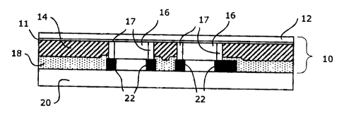
Reference is first made to FIG. 1 and 4, which show one embodiment of a
releasably
mountable electronics component 10 according to the present invention. The
electronics
component 10 comprises a flexible backing or substrate 12 having a mounting
surface 11, a
spacing member 14, electronic modules 16, and an adhesive layer 18. In FIG. 1,
the
electronics component 10 is mounted to a substrate 20 having a number of
electrical contacts
22 and 22A on which electronics components or modules may be mounted. The
electrical
contacts may be connecting pads, leads or conductive traces. In the shown
embodiment, the
electrical contact 22A is a conductive trace. In some embodiments, the
substrate 20 is a
printed circuit board, however it may be any type of substrate capable of
receiving electrical
components or modules.
The backing 12 supports and protects the electronic modules 16. In some
embodiments, the backing 12 is flexible yet sufficiently strong to support the
electronic
modules 16. In some embodiments, the backing 12 may also have ridges or ribs
(not shown)
to increase the strength of the backing 12. The spacing member 14 formed of a
flexible,
non-conductive material. In the shown embodiment, an adhesive is provided on
the
mounting surface 11 of the backing 12 for mounting the spacing member 14 and
electronic
modules 16 thereto.
Each electronic module 16 includes a body and electrical contacts 17 such as
leads.
The electronic modules 16 may be surface mounted components, such as, for
example, light
emitting diodes (LEDs), resistors, capacitors, switches, processors,
microcontrollers, memory
devices, semiconductor chips or integrated circuit chips. As will be
appreciated by one of
ordinary skill in the art, the present invention is not limited to any
specific type of electronics
component and may be used with other types of surface mountable devices.
The adhesive layer 18 extends between the electronic modules 16 and covers at
least
a portion of the spacing member 14. The adhesive layer 18 may be a ready-to-
use adhesive
that does not requiring curing or setting. In some embodiments, the adhesive
layer 18 is
formed of a re-useable or non-permanent adhesive that allows the component 10
to be
removed and (re)mounted several times. The adhesive layer 18 may be formed of
a non-
CA9-2004-O 130 4
CA 02490676 2004-12-16
conductive adhesive to reduce the formation of short circuits.
In the shown embodiment, the regions between the electronic modules 16 and the
electrical contacts 22, 22A are bare of adhesive providing an air gap or space
between the
electrical contacts 22 when the component 10 is mounted. The adhesive layer 18
may be
applied using masking techniques so that adhesive is only applied to the
spacing member 14
or backing 12, leaving the electrical contacts 17 of the electronic modules 16
exposed. When
the electronics component 10 is mounted to the substrate 20, the modules 16
and electrical
contacts 22 are placed in direct physical contact which provides an electrical
connection
between them. In other embodiments, an electrically conductive contact aid may
overlay the
electrical contacts 17 to improve the electrical connection between the
electronic modules 16
and the electrical contacts 22. For example, the electrical contacts 17 may be
coated with a
conductive paste, gel, or cream. The component 10 may be configured to provide
a gap or
recess for receiving the contact aid in the region opposite the electrical
contacts 17. When
the electrical component 10 is attached to the substrate 20, the conductive
paste will improve
the contact between the electrical contacts of the component 10 and substrate
20, thereby
improving the electrical connection. In other embodiments, an electrically
conductive
adhesive covers the electrical contacts 17 of the electronic modules 16. The
electrically
conductive adhesive permits a releasable/removable connection between the
electrical
contacts 1? and the electrical contacts 22 and improves the electrical
connection
therebetween. In some embodiments, an electrical contact may be printed on an
outer
surface of the electrically conductive adhesive using conductive ink or other
suitable
material.
The releasably mountable electronics component 10 may also have a protective
covering (not shown) which overlays the adhesive layer 18. The protective
cover may be
made of a release material such as Teflon~ to provide an easily removable
covering. During
mounting or installation of the releasably mountable electronics component 10,
the protective
covering is removed by, for example, peeling off the protective covering to
expose the
adhesive layer 18.
The shape and size of the backing 12 or the "footprint" of the releasably
mountable
CA9-2004-013 0 5
CA 02490676 2004-12-16
electronics component may be sized and configured to match the electronic
module. For
example, in applications where the electronics component includes only one
electronic
module, the size of the backing and therefore the electronics component may be
the same as
that of the electronic module.
In some embodiments, the outer surface of the backing 12 may have images
and/or
text or other indicia printed or otherwise received thereon. The images and
text may contain
any desired representations, and in some embodiments, may include indications
of
orientation, such as arrows, for use by an end user when the electronics
component is
mounted to a substrate.
Reference is next made to FIG. 2, which shows another embodiment of a
releasably
mountable electronics component 40 according to the present invention. The
releasably
mountable electronics component 40 comprises a flexible backing or substrate
42 having a
mounting surface 41, upper and lower spacing members 44A and 44B, a first
electronic
module 45, a second electronic module 46, and an adhesive layer 48. A circuit
or conductive
trace 47 may also be provided. In FIG. 2, the electronics component 40 is
mounted to a
substrate 50 having a number of electrical contacts such as electrical
contacts 52 on which
electronics components or modules may be mounted. In some embodiments, the
substrate 50
is a printed circuit board, however it may be any type of substrate capable of
receiving
electrical components or modules.
The adhesive layer 48 extends between the electronic modules 45, 46 and covers
at
least a portion of the lower spacing member 44B. The adhesive layer 48 may be
a ready-to
use adhesive that does not requiring curing or setting. In some embodiments,
the adhesive
layer 48 is formed of a re-useable adhesive that allows the component 40 to be
removed and
(re)mounted several times. The adhesive layer 48 may be formed of a non-
conductive
adhesive to reduce the formation of short circuits.
An electrically conductive adhesive 49 covers the electrical contacts 43 of
the
electronic modules 45, 46. The electrically conductive adhesive 49 permits a
releasable/removable connection between the electrical contacts 43 and the
electrical contacts
52 and improves the electrical connection therebetween. In the shown
embodiment, an air
CA9-2004-013 0 6
CA 02490676 2004-12-16
gap or space is provided between the electrical contacts 52 of the substrate
50 in the area in
front of or opposite the electronic module 45.
In some embodiments, an electrical contact may be printed on an outer surface
of the
electrically conductive adhesive 49 using conductive ink or other suitable
material. Masking
techniques may be used to apply the adhesive when manufacturing the component
40 to
create electrically conductive regions (i.e. the adhesive 49) overlaying the
electrical contacts
43 of the electronic modules 45, 46 while being substantially non-conductive
elsewhere (i.e.
the adhesive layer 48).
The backing 42 supports and protects the electronic modules 45, 46. In some
embodiments, the backing 42 is flexible yet sufficiently strong to support the
electronic
modules 45, 46. In some embodiments, the backing 42 may also have ridges or
ribs (not
shown) to increase the strength of the backing 42. The spacing members 44A and
44B are
formed of a flexible, non-conductive material, and are held together, for
example, using an
adhesive.
Each electronic module 45, 46 includes a body and electrical contacts 43 such
as
leads. The electronic modules 45, 46 may be surface mounted components, such
as, for
example, light emitting diodes (LEDs), resistors, capacitors, processors,
microcontrollers,
memory devices, semiconductor chips or integrated circuit chips. As will be
appreciated by
one of ordinary skill in the art, the present invention is not limited to any
specific type of
electronics component and may be used with other types of surface mountable
devices. In
the shown embodiment, the electronic module 45 is a standard or "off the
shelfl' SMD and
the electronic module 46 is a semiconductor package such as JEDEC Code S-PLGA-
N or S-
PDSO-N package.
The conductive trace 47 may be printed on the mounting surface 41 or one of
the
spacing members 44A, 44B, or may be provided on a separate circuit, such as a
flexible
printed circuit. In some embodiments, the flexible circuit is disposed between
the spacing
members 44A and 44B or between the backing 42 and the electronic modules 45,
46. In the
shown embodiment, the conductive trace 47 is provided between the spacing
members 44A
and 44B, however in other embodiments the conductive trace may be positioned
differently.
CA9-2004-O 130 7
CA 02490676 2004-12-16
In this embodiment, the conductive trace 47 is printed on a lower surface of
the lower
spacing member 44B. An electrical contact 43A connects the conductive trace 47
to the
conductive adhesive 49 and electrical contacts 52 of the substrate 50.
Conductive traces and methods of forming conductive traces will be familiar to
one
skilled in the art. In some applications, the conductive trace may be wider
than a typical
SMD or at least wider than the electrical contacts of an SMD, facilitating
(re)installation of
the releasably mountable electronics component without significant issues
regarding
alignment between the electrical contacts of the electronic modules and the
conductive trace.
Reference is next made to FIG. 3, which shows another embodiment of a
releasably
mountable electronics component 60 according to the present invention. The
releasably
mountable electronics component 60 comprises a flexible backing or substrate
62 having a
mounting surface 61, a spacing member 64, electronic module 66, and an
adhesive layer 68.
In FIG. 3, the electronics component 60 is mounted to a substrate 70 having a
number of
electrical contacts such as electrical contacts 72 on which electronics
components or modules
may be mounted. In some embodiments, the substrate 70 is a printed circuit
board, however
it may be any type of substrate capable of receiving electrical components or
modules.
Although not shown, the releasably mountable electronics component 60 may also
include a
circuit or conductive trace similar to the conductive trace 47 described
above.
The backing 62 supports and protects the electronic modules 46. In some
embodiments, the backing 62 is flexible yet sufficiently strong to support the
electronic
modules 66. In the shown embodiment, the backing 62 comprises a flexible
backing layer
and a plurality of spaced apart strengthening ribs 63 oriented on an external
surface of the
flexible backing layer to increase the strength of the electronics component
60. In the shown
embodiment, the electronics component 60 has laterally extending ribs 63,
however the ribs
63 may be oriented differently in different embodiments. For example,
longitudinally
extending ribs may also be used. The ribs 63 may be made of the same material
as the
flexible backing layer, or the ribs 63 may be made of a different material. In
some
embodiments, the ribs 63 are made of a relatively rigid material to provide
increased
strength. The spacing member 64 is formed of a flexible, non-conductive
material.
CA9-2004-O l 30 8
CA 02490676 2004-12-16
Each electronic module 66 includes a body and electrical contacts 67 such as
leads.
The electronic modules 66 may be surface mounted components, such as, for
example, light
emitting diodes (LEDs), resistors, capacitors, switches, processors,
microcontrollers, memory
devices, semiconductor chips or integrated circuit chips. As will be
appreciated by one of
ordinary skill in the art, the present invention is not limited to any
specific type of electronics
component and may be used with other types of surface mountable devices.
The adhesive layer 68 extends between the electronic modules 66 and covers at
least
a portion of the spacing member 64. The adhesive layer 68 may be a ready-to-
use adhesive
that does not requiring curing or setting. In some embodiments, the adhesive
layer 68 is
formed of a re-useable adhesive that allows the component 60 to be removed and
(re)mounted several times. The adhesive layer 68 may be formed of a non-
conductive
adhesive to reduce the formation of short circuits.
An electrically conductive adhesive 69 covers the electrical contacts 67 of
the
electronic modules 66. The electrically conductive adhesive 69 provides a
releasable/removable connection between the electrical contacts 67 and the
electrical contacts
72 and improves the electrical connection therebetween. In the shown
embodiment, an air
gap or space is provided between the electrical contacts 72 of the substrate
70 in the area in
front of or opposite the electronic modules 66.
In some embodiments, an electrical contact may be printed on an outer surface
of the
electrically conductive adhesive 69 using conductive ink or other suitable
material. Masking
techniques may be used to apply the adhesive when manufacturing the component
60 to
create electrically conductive regions (i.e. the adhesive 69) overlaying the
electrical contacts
67 of the electronic modules 66 while being substantially non-conductive
elsewhere (i.e. the
adhesive layer 68)
In some embodiments, an advantage of the present invention is that an
electronics
component may be replaced with relative ease by end users of electronic
devices without
soldering equipment or the use of sockets as is typically required when
replacing electronics
component such as surface mounted devices (e.g. LEDs). In one example
embodiment, the
releasably mountable electronics component may be used to repair or modify
consumer
CA9-2004-O l 30
CA 02490676 2004-12-16
electronics devices by an end user. Many electronics devices are now designed
to allow the
purchaser or end user to perform limited after-market modifications. Using the
present
invention, for example, the LED backlight of a phone, such as a cellular
phone, may be
replaced to modify the colour of the LED backlight. According to some example
embodiments, a user may remove an existing LED-based releasably mountable
electronics
component by peeling off a releasably mountable electronics component from its
underlying
substrate or circuit board, and replacing it with another having an LED with
the colour of the
user's choice.
In other applications, releasably mountable electronics components constructed
according to the present invention may be used for processors operating at
relatively high
frequencies. At higher frequencies, the conventional pin or socket used to
connect a
processor to a circuit board becomes more sensitive to radio frequency (RF)
and may act as a
small antenna. As the releasably mountable electronics component does not
contain
components which are particularly sensitive to RF, this problem may be
mitigated or
1 S eliminated in some applications.
In some embodiments, the releasably mountable electronics component may
provide
a component that is thinner than conventional replaceable processors which
typical use a pin
or socket design, exhibits reduced interference from RF, and has lower
production costs.
Further, in some embodiments, the releasably mountable electronics component
may provide
improved heat dissipation as a result of increased surface area on both sides
of the
component relative to conventional processors where the socket side cannot
typically
dissipate heat effectively due to the presence of a large air gap. In some
applications, the
releasably mountable electronics component provides improved repair
characteristics and
relatively high connection strength between the substrate or circuit board to
which it is
mounted.
In some embodiments, the electronic modules of the releasably mountable
electronics
component may be more complex circuits. For example, in some example
embodiments a
wireless network card module may be used.
Another application of releasably mountable electronics component constructed
CA9-2004-O l 30 10
CA 02490676 2004-12-16
according to the preset invention is in custom circuit design. For example,
the releasably
mountable electronics component may be used for educational purposes. A
circuit may be
designed and prepared by a student, for example, by forming a conductive trace
on a suitable
substrate. The conductive trace may be formed using a conductive pen, such as
those sold
under the Circuit WorksTM trade name. Conductive trace pens contain an air
drying
conductive trace fluid. Conductive trace pens are often silver based.
Depending on the
particular pen selected and the size of its tip, the trace may be relatively
small allowing finer
circuits to be prepared. One or more releasably mountable electronics
components having
discreet electronic modules may then be mounted on to the conductive circuit
trace to
complete the circuit.
The present invention may be embodied in other specific forms without
departing
from the spirit or essential characteristics thereof. Certain adaptations and
modifications of
the invention will be obvious to those skilled in the art. Therefore, the
presently discussed
embodiments are considered to be illustrative and not restrictive, the scope
of the invention
being indicated by the appended claims rather than the foregoing description,
and all changes
which come Within the meaning and range of equivalency of the claims are
therefore
intended to be embraced therein.
CA9-2004-O 130 11