Note: Descriptions are shown in the official language in which they were submitted.
CA 02491084 2004-12-24
WO 2004/004136 PCT/US2003/020055
FREQUENCY HOPPING SPREAD SPECTRUM DECODER
FIELD OF THE INVENTION
[0001] The present invention relates generally to the field of
cormnunications. More
particularly, the invention relates to a frequency hopping spread spectrum
technique for
accepting and sorting complex waveforms to lock onto a desired remote signal.
BACKGROUND OF THE INVENTION
[0002] Fixed network communication systems may operate using wire line or
radio
technology. Wire line technologies include utilizing the utility distribution
lines and/or
telephone lines. Wireless technologies may utilize the 902-928 MHz range,
which can
operate without a FCC license through the use of frequency hopping spread
spectrum
(FHSS) transmission, which spreads the transmitted energy over the band.
According to
FCC Regulations, for frequency hopping systems operating in the 902-928 MHz
band,
total output is as follows: 1 watt for systems employing at least 50 hopping
channels;
and, 0.25 watts for systems employing less than 50 hopping channels, but at
least 25
hopping channels. See, 47 U.S.C. ~ 15.247.
[0003] FHSS systems meet the FCC specification by communicating to remote
communication devices in synchronization, both in time and frequency. Using
this
approach, all devices know when to hop to the next channel in the sequence and
what the
next sequence channel is. A known FHSS system utilizes a hop rate that is
faster than
the data rate to send multiple sets of randomly selected frequencies in each
message to
distribute the transmitted energy over the communication band. This
distribution is one
of the FCC requirements to operate in the ISM band.
[0004] A disadvantage of the above is that it requires all devices to include
a real time
clock, which adds to the cost of the device. In addition, some type of battery
storage
system is required to maintain the real time clock in the event power should
be removed
from the device. Further, the requirement to step rapidly through the
frequencies
constrains the design of such devices and further limits cost reduction.
[0005] There have been attempts to utilize remote devices that operate
asynchronously
that gain synchronization with the transmitter by using a scanning receiver.
One
example of such a receiver is that of Harmon, U.S. Patent No. 4,328,581.
However,
spurs and other unwanted signals interfere with the synchronization process in
such
-1-
CA 02491084 2004-12-24
WO 2004/004136 PCT/US2003/020055
receivers. Another problem with such systems is that the receiver is scanning
channels
based on a list and may be scanning channels other than the channel on which a
preamble is being sent. To compensate for this, the transmitter must send the
preamble
for a period of time long enough to allow the receiver to scan for it and
develop a bit
timing. In these systems, spurs may be decoded as valid preambles, which
adversely
affects performance. Further, crosstalk problems may arise if weak signals
from the
transmitter are captured in the receiver scan sequence prior to determining
the desired
transmit channel.
[0006] Therefore, there is a need for a FHSS communication device that is cost
efficient,
meets FCC requirements for power distribution in the ISM band, and includes
provisions
for preventing unwanted signals from capturing the scanning receiver. The
present
invention is directed to these, as well as other, needs in the art.
SUMMARY OF THE INVENTION
[0007] The present invention addresses the needs identified above in that it
provides for
a novel method and apparatus that utilizes frequency hopping spread spectrum
communications. In accordance with the present invention, there is provided an
asynchronous frequency hopping spread spectrum receiver that includes an
integrated
circuit transceiver providing a PLL lock signal and a received signal strength
indicator
signal, and a microcontroller that receives the PLL lock signal and the
received signal
strength indicator signal. The receiver scans a predetermined list of channels
and the
microcontroller converts the received signal strength indicator signal for
each scanned
channel to a digital value representative of the received signal strength
indicator signal
and stores each the digital value in a received signal strength indicator
list. The
microcontroller next determines a subset of channels to scan for a preamble
pattern. The
subset of channels may be determined from a predetermined number of highest
digital
values stored in the received signal strength indicator list.
[0008] In accordance with a feature of the invention, the microcontroller
rescans the
predetermined list of channels a predetermined number of times and determines
the
subset of channels from the highest digital values after completing the
predetermined
number of rescans. A channel corresponding to a highest digital value
contained in the
subset of channels is scamzed for the preamble pattern. If the channel
corresponding to
the highest digital value does not contain the preamble pattern, a next
channel
-2-
CA 02491084 2004-12-24
WO 2004/004136 PCT/US2003/020055
corresponding to a next highest value in the subset of channels is scanned for
the
preamble pattern.
[0009] In accordance with another aspect of the invention, there is provided a
method of
scanning for a preamble bit pattern in an asynchronous frequency hopping
spread
spectrum receiver. The method includes scanning a predetermined list of
channels;
converting a received signal strength indicator signal for each scanned
channel to a
digital value representative of the received signal strength indicator signal;
storing the
digital value in a received signal strength indicator list; and determining a
subset of
channels to scan for a preamble pattern, the subset of channels being
determined from
channels corresponding to a predetermined number of highest digital values
stored in the
received signal strength indicator list.
[00010] In accordance with yet another aspect of the invention, there is
provided a process
for scanning for a preamble bit pattern in an asynchronous frequency hopping
spread
spectrum receiver. The process includes scanning a predetermined list of
channels a
plurality of times to determine a subset of channels having higher signal
strengths
relative to all channels in the predetermined list, and successively scanning
each channel
within the subset of channels for a preamble bit pattern beginning with a
channel having
the highest signal strength until the preamble pattern is found.
[00011 ] These and other aspects of the present invention will be described in
the
following detailed description of the invention.
BRIEF DESCRIPTION OF THE DRAWINGS
[00012] The foregoing surmnary, as well as the following detailed description
of the
preferred embodiments, is better understood when read in conjunction with the
appended
drawings. For the purpose of illustrating the invention, there is shown in the
drawings an
embodiment that is presently preferred, in which like references numerals
represent
similar parts throughout the several views of the drawings, it being
understood, however,
that the invention is not limited to the specific methods and
instrumentalities disclosed.
In the drawings:
[00013 ] Fig. 1 illustrates an overview of an exemplary embodiment of a
frequency
hopping radio in accordance with the present invention;
[00014] Fig. 2 illustrates an exemplary receive signal strength indicator
(RSSI' scan
process;
[00015] Fig. 3 illustrates an exemplary two scan process for ranking the RSSI;
-3-
CA 02491084 2004-12-24
WO 2004/004136 PCT/US2003/020055
[00016] Fig. 4 illustrates an exemplary carrier detect process;
[00017] Fig. 5 illustrates an exemplary carrier detect verification process;
[00018] Fig. 6 illustrates an exemplary carrier lock process; and
[00019] Fig. 7 illustrates an exemplary start frame delimiter and bit sampling
process.
DETAILED DESCRIPTION OF THE PREFERRED EMBODIMENTS
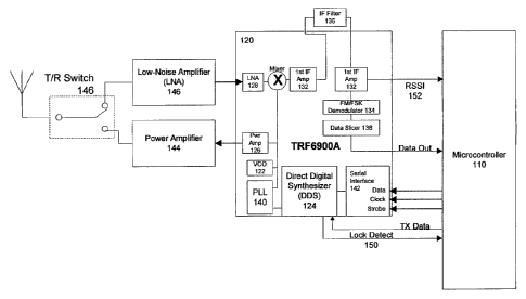
[00020] Referring now to FIG. l, there is illustrated an exemplary embodiment
of a
frequency hopping radio 100 in accordance with the present invention. The
present
invention is controlled by a microcontroller 110 and preferably implemented
using a
Texas Instruments TRF6900 transceiver 120, which is an integrated circuit that
includes
an FSK transceiver to establish a frequency-agile, half duplex, bi-directional
RF link.
The chip may be used for linear (FM) or digital (FSK) modulated applications
in the
North American 915-MHz ISM band.
[00021] The transmitter portion of the transceiver 120 consists of an
integrated voltage
controlled oscillator (VCO) 122, a complete fully programmable direct digital
synthesizer 124, and a power amplifier 126. The receiver portion consists of a
low-noise
amplifier 128, mixer 130, IF amplifier 132, limiter, FM/FSK demodulator 134
with an
external LC tank circuit 136, and a data sliver 138.
[00022] The demodulator 134 may be used for analog (FM) and digital (FSK)
frequency
demodulation. The data sliver 138 preferably acts as a comparator. The data
sliver 138
provides binary logic level signals, derived from the demodulated and low pass-
filtered
IF signal, that are able to drive external CMOS compatible inputs in the
microcontroller
110. The noninverting input is directly connected to an internal reference
voltage and the
inverting input is driven by the output of the low-pass filter amplifier/post
detection
amplifier. The decision threshold of the data sliver 128 is determined by the
internal
reference voltage.
[00023] The direct digital synthesizer (DDS) 124 is based on the principle of
generating a
sine wave signal in the digital domain. The DDS 124 constructs an analog sine
wavefonn using an N-bit adder counting up from 0 to 2 N in steps of the
frequency
register to generate a digital ramp waveform. Each number in the N-bit output
register is
used to select the corresponding sine wave value out of the sine lookup table.
After the
digital-to-analog conversion, a low-pass filter is preferably used to suppress
unwanted
spurious responses. The analog output signal can be used as a reference input
signal for a
-4-
CA 02491084 2004-12-24
WO 2004/004136 PCT/US2003/020055
phase locked loop 140. The PLL circuit 140 then multiplies the reference
frequency by a
predefined factor.
[00024] The microcontroller 110 uses a three-wire unidirectional serial bus
(Clock, Data,
Strobe) 142 to program the transceiver 120. The internal registers contain all
user
programmable variables including the DDS frequency setting registers as well
as all
control registers. At each rising edge of the Cloclc signal, the logic value
on the Data
terminal is written into a 24-bit shift register. Setting the Strobe terminal
high loads the
programmed information into the selected latch.
[00025] The microcontroller 110 controls the transceiver 120 and controls the
transmission and reception of data. The rnicrocontroller 110 also controls
which channel
the radio 100 listens to, or transmits on, by setting registers in the DDS
124. The DDS
124 registers, in turn, control the phase locked loop 140 and the VCO 122 to
set the
transmit and receive frequencies. Those skilled in the art will recognize that
this is one of
several possible methods for setting the transmit and receive frequencies.
[00026] In transmit mode, the transceiver 120 has a transmit output power of 0
dBm. An
external Power Amplifier (PA) 144 provides an additional 24 dB of gain,
resulting in a
total output power of +24 dBm. The microcontroller 110 drives a
Transmit/Receiver
switch 146, which advantageously allows one antenna to be used for both the
transmitter
and receiver portions of the transceiver 120.
[00027] In receive mode, an external low noise amplifier (LNA) 148 and the
internal
LNA 128 are used to amplify the received signal. The received signal is "mixed
down"
by the mixer I23 for processing and then amplified. The signal strength
indicator 152 is
an output and is monitored by the microcontroller 110. The receiver then
converts from
a frequency-modulated signal to baseband signal using the demodulator 134 and
the data
dicer 138. The microcontroller 110 is responsible for decoding the raw
baseband signal,
synchronizing to bit edges.
[00028] As will be described in greater detail below, in receive mode, the
microcontroller
110 uses the Serial W terface 142 to set the receive frequency and then looks
for a valid
preamble from a remote transmitting device. The process of looking for a valid
preamble involves first scanning all 25 channels looking for single strength
on one or
more of the 25 channels. After scanning the channels and sorting the possible
preamble
channels based on RSSI, the receiver attempts to detect a valid preamble on
the channel
with the strongest RSSI. If a valid preamble is not detected, the
microcontroller 110 uses
the Serial Interface 142 to change the frequency to the channel with the next
highest
-5-
CA 02491084 2004-12-24
WO 2004/004136 PCT/US2003/020055
RSSI value. If no preamble is detected, the microcontroller "hops" channels
every 1 ms.
Other hop timing may be used. When a valid preamble is detected, the receiving
device
can synchronize with the transmitter to receive a packet of information, as
detailed
below. Synchronization involves hopping in synch with the transmitter to
additional
preamble and data channels.
[00029] A Lock Detect signal 150 from the transceiver 120 indicates that the
radio 100 is
locked on the desired receive frequency. After writing the Serial Interface
142, which
instructs the radio 100 to change the receiver channel, the microcontroller
110 waits for
Lock Detect 150 to be asserted, signaling the receive chamzel can be monitored
for a
stable received signal. This settling time, in addition to the time required
to write the
registers via the Serial Interface 142, determines the per channel scan time
(e.g., 1 ms).
[00030] An exemplary embodiment implemented using the radio 100 will now be
explained. The present invention does not require a separate clock or other
synchronization information, nor does it require an indication of a valid
signal from the
transceiver 120 to decode the incoming signal. The microcontroller 110
performs the
tasks of decoding and validating the signals, where each signal preferably
contains a
preamble, start frame delimiter (SFD) and a data frame. The SFD indicates that
the
preamble has ended and that the data frame will follow. In accordance with the
present
invention, the SFD must appear within a predetermined maximum time after the
start of
the preamble in order for a signal to be considered valid. Following receipt
of a valid
SFD, the microcontroller 110 maintains bit timing and records the data bits.
[00031] Referring now to Fig. 2, a Received Signal Strength Indictor Scan
process of the
overall decoding process of the present invention will now be described. The
decoding
process involves sampling the incoming signal rapidly and correlating a set of
samples
with a known pattern to determine if a preamble is present. In accordance with
the
present invention, the preamble preferably begins with a zero and ends with a
one.
[00032] The process begins by setting a counter (x) to zero, then at step 200,
a timer in the
microcontroller 110 is started and a channel is selected. The channel is
selected
sequentially from a list of channels (e.g., 25 channels) to be scanned. At
step 202, the
microcontroller 110 tests the PLL lock detect indicator 150 at intervals equal
to a bit time
(e.g., 56.48 ~,s) until a lock is established. Once a lock is established at
step 202, the
timer is set at step 204 to allow the receiver to settle for a configurable
settling time,
where the present invention uses an RSSI settling time of 200 ~,s. At step
206, the
Receive Signal Strength Indicator (RSSI) 152 is monitored by the
microcontroller 110
-6-
CA 02491084 2004-12-24
WO 2004/004136 PCT/US2003/020055
using an analog-to-digital converter within the microcontroller 110. The
microcontroller
110 stores the results of the converted RSSI indicator 152 in a list that
corresponds to the
channel list noted above by position and length. At step 207, a channel
counter value (x)
is incremented by one and then tested to see if it is greater than or equal to
25. If x is less
than 25, processing returns to step 200 to sample the next chaimel. If the
counter is equal
to or greater than 25, then processing exits to search the list (see, Fig. 3)
that was created
through the process of Fig. 2.
[00033] Refernng now to Fig. 3, there is illustrated the carrier detect
portion of the
decoding process of the present invention. At step 208, the RSSI list created
at step 206
is searched for the largest value that is greater than a configurable RSSI
theshold. . This
value corresponds to the strongest signal, as noted above. If a value greater
than the
RSSI threshold is not found, then the RSSI scan process of Fig. 2 is repeated.
At step
210, the largest value determined is replaced with a zero. Next, at step 212,
the offset
into the RSSI list of the signal determined at step 208 to have the largest
value is
calculated and used to select a chamlel value at the same offset into the
channel list. The
transceiver 120 is then set to receive on this channel. For example, if the
signal
determined in step 208 is the ninth channel in the RSSI list, the transceiver
will be set to
the ninth channel on the channel list. At step 214, the PLL lock 150 is tested
at intervals
equal to the bit time (56.48 ~,s) until the lock is established.
[00034] At step 216, a timer in the microcontroller 110 is set to trigger at a
time equal to
11 bit times (e.g., 11*56.48 ~,s). At step 218, the signal on the channel
determined in
step 212 is sampled for two preamble bit times (e.g., 2*56.48 p,s). In
accordance with
the present invention, 32 samples over the two preamble bit times are
recorded.
Alternatively, sub-samples may be recorded between samples and used to form
samples
by simple voting if processor speed allows.
[00035] At step 220, the samples are analyzed as two 16 sample halves. Each
half is
compared with 16 ideal patterns. Tn accordance with the present invention, the
ideal
patterns are generated from the 16 rotations of OxF00F. At step 222,
correlation is
performed by performing an XOR (exclusive OR) operation on the four bytes of
the
samples with each of the four bytes of the ideal pattern. The number of bit
positions in
which the samples and pattern differ (Hamming distance) is the number of
correlation
errors for that pattern. The number of ones in the XOR result is the number of
errors and
is preferably calculated using the sum of four lookups in a 256-byte table
containing the
number of ones in each index byte. The number of rotations needed to achieve
the
CA 02491084 2004-12-24
WO 2004/004136 PCT/US2003/020055
pattern with the fewest errors is stored by the microcontroller 110. If the
number of
correlation errors is within a configurable tolerance, the signal is
considered to be a
preamble candidate. The present invention uses a default tolerance of 3 bit
errors. If the
number of correlation errors is greater than the tolerance, the carrier detect
process of
Figure 3 is repeated, using the channel with the next highest RSSI value. If
this next
highest RSSI value does not exceed the RSSI threshold, the process restarts at
Figure 2.
[00036] At step 224, the value of a free running timer set at step 216 is used
to compute a
time offset to the next occurrence of the identical pattern in accordance with
the number
of pattern matching rotations stored at step 222. The pattern is matched to
one of a list of
patterns and the time adjustment is performed such that the carrier detect
verification
(i.e., repeating the 32 samples looking for valid preamble) is now aligned
with the
pattern that was found on the first attempt. In other words, the timer is
adjusted so that an
ideal carrier detect verification matches the pattern from the first Garner
detect.
[00037] Fig. 4 illustrates a carrier detect verify process, which occurs over
two bit times
of sampling. At step 226, when the timer set at step 216 (Fig. 3) expires,
another timer
in the microcontroller is set to expire in six bit times (6*56.48 p,s). At
step 228, the
signal on the transceiver channel set at step 212 is sampled for two bit times
(2*56.48
~s). 32 samples over the two preamble bit times are recorded by the
microcontroller
110. As described above, sub-samples may be recorded between samples and used
to
form samples by simple voting if processor speed allows.
[00038] Also at step 230, the 32 samples are analyzed as two 16 sample halves
and
compared to the pattern recorded at step 222 (Fig. 3). The sample must contain
less than
the number of configurable correlation errors plus two. If the errors in the
sample are
found to exceed the limit, the carrier detect process of Fig. 3 is repeated
using the
channel with the next highest RSSI value. If this next highest RSSI value does
not
exceed the RSSI threshold, the process restarts at Figure 2..
[00039] At step 232, the free running timer set at step 226 is adjusted to
expire in order to
center the sampling period in a carrier lock process (described below with
reference to
Fig. 5) across a down edge of a preamble bit. The free running timer is
adjusted in
accordance with a value computed using the number of pattern rotations stored
at step
222.
[00040] Refernng now to Fig. 5, there is illustrated the carrier lock process
of the present
invention. At step 234, a timer is set to expire after a time period equal to
seven bit times
(7*56.48 p,s). At step 236, 16 samples over one-half of a preamble bit time
beginning
_g_
CA 02491084 2004-12-24
WO 2004/004136 PCT/US2003/020055
one-quarter of a bit time prior to the previously inferred location of the
down edge are
recorded. The location was inferred through the carrier detect and carrier
detect verify
processes, described above.
[00041] At step 238, the 16 samples are correlated with 15 ideal preamble
patterns and 15
inverted ideal preamble patterns, which are stored in a table. The table is
preferably
organized to represent inverted preamble patterns at one end of the table and
preamble
patterns at the other end. The patterns are in a sequence that represents the
desired
pattern shifted to the left and then right by one bit, two bits, etc. In each
successive
carrier lock, the starting point in the table is adjusted in order to refine
the timing to
avoid failure. A pattern match in the inverted portion of the table indicates
the beginning
of the SFD.
[00042] At step 240, if the number of correlation errors is within the
predetermined
tolerance for the preamble correlation pattern, the signal is considered to be
a preamble
candidate by the microcontroller 110. The timer set at step 234 is adjusted to
center on
the next down edge and the process repeats.
[00043] If at step 240 the number of correlation errors is within the
predetermined
tolerance for the SFD correlation pattern, the SFD has started. Bit sampling
is performed
to find the rest of the SFD pattern as described b elow with reference to Fig.
6. The
tolerances for Garner lock is preferably the same in both cases, regardless of
whether a
preamble bit or a SFD bit is being detected. The tolerance is configurable,
but the present
invention uses a default of 3 bit errors.
[00044] If a total of two carrier lock preamble correlation attempts fail or
the total
preamble time before the SFD is exceeded, the signal is no longer considered a
preamble
candidate and the decoding process returns to perform the RSSI scan of Fig. 2.
[00045] Referring now to Fig. 6, there is illustrated the SFD and bit sampling
process of
the present invention. At step 242 a bit-center timer is started to trigger in
the middle of
each half bit. Herein, a bit is a Manchester encoded bit made up of two half
bits of one-
half bit time. Manchester Encoding is well known in the art an encodes a logic
0 by
indicated by a 0 to 1 transition at the center of a bit and a logic 1 by
indicating a 1 to 0
transition at the center of a bit.
[00046] At step 244, the half bit is sampled as many times a possible in
accordance with
processor speed. It is preferable to begin sampling one-half of a sample
period prior to
the half bit center.
_9_
CA 02491084 2004-12-24
WO 2004/004136 PCT/US2003/020055
[00047] At step 246, equal numbers of samples from each half of the Manchester
bit are
voted by bit-wise first inverting the first samples and then counting the
number of
samples of the 16 that are ones. If fewer than half axe ones, the Manchester
bit is
considered a zero data bit. If half or more are ones, then the Manchester bit
is considered
to be a one data bit.
[00048] In accordance with the present invention, the SFD is composed of 32
Manchester
one bits followed by the following Manchester bits: 0000 1100 1011 1101 (left
bit first).
Other sequences of bits may be used. No bit errors are tolerated in the SFD.
If the SFD
is not found, then the RSSI scan of Fig. 2 is repeated.
[00049] After the SFD found, the transceiver 120 is in synchronization with
the
transmitter, and continues to sample the bits to receive the data from
transmitted by the
transmitter. . '
[00050] Refernng now to Fig. 7, in accordance with an aspect of the present
invention, a
two-step RSSI scan process may be implemented to determine which of the
channels is
the appropriate data chamlel. At step 300, the first scan is performed wherein
the
receiver scans the complete list of channels, quantifies the RSSI indicator
152 and sorts
the list for the strongest RSSI levels. A subset of the strongest channels
(e.g., 3
channels) may be developed from this first scan of the channels. The subset of
channels
may consist of more or less channels than three.
[00051] At step 302, the first scan is repeated a predetermined number of
times, e.g., four
times, where a subset of strongest chaimels is developed for each scan. The
scan may be
repeated an alternate number of times. At the completion of the final RSSI
first scan, the
strongest channels from all of the scans are sorted by RSSI level.
[00052] At step 304, a second scan is performed wherein a scan is performed of
the
highest RSSI level, as determined by the first scan process above. At step
306, the
strongest signal is analyzed for preamble and a start frame delimiter (SFD)
bit patterns
that will further qualify the channel as the transmit channel. The process of
determining
if the SFD bit patterns are present in a particular channel has been described
in the
preceding paragraphs. If the preamble bit patterns are not present, then the
second
strongest channel and so on is analyzed for valid preamble and SFD bit
patterns until
found. If the preamble bit pattern is not found during the second scan
process, the first
scan process is repeated.
[00053] Various modifications of the invention, in addition to those described
herein, will
be apparent to those of skill in the art in view of the foregoing description.
Such
-10-
CA 02491084 2004-12-24
WO 2004/004136 PCT/US2003/020055
modifications are also intended to fall within the scope of the appended
claims. For
example, a bit time other than 56.48 ~,s may be used. In addition, bits may be
encoded
using an encoding scheme other than Manchester Encoding.
-11-