Note: Descriptions are shown in the official language in which they were submitted.
CA 02491119 2004-12-23
WIDEBAND SIGNAL GENERATORS, MEASUREMENT DEVICES,
METHODS OF SIGNAL GENERATION, AND METIiODS OF
SIGNAL ANALYSIS
RELATED APPLICATIONS
[000I] This application claims the benefit of United States Patent
Application No. 10/624,900, filed July 23, 2003, and of International (PCT)
Patent Application No. XXX, filed December 11, 2003 by deposit at the U.S.
Patent and Trademark Office and naming as inventors P.K.W. Jackson and
D.S. Hardy (attorney docket no. 19621130720.
FIELD OF THE INVENTION
[0002] The present invention relates to signal generators, frequency
synthesizers, devices incorporating signal generators andlor frequency
synthesizers, and methods of signal generation.
BACKGROUND
[0~3] Many electronics applications and systems require the use of
one or more signals having particular frequencies and/or phases. For example,
radio transmitters and receivers frequently employ local oscillator signals
for
upconversion and downconversion. Accordingly, methods and devices have
been developed for generating such signals, including phase locked loop
(PLL) based solutions.
[0004] Another device that may be used to generate signals is the
direct digital synthesizer (DDS), Typically, a DDS receives an input clock
signal and a contml word. Based on the control word and possibly also on
CA 02491119 2004-12-23
subsequent timing (Read, Write, Update control, etc.), the DDS outputs a
waveform (e.g., a sine wave) having a known frequency and/or phase with
respect to the input clock signal. For example, a DDS generally includes a
phase accumulator to indicate a phase state of the current output sample and a
lookup table to indicate an amplitude corresponding to that phase state. The
control word may be loaded into a register of the DDS such as, for example,
an accumulator. The DDS then determines the desired frequency and/or phase
of the output signal based on the lookup table information associated with the
received input control word. DDS devices available from integrated circuit
suppliers include the AD98XX series products available from Analog Devices,
Inc. of Norwood, Massachusetts. Other DDS suppliers include Harris
Corporation of Melbourne, Florida; Intersil Corporation of Melbourne,
Florida; and Intel Corporation of Santa Clara, California.
[0005) A staadard DDS may include a phase accumulator, a phase-to-
amplitude converter, and a Digital to Analog Converter (DAC). The DDS
core described above without the DAC iriay also be referred to as a
Numerically Controlled Oscillator (NCO). The phase accumulator, phase-to-
amplitude converter, and DAC are the standard building blocks for the DDS,
although the implementation of each vanes from design to design.
(0006] One such variance is the implementation of the phase-to-
amplitude converter. This converter, which generally uses a look-up table
stored in memory, receives the phase at a given sample and outputs a
corresponding amplitude. However, in such implementations, only the most
significant portion of the phase value may be used due to memory size
limitations of current designs. Therefore the table truncates the X least
significant bits (where X may change from design-to-design and part-to-part),
using only the Y most significant bits. Additionally, the implementation of
the
table may change. For example, the amplitude may be repeated in 90 degree
increments and only the sign of the amplitude may change according to the
CA 02491119 2004-12-23
3
quadrant. Therefore many look-up tables use only 90 degrees in the took-up
table along with a sign bits) to specify what quadrant the phase is in.
(000'1] A DDS may be configwred as a frequency divider. In such
cases, the control word may specify a desired frequency and/or phase of the
output signal (where the frequency is processed through the DDS core and any
phase offset is summed in) as the ratio of the desired output signal to the
input
clock signal (where the output frequency is based on the accumulator value
and the clock rate).
[0008] Because the DDS output is produced using a digital process,
DDS based solutions may provide a significant reduction in phase noise as
compared to analog based solutions. For example, analog solutions may use
an error correction loop to determine the phase/frequency of the output. In
such case, the transfer function that determines the extent (e.g., bandwidth)
of
correction is inversely proportional to the time required to correct, thereby
sacrificing speed for phase noise or vice versa. Furthermore, DDS based
solutions can provide fine tuning resolution of the output frequency (e.g.,
micro-hertz tuning resolution) as well as sub-degree phase tuning. In
addition,
DDS based solutions may provide such advantages as an extremely fast speed
in tuning to the output frequency or phase, phase-continuous frequency
switching with no over/undershoot, and little or no settling time as may occur
for analog based (e.g. loop) solutions. DDS based solutions may also reduce
or eliminate the need for manual system tuning and tweaking due to
component aging and temperature drift, for example, that are often issues for
analog based solutions.
(0009] However, DDS based solutions may require relatively high
input clock speeds and may produce spurious frequency responses in which
unwanted components are present in the output frequency spectrum.
CA 02491119 2004-12-23
4
[0010] One source of spurious output components (or "spurs") is phase
truncation error. Phase truncation error may occur, for example, when the
number of entries in the DDS output lookup table is less than the maximum
number of possible amplitudes capable of being specified by the digital
control word based on, for example, the length of the accumulator register in
the DDS which receives the control word for dccoding. For example, a DDS
with a 32-bit phase accumulator is capable of distinctly specifying 23Z
distinct
phases. To provide corresponding amplitude entries for cach of these 23z
possibilities would require a phase lookup table containing 4,294,967,296
entries, which may not be feasible to provide in a design. Therefore, the
lookup table may include less than the maximum number of possible
amplitudes, and the DDS may resolve or correlate the phase accumulator value
resulting from an input control word to that phase which is closest to the
exact
value specified by the state of the phase accumulator.
[0011] Furthermore, the amplitude of the truncation error spurs may
vary periodically over time based on the overflow characteristic of the phase
accumulator (also known as the Crrand Repetition Rate). The change in
truncation error amplitude with respect to time may define a periodic
waveform having a frequency spectrum of sufficiently high range that higher
order harmonics of the truncation error waveform produce aliasing into the
Nyquist bandwidth. Additional infonmation regarding DDS phase truncation
and other errors and spurious responses is available from industry sources
including, for example, "A Technical Tutorial on Digital signal Synthesis"
(published by Analog Devices, lnc., 1999, available online at
www.analog,comItJpIoadedFilesITutorialsl 3343533079104002517DDStutor.pdf).
[0012] Spurious responses may appear at frequencies relatively close
to the output frcquency of a DDS. This aspect can be particularly troublesome
to system designers. In narrowband applications, the DDS input clock can be
set to a single frequency or a very narrow tuning band, for example, to avoid
CA 02491119 2004-12-23
these "close in" responses. However, thus restricting the range of the input
clock also limits the output signal tuning range of the DDS.
[0013) Errors in the digital-to-analog conversion (DAC) process are
typically a significant source of spurious responses. Such errors may include
quantization error as well as DAC nonlinearities. DAC-introduced error,
which may be related to the clock and the output frequencies, is typically
highly predictable.
SUMMARY
(0014) Embodiments of the present invention include systems and
methods for utilizing DDS based signal generator solutions for wideband
applications. Such embodiments may also provide systems and methods for
reducing or avoiding spurious DDS responses by varying the clock signal
input to the DDS.
[0015] At least one embodiment of a signal generator according to the
present invention includes a clock generator that has a first direct digital
synthesizer (DDS) configured to produce a clock signal based on a clock
source signal. The signal generator fiuther includes a clock divider that has
a
second DDS configured to produce a divided signal based on (1) the clock
signal and (2) a control signal indicating a divide ratio. These embodiments
may further include selectable filters configured to produce a filtered signal
based on the divided signal. The selection among the selectable filters may be
based on the control signal, a selected output frequency (e.g. as selected by
a
user or by a hardware or software component of an application), a frequency
of the divided signal {which may be based on the selected output frequency),
and/or another value based on the selected output frequency such as a divide
ratio. In at least one embodiment, the number of selectable filters is four.
CA 02491119 2004-12-23
6
[0016] In at least one embodiment, the signal generator may further
comprise a frequency translator co~gured to produce a translated signal
based on the filtered signal. The translator may be, in some embodiments, a
mixer receiving a local oscillator (LO) signal, a frequency doubter, or a
multiplier including, for example, a step recovery diode (SRD). Use of a
multiplier may result in spurious components also being translated, however.
[0017] In at least one embodiment, the clock divider may be
configured to produce a divided signal having a principal frequency that is
2.5
times lower than a principal frequency of the clock signal with subsequent
filtering.
[0018] Furthermore, the clock divider may include a third DDS
configured to produce a second divided signal based on (t) the clock signal
and (2) a second control signal indicating a second divide ratio. In such
embodiments, the selection of one of multiple selectable filters may be
provided based on the second control signal. In at least one embodiment, the
number of selectable filters is four.
[0019) In addition, in at least one embodiment the second DDS (or
third DDS) may include a table of output values and the divided signal may be
determined based on the table of output values in response to (t) the clock
signal and (2) a control signet indicating a divide ratio and forgoing the
phase
to amplitude conversion. In these embodiments, the second DDS may output
changes to the divided signal at a firequency substantially equal to the
frequency of the clock signal without the full phase to amplitude conversion.
Because the output divided signal may be an integer or integer +/- a subset
(such as, for example, 0.5) of the phase value, it may be possible to reduce
the
size of the lookup table.
[0020] Furthermore, in at least one embodiment the second DDS (or
third DDS) may be preloaded to output the divided signal at a predefined
CA 02491119 2004-12-23
7
frequency in response to receiving the clock signal (e.g. with substantially
no
delay).
[0021) A method of generating a signal according to another
embodiment of the invention includes using a first DDS to generate a clock
signal and using a second DDS to generate a signal based on the clock signal
and having a frequency that is substantially equal to one-half of the clock
signal. Such a method may also include providing a phase offset value to the
second DDS.
[0022) A method of generating a signal according to another
embodiment of the invention includes providing a first signal to a clock input
of a DDS and using the DDS to generate an output signal based on the first
signal and having a frequency that is substantially equal to one-half of the
clock signal. Such a method may also include providing a phase offset value
to the DDS.
[01123) A method of generating a signal according to another
embodiment of the invention includes using a DDS to generate an output
signal having a desired frequency component and a spurious fi~equency
component, monitoring a strength of the spurious frequency component, and
changing a phase offset value of the DDS based on a result of said monitoring.
[0024) Further embodiments of the invention include transmitters,
receivers, transceivers, test equipment, signal analyzers, spectrum analyzers,
satellite communications systems, modulators, demodulators, and radar
systems that include signal generators as described herein (e.g. employed as
local oscillators), methods of using such devices, methods of signal analysis,
methods of modulation, and methods of demodulation.
BRIEF DESCRIPTION OF THE DRAWINGS
CA 02491119 2004-12-23
g
[0025] The invention described herein is further explained in terms of
exemplary embodiments. These exemplary embodiments are described in
detail with reference to the drawings. These embodiments are non-limiting
exemplary embodiments, in which like reference numerals represent similar
structures throughout the several views of the drawings, and wherein:
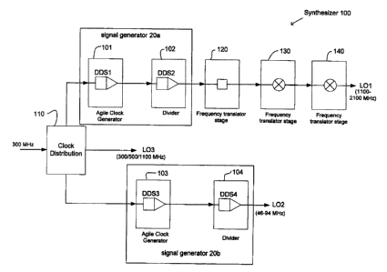
[0026] FIGURE 1 is a block diagram of a frequency synthesizer 100
according to at least one embodiment;
[0027] FIGURE 2 is a detailed block diagram describing the clock
generator in at least one embodiment;
[0028] FIGURE 3 is a detailed block diagram describing the clock
divider in at least one embodiment;
[0029] FIGURE 3a is a detailed block diagram of another embodiment
of the clock divider and a frequency multiplier;
(0030] FIGURE 4 is a detailed block diagram of an embodiment of the
first synthesizer stage;
[0031] FIGURE 5 is a detailed block diagram of an embodiment of the
second synthesizer stage;
[0032] FIGURE 6 illustrates an embodiment of a synthesizer including
a clock generator coupled to more than one divider;
[0033) FIGURE 7A is a block diagram of another embodiment of a
synthesizer;
[0034] FIGURE 7B is a block diagram of another embodiment of a
synthesizer;
CA 02491119 2004-12-23
9
[0035] FIGURE 8a is a block diagram of an embodimcnt of a
programmable divider chip;
[0036] FIGURE 8b is another block diagram of an embodiment of a
programmable divider chip;
[0037] FIGURE 9 is a block diagram of a fast tuning, high spectral
purity tuner/receiver according to an embodiment;
[0038] FIGURE 14 is a block diagram of a DDS chip/chipsets
according to an embodiment;
[0039] FIGURE 11 is an illustrative information flow diagram for a
test and measurement signal generator/spcctnun analyzer front end according
to an embodiment;
[0040] FIGURE 11A shows a block diagram of a signal analyzer
according to an embodiment of the invention;
[0041] FIGURE 11B shows a flowchart of a method of signal analysis
according to an embodiment of the invention;
[0042] FIGURE 11 C shows a flowchart of a method of signal analysis
according to another embodiment of the invention;
[0043] FIGURE 11D shows a block diagram of a signal analyzer
according to another embodiment of the invention;
[0044] FIGURE 11 E shows a flowchart of a method of signal analysis
according to another embodiment of the invention;
[0045] FIGURE 1 IF shows a block diagram of an implementation of a
signal analyzer as shown in FIGURE 11 D;
CA 02491119 2004-12-23
[0046] FIGURE 12 is a block diagram of a secure transceiver having a
modulation scheme provided in accordance with an embodiment;
[0047] FIGURE 13 is a block diagram of a satellite communication
system in accordance with an embodiment;
[0048] FIGURE 14 is a series of scatter plot diagrams showing
examples of the effects of improved phase noise in an embodiment;
[0049] FIGURE 15 is an overall block diagram of a radar system
according to an embodiment;
[0050] FIGURE 16 is a block diagram of at least one embodiment of
divider having a variable frequency input source;
[0051] FIGURE 17 is a flow diagram of a method according to at least
one embodiment;
[0052] FIGURE 18 shows a theoretical plot of the output signal
produced by at least one embodiment having a divide ratio of 2.990;
[0053] FIGURE 19 shows a theoretical plot of the output signal
produced by at least one embodiment having a divide ratio of 2.999;
[0054] FIGURE 20 shows a theoretical plot of the output signal
produced by at least one embodiment having a divide ratio of 3.000;
[0055] FIGURE 21 shows a theoretical plot of the output signal
produced by at least one embodiment having a divide ratio of 2.5000;
[0056] FIGURE 22 shows a theoretical plot of the output signal
produced by at least one embodiment having a divide ratio of 3.1000;
[0057] FIGURE 23 shows a theoretical plot of the output signal
produced by at least one embodiment having a divide ratio of 6.1991;
CA 02491119 2004-12-23
11
[0058] FIGURE 24 shows a block diagram of a signal generator 10
according to an embodiment of the invention;
[0059] FIGURE 25 shows a block diagram of a DDS having a divide
ratio of 2;
[0060] FIGURE 26 shows a block diagram of a DDS having a divide
ratio of 2.5;
[0061] FIGURE 27 shows a flowchart of a method according to an
embodiment of the invention; and
[00b2] FIGURE 28 shows a flowchart of a method according to an
embodiment of the invention.
DETAILED DESCRIPTION
[0063] Unless indicated otherwise, the terms "signal generator,"
"synthesizer," and "frequency synthesizer" are used interchangeably herein.
Embodiments described as "exemplary" indicata illustrative examples only
and are not necessarily preferable over any other embodiment.
[0064] Embodiments of the present invention may include a
symhesizer architecture suitable for signal generation, for example, in
wideband applications. In at Toast one embodiment, the DDS synthesizer
includes a clock generator configured to provide a tunable or varying clock
input to one or more other DDSs. Operation of such a device may include
selecting the output frequency of the clock generator (which may also include
a DDS) to reduce or prevent spurious components in the output of a
subsequent DDS or DDSs. Such embodiments may be applied, for example,
to produce signals over a wide frequency range.
CA 02491119 2004-12-23
12
[0065] FIGURE 24 shows a block diagram of a signal generator 10
according to an embodiment of the invention. Clock generator 101, which
may include one or more DDSs, generates a synthesized clock signal based on
a clock source signal (not shown). Divider 105, which may also include one
or more DDSs, receives the synthesized clock signal (or a signal based on it)
and generates a divided signal based on the synthesized clock signal and a
ratio. A bank 167 of selectable filters receives the divided signal (or a
signal
based on it) and a selected one of the filters is applied to filter the signal
to
produce an output. The selection among the selectable filters is based on the
ratio. Further embodiments of signal generator 10 as described herein may
include components such as filters, frequency translators, switches, and/or
summers in the signal paths between clock generator 101 and divider 105,
between divider 105 and selectable filters 167, and/or downstream of one or
more of selectable filters 167.
[0066] FIGURE 1 shows a fimctional block diagram of an synthesizer
I00 that includes two implementations 20a,b of signal generator 10.
Synthesizer 100 may be configured as a wideband Local oscillator signal
generator, for example, to include a first agile clock generator 101
configured
to provide a first clock signal. In this implementation, clock generator 101
receives a first clock source signal (and possibly other signals) from a clock
distribution unit I 10. For example, clock distribution unit 110 may generate
or receive a 300 MHz clock signal input and output a 300 MHz clock signal
based on that signal to the clock generator 101. In another implementation,
clock generator 101 may include an oscillator configured to generate the first
clock signal or a precursor of such signal. Such an oscillator may be a
crystal
oscillator (e.g. a temperature-controlled crystal oscillator or TCXO) or other
suitable device.
[0067] In at least one embodiment, the clock generator 101 produces a
DDS clock signal input to a clock divider I02. Clock generator 1 O1 may
CA 02491119 2004-12-23
13
include a step recovery diode (SRD) and associated circuitry for clock
generation (e.g. by multiplying a clock signal having a lower frequency).
Clock divider 102 may be configured to output a divided signal based on the
DDS clack signal input and the state of a control word.
[0068) FIGURES 2 and 3 provide additional details concerning
possible implementations of clock generator 101 and clock divider 102,
respectively. As shown in FIGURE 2, clock generator 101 may include a
DDS 151 coupled to a variable bandpass (and/or switched bandpass) filter
153, the output of which may be provided to a frequency translator l 55. The
variable bandpass filter 153 may remove artifacts due to the clock signal as
well as other artifacts such as alias and spurious responses.
[0069) The ternr "frequency translator" as used herein includes devices
such as frequency multipliers (e.g. circuits including SRDs) and mixers.
Frequency translator 155 may be implemented as a mixer to receive a first
local oscillator signal and produce an upconverted output DDS clock signal.
In at least one implementation, the first local oscillator signal is derived
from
the same base as the clock signal provided by the clock distribution unit I 10
to
the DDS 1 S 1 and may even be the same signal. Furthermore, the output DDS
clock signal may be implemented as a sine wave that is continuously tunable
across a range (for example, to any frequency across the output band of the
DDS 151 ). The output DDS clock signal may be filtered using one of multiple
selectable bandpass filters (or switched bandpass filters, or a singular
filter)
157 to produce a filtered output DDS clock signal.
[0070] As shown in FIGURE 3, clock divider 102 may include a DDS
161 that receives the output DDS clock signal from clock generator 101. The
DDS 161 may product a divided signal which is provided to a variable
bandpass (or switched bandpass, or singular) filter 163 coupled to an output
of
DDS 161. The variable bandpass filter 163 may remove artifacts due to the
CA 02491119 2004-12-23
I4
clock signal as well as other artifacts such as alias and spurious responses.
The divided signal output by the DDS 161 may be, for example, a sine wave
that is tunable over a broad frequency range.
[0071] The filtered divided signal may then be provided to a frequency
translator 165 configured to produce a translated divided signal (e.g. by
mixing the filtered divided signal with a second local oscillator signal). The
translated (e.g. upconverted) divided signal may be filtered using one of
multiple selectable bandpass filters 167 to produce a filtered upconverted
divided signal. In at least one embodiment, the DDS 16I selects the particular
bandpass filter 167 based on the state of the control word.
[0072] In some embodiments, the divided signal output by the clock
divider 102 has a frequency at least two times but less than three times lower
than the DDS clock signal received from the clock generator 101. In at least
one embodiment, the divided signal has a frequency that is 2.5 times Iower
than the DDS clock signal. In such embodiments, it may be sufficient to
provide filtering of the output only to suppress the images appearing at 0.5
and
1.5 times the output frequency. Thus, the only dividing restriction nearing an
integer value of 2 is the restriction imposed by the sampling nature of the
digital architecture, which may cause images to be abased back into the
bandwidth of interest.
[00'f3] In at least one embodiment, four has been found to be a suitable
number for the set of selectable bandpass filters 157 and 167, each of which
is
individually selected for filtering its respective input signal. In at least
one
embodiment, each of the filters of the set of filters 157 and 167 may be
constructed using discrete components, which may be separate components for
each filter. Alternatively, four has been found to be a suitable number for
the
set of selectable bandpass filters 153 and 1 b3, if selectable input
frequencies to
the agile clock generator are used. Use of selectable input frequencies to the
CA 02491119 2004-12-23
agile clock generator 101 may be further advantageous in increasing the spurs-
free bandwidth of the output of the clock generator 101.
[0074] E~h of the filters comprising the set of filters 1 S7 and 167, as
well as any other set of selectable bandpass filters herein, may have a
different
bandpass frequency range as well as a smaller or larger relative bandpass
range (i.e., the size of the filter's range calculated as the difference
between
the high frequency cutoff and the low frequency cutoff for the filter)
compared
to other filters in the set. Depending on the requirements and/or tolerances
of
the particular application or design, adjacent passbands may overlap or be
nonoverlapping. One possible arrangements for the passbands of the filters in
a set is as a series of octaves.
(0075] For example, filter set 1 S7 may have four filters and be
implemented to pass the band SU-200 Ml~fz. If the individual filters were
implemented to have passbands of equal width, then the respective passbands
might be centered at 50,100,150, and 200 MHz, each filter passing a band
+/- 25 MHz from the center frequency. Such a distribution would not be
suitable for removing images at O.Sx and l.Sx from an output frequency of SO
MHz, however, as the 2S MHz and 7S MHz images would lie within (or at
least at the edge ofj the passband of the SO-MHz filter. Therefore, another
distribution of the center frequencies and/or passbands of the filters might
be
more desirable. For example, the same center frequencies may be used, with
the filters having progressively wider passbands as the center frequency
increases. Alternatively, the filters may have center frequencies that are non-
unifonnly distributed. For example, an octave or semi-octave distribution
(e.g. 50-70-100-140) may be used instead, with each filter having a passband
slightly more narrow than the center frequency.
[0076] The DDSs 1 S 1 and 161 may receive one or more control words
which cause the DDSs to produce output signals having particular frequencies
..~..-
CA 02491119 2004-12-23
16
and phases. For example, the control words may include digital phase and
frequency information. The control words may be stored by the DDSs 151
and I61 in, e.g., an accumulator or other such register for decoding and
processing.
[0077] In at least one embodiment, an accumulator of a DDS used in
the embodiment (e.g. DDS 151 or 161) may add the digital information
contained in the received control words to the binary value already in the
accumulator (e.g. using modulo-2 addition) to form a new iiequencylphase
index value. The DDS may then use the newly formed frequency/phase index
value to determine from a phase lookup table the frequency and phase of the
signal to output from the DDS.
[0078] In particular, in at least one embodiment one or both DDSs is
phase continuous. That is, the DDS accumulates from the current value in the
phase accumulator when a new accumulator value is written to the
accumulator. When a new frequency value (phase accumulator value) is
written, it accumulates or adds to the last value in the accumulator unless
the
DDS is purposely re8et to a phase accumulator value of zero.
[0079] In an embodiment, the clock divider 102 may be preloaded to
output the divided signal at a predefined frequency in response to receiving
the
DDS clock signal input.
(0880] The following Table 1 provides a particular example of
frequency planning, including control information that may be used to control
particular implementations of DDSs 151 ("DDS 1 ") and 161 ("DDS2") to
perform signal synthesis operations as described herein. In at least one
embodiment, control logic is used to control the functioning of the DDSs 151
and 161 to produce particular divided signals according to Table 1. For
example, one or more such control words may be loaded into a control register
of a DDS. This logic may be implemented using, for example, a gate-based
CA 02491119 2004-12-23
I7
logic design embodied in a Field Programmable Gate Array (FPGA), an
Application Specific integrated Circuit (ASIC), a series of discrete
components, and/or processor-executable instructions stored in a memory
{which may be a Read-Only Memory {ROM), Programmable ROM {PROM),
Erasable PROM (EPROM), nonvolatile random-access memory (NVRAM),
flash memory, or any variation thereof).
[0081] In this example, the output of DDS 1 151 is upconverted by 300
MHz before input to DDS2161. The DDS2 161 applies a selected divide
ratio, and its output signal may be doubled to obtain the desired output
signal.
Given a selected output frequency, a known range of acceptable divide ratios,
and a known set of available upconversion options, control logic may be
implemented to select the appropriate output frequency for DDS 1 151:
DDS1 DDSl OUT (MHz)DDS2 DDS2 DDS2 FREQ
RANGE DIVIDE OUT DOUBLED OUT
RATIO ?
50 - DS2 * 3. - 3.5 100-I09 NO 100-109
81.5 300
27 - DS2 * 3.0 - 3.0 109-131 NO 109-13I
93 300
27.5 DS2 * 2. - 2.5 131-150 NO 131-150
- 75 300
75 - DS2 * 5.0 - 5.0 75-78 YES 150-156
90 300
51- 69 DS2 * 4.5 - 4.5 78-82 YES 156-164
300
28 - DS2 * 4.0 - 4.0 82-98 YES 164-19b
92 300
43 - DS2 * 3.5 - 3.5 98-109 YES 196-218
81.5 300
27 - DS2 * 3.0 - 3.0 109-131 YES 218-262
93 3
00
27.5 _ _ _ YES 262-300
- 75 {DDS2 * 2.5) 2.5 131-150
- 300 ~ ~
TABLE 1. DDSI & DDSZ CONTROL
[0082] In at least one embodiment, the clock divider 102 includes a
look-up table of amplitude values that may be used to directly specify the
divided signal output (e.g. without converting phase values). In response to
the control word, for example, the outputted value may be determined based
on the table of amplitude values. In at least one embodiment, the clock
divider
CA 02491119 2004-12-23
18
102 outputs new values of the divided signal at a frequency substantially
equal
to the frequency of the DDS clock signal without the full phase-to-amplitude
conversion. The lookup table of DDS 151 for the clock generator 101 may
also contain entries previously determined to rcduce or prevent the generation
of spurious components in the frequency spectrum of the DDS clock signal
produced by the clock generator 101.
[0083] In at least one embodiment, spurious content is reduced by
tuning the Divider DDS to integer or integer +/- O.X values, where X is a
digit.
In particular, X may be equal to 5. However, other values for X are possible
(e.g. 1). Alternatively, X may be a real number. This selection may have the
effect of causing the spurious responses (e.g. images as generated by DAC
errors such as quantization and non-linearity) to be masked under the
fundamental frequency (output frequency). For exact integer divide values, all
spurious content due to DAC error may fall under the fundamental frequency.
For integer values +/- O.X, some spurious content may fall undcr the
fundamental, with the closest remaining spurious content falling at a
frequency equal to the output frequency +/- (0.X * output frequency). It is
then possible to determine the number of filters and their rejection needs
based
on the spur-free ranges of the output frequency.
[0084] FIGURE 3a shows a further embodiment of clock divider 102
and frequency translator stage 120. As shown in this figure, the clock divider
102 may include a DDS 161 that receives the clock signal output by the clock
generator 101. The DDS 161 may produce a divided signal which is filtered
using one of multiple selectable bandpass filters 167 to produce a f ltered
divided signal. In at least one embodiment, the DDS 161 may select the
particular bandpass filter 167 based on the state of the control word. Fox
example, the divided signal output by the DDS 161 may be a sine wave
tunable over a broad frequency range.
CA 02491119 2004-12-23
19
[0085] The filtered divided signal may then be provided through a
driver 169 to a frequency translator stage 120 where the filtered divided
signal
is iranstated to produce a translated divided signal. Frequency translator 121
may be implemented as a multiplier, for example, using a comb generator
including a snap or step recovery diode. Alternatively, frequency translator
121 may include a mixer configured as a frequency doubter (or "dedicated
multiplier"), with the input signal being coupled to both of the RF and LO
inputs of the mixer.
[008b] The translated divided signal may be filtered using one of
multiple selectable bandpass filters I23 to produce a filtered translated
divided
signal. For example, the number of selectable bandpass filters may be four.
In at least one embodiment, the DDS lbl may select the particular bandpass
fitter 123 based on the state of the control word. The filtered translated
divided signal may then be provided thmugh a driver 125 (e.g. a buffer,
amplifier, or impedance-matching network) to one or more frequency
translators to produce other frequencies of interest.
(0087] FIGURE 4 shows a detailed functional block diagram of an
embodiment of frequency translator stage 130. As shown in this figure, the
frequency translator stage 130 that outputs a first portion of the first local
oscillator signal may include a frequency translator i 31 (which may be
coupled to the frequency translator stage 120), the output of which is coupled
through switches 132 and 135 to one or more selectable bandpass filters 133
and 134. In at least one embodiment, the frequency translator stage 130
selects the bandpass filter 133 or 134 based on the frequency of the received
filtered translated divided signal. In an embodiment, the number of selectable
bandpass filters in this stage is two, although more or fewer filters may be
used as appropriate.
CA 02491119 2004-12-23
[0088] The bandpass filters 133 and 134 are selected based on the
desired output frequency of the stage or an intermediate frequency needed to
perforna a conversion to the desired output frequency. For example, in a
particular implementation as shown in FIGURE 4, either the 1100-1300MHz
bandpass filter 133 or the 1300-1500MHz bandpass filter 134 is selected based
on the desired output frequency for the first frequency translator stage 130,
which ranges from 1100 MHz to 1500 MHz. As shown in FIGURE 4, an
intermediate frequency (IF) input of 100-300MHz from the preceding stage
I20 may be mixed with either 1000MHz or 1200MHz to produce the above
stated output.
[0089] In at least one embodiment, control logic may be used to select
the filter 133 or I34 based on the desired output frequency. The control logic
may be implemented using, for example, but not limited to, an FPGA, ASIC,
ROM device, or software, as described above. The control logic may first
determine the output frequency to be provided, and then determine the local
oscillator frequency needed to upconvert to the final output. In an
embodiment, if the desired output frequency is between 1100-1300MHz, then
the 1000MHz local oscillator signal is selected and mixed with 100-300MHz
using the frequency translator 131 to yield I 100-1300MHz, as shown in
FIGURE 4. On the other hand, if the desired output frequency is from >1300-
1500MHz, then the 1200MHz local oscillator signal is selected and the 1300-
1500MHz filter 134 is selected. In at least one embodiment, selecting the LO
signal and the filter may be accomplished with the same control signal.
Additional details regarding the control logic and control flow are described
herein with respect to FIGURE 16.
[0090] FIGURE 5 shows a detailed functional block diagram of an
embodiment of frequency translator stage 140. As shown in this figure,
frequency translator stage 140 may include a pair of switches 144 and 145
which, in a first position, configures the frequency translator stage 140 to
CA 02491119 2004-12-23
21
provide the received signal to a frequency translator 141 (e.g. a mixer) which
may be coupled to one of multiple selectable bandpass filters 142 to produce a
filtered signal. In at least one embodiment, the frequency translator stage
140
may select the particular bandpass filter 142 based on the final output
frequency required at the output of the frequency translator stage 140. In a
second position, the switches 144 and 145 configure the frequency translator
stage 140 to output the signal received by the stage. In either case, the
second
stage signal through switch 145 is provided through the driver 146 as the
first
local oscillator final output signal. In the particular implementation shown
in
FIGURES 1 and 5, the first local oscillator signal output by this stage has a
frequency of between I I 00 MHz and 2100 MHz.
[0091] In at least one embodiment, the switch settings for filtering and
upconversion selection or bypass are selected by control logic based on a
stage
output frequency, the desired final output frequency of the first local
oscillator
LOI {e.g., 1100--2100MHz), or an intermediate frequency used for
upconversion to produce one of these. A filter may be selected that has a
passband within the range of the output frequency and that attenuates the
unwanted terms, such as the local oscillator input in the upconversion case.
If
the stage 140 is not configured for upconversion (e.g., the output frequency
is
between 1100-I SOOMHz), then the translator 141 is bypassed and the output
frequency from the previous stage (e.g., frequency translator stage 130 in
FIGURE 4) is used.
(0092] In at least one embodiment as illustrated in FIGURE 1, the
synthesizer 100 may further include a second signal generator (i.e. a second
clock generator 103 coupled to a second divider i 04) configured to produce a
second local oscillator signal. The clock signal received from the clock
distribution unit 1 I0 by the second clock generator 103 may have the same
frequency as the clock signal received by the first clock generator 101;
alternatively, clock distribution unit 110 may provide a signal having a
CA 02491119 2004-12-23
22
different frequency to generator 103. The structure and operation of the
second clock generator 103 and the second divider 144 may be substantially
the same as described above for the first clock generator 101 and the first
divider 102 in FIGURES 1-3a. The second local oscillator signal may have,
for example, a frequency between 48 MHz and 94 MHz. In order to generate
higher local oscillator frequencies, the output of the second divider 104 may
be coupled to an upconverter and/or one or more synthesizer stages as
described above.
[0093] In at least one embodiment, the synthesizer 100 may provide a
third local oscillator signal. The third local oscillator signal may have, for
example, a frequency of one of 300 MHz, 500 MHz or 1100 MHz. In an
embodiment, the clock distribution unit 110 may include one or more step
recovery diodes (SRDs) configured to generate the third local oscillator
signal.
(0094] Alternatively, a varying tunable clock source may be
. constructed using other than DDS methods and devices to provide the clock
for the second or subsequent DDS(s). An example of such a varying, tunable
clock source is a phase-locked loop. While a phase-locked loop may be
slower to tune, such a device may provide tower power consumption (down to
milliwatts) and/or a smaller size (due e.g. to reduced filtering requirements)
in
comparison to a DDS. In such embodiments, the variable-frequency clock
signal is received by the clock divider(s), which may be as described earlier
with respect to FIGURES 1-3a.
[0095] In a further embodiment, a synthesizer 200 may include a clack
generator 201 coupled to more than one divider (for example, dividers 202-
204 as shown in FIGURE 6). In at least one embodiment, one or more of
dividers 202-204 are implemented using DDSs. Multiple clock dividers may
be used, for example, to reduce or eliminate the time it takes to load a new
division ratio or control word into a DDS divider. In one implementation, one
CA 02491119 2004-12-23
23
or more of the clock dividers 202-204 are preconfigured (i.e. before being
selected into the signal path) with a particular division ratio, control word,
and/or output frequency/phase in order to achieve even faster switching time.
In an exemplary application, such an architecture may be used to "ping-pong"
between or "hop" among different frequencies very rapidly.
[0096] For example, one or more of clock dividers 202-204 may
include multiple registers for preloading of different pre-defined divider
values, with the divider capable of selecting one of the preloaded divider
values in response to a signal provided by control logic external to the
divider
at a rate faster than the time required to load each divider individually. The
control signal may be provided upon or prior to the divider being selected
into
the signal path.
(0097] Alternatively, each of the multiple dividers 202-204 may be
preconfigured or preloaded with a single respective divider value, and then
each divider may be individually selected (e.g. by switch 205) at a rate
faster
than the time required to load each divider individually, in order to achieve
a
very fast tuning speed. In at least one embodiment, the dividers 202-204 may
have a parallel loading control word register {as opposed to a register that
is
loaded serially).
[0098] It should be noted that although FIGURE b shows three
dividers 202-204, any number of dividers or divider DDSs may be used in
various embodiments. The architecture may also be implemented to include a
switch between the clock generator 201 and the dividers 202-204.
[0099] In an alternative implementation, a divider chip may have
multiple (e.g. four or eight) different pin-selectable profiles, each
including its
own control word or divide ratio, such that fast frequency switching may be
achieved during operation, as described above with respect to FIGURE 6. In
one such implementation, such a divider chip may provide phase-continuous
CA 02491119 2004-12-23
24
switching between two different frequencies. Alternatively, the architecture
of
FIGURE 6 may be implemented using a summer in place of (or in addition to)
switch 205, such that outputs from multiple dividers (e.g. 202 204) may be
combined to provide a modulated output signal or a desired waveform shape.
[OOi00] Furthermore, alternatively at least one of the dividers
202-204 may be a non-DDS based frequency divider. For example, such a
frequency divider may be constructed as or including a logic chip (e.g. TTL,
ECL) or using discrete components, or may otherwise include an integrated
circuit capable of outputting a divided frequency. Alternatively, such a
divider may produce a divided signal according to one of several different
divide ratios in response to a selection signal. Such embodiments may offer a
reduced set of available divide ratios, such that the clock generator 201 may
be
required is certain applications to have a frequency range that is greater
than
embodiments in which at least one of the dividers 202-204 is implemented
using a DDS.
[00101] As shown in FIGURE 7A, a synthesizer 700 according
to another embodiment may include a clock generator 701 coupled to a first
divider stage 710, the output of which is in turn coupled to a second divider
stage 703. In such embodiments, at least one or all of the clock generator
701,
first divider stage 710, and second divider stage 703 may be implemented
using DDSs: For example the clock generator 701 may comprise a first DDS,
which may be coupled to a second DDS implementing first divider stage 710,
which may be coupled to a third DDS implementing second divider stage 703.
The third DDS or second stage divider may, for example, substantially
replicate the second DDS or divider in the embodiments described above.
[00102] Advantages of using a third DDS serially coupled to the
output of the second DDS may include finer tuning resolution (e.g., micro-
hertz resolution) and/or further spurious component suppression,
CA 02491119 2004-12-23
Furthermore, a first DDS (c.g., agile clock or clock generator DDS) having
increased tuning resolution but reduced spurious performance may be used. In
such embodiments, the spurious components produced by the first DDS (e.g.,
agile clock generator DDS) may be reduced by, for example, 20 log [(second
DDS divide value) x (third DDS divide value)). Thus, the addition of a third
DDS may further reduce spurious responses created by the first DDS (e.g.
agile clock generator) while providing finer tuning resolution. As in other
embodiments, one or more of the DDSs may be preloaded for rapid frequency
switching. Furthermore, as shown in FIGURE 7B, a first divider stage 722
may be implemented to include more than one divider, such as the dividers
710 and 711. Such dividers may have outputs that are selectable (e.g. via
switch 712) or combinable (e.g. to obtain modulated signals or other
waveforms).
[00103] Regarding the clock divider 102, in at least one
embodiment the DDS 161 may include a table of amplitude values to be
output directly to a DAC at the rate of the input clock. Such an architecture
bypasses the phase-to-amplitude conversion of current DDS architectures and
may thus eliminate the need for a control word input. The table of amplitude
values may be small (i.e., implemented only for integer or integer +/- 0.5
ratios), such that the control word may be replaced by a signal to specify the
integer (+I-0.5) ratio to be applied. In particular, such an embodiment may
use
ratios such as, for example, integer values +I- 0.5 and/or integer values +I-
.1,.2,.3 or .4. Other acceptable solutions may include non-integer ratios of
the
divider DDS that have been found to provide wide bands free of spurious
responses (e.g., as shown in FIGURE 23). This approach is flexible to
respond to particular requirements such as application bandwidth, spurious-
free dynamic range, size requirements, etc.
[00104) In an embodiment, the synthesizers described above
may be implemented using an integrated circuit device as a programmable
CA 02491119 2004-12-23
26
divider chip DDS for use in signal generation. The chip may be programmed
by sending it a particular divide ratio indicative of a corresponding sine or
cosine value to use for each clock cycle. The output may be a sine wave;
however, other waveforms are possible. Such a programmable divider chip
may be designed for particular applications, such as, for example,
applications
that may use dual DDS configurations, and therefore utilize a simplified or
streamlined design. In the case of the Dual DDS Synthesizer, one DDS may
be used to clock a second DDS operable to fimetion with only specific divide
ratios for particular spectral purity concerns.
[00105] As discussed above, dual DDS synthesizers may be
implemented to have the advantage of reducing spurs. Spurious responses is
one characteristic of previous DDS architectures that has limited the
widespread use of DDSs, particularly for wideband applications. At
predictable intervals of the clock as it relates to the tuned output
frequencies,
the DDS has many close-in spurious responses. In narrowband systems, the
clock is set at a single frequency to avoid these close-in responses, but this
also limits the tuning range. Consequently, these spurious responses may
prohibit the use of existing DDS architectures in wideband systems.
[00106] In at Least one embodiment of the present invention, the
first DDS provides a tunable clock for the second DDS, which allows the input
clock to the second DDS to be tuned as necessary to mitigate the inherent
spurious regions of the second DDS. This configuration eliminates and/or
significantly reduces close-in spurious responses to utilize the desired
benefits
of the DDS, which include excellent phase noise and fast tuning speed.
Because the cleanest output spectrum is obtained at integer and half integer
ratios, a DDS chip dedicated to these division ratios may be optimized for
that
function.
CA 02491119 2004-12-23
27
[00107] A further embodiment of the invention includes a
programmable divider chip. Such a DDS synthesizer chip configured
specifically as a divider DDS may be utilized in a variety of wideband
applications where fast tuning and low phasa noise characteristics are
desired.
These applications are not limited to but may include signal surveillance,
electronic warfare, test equipment, transmitters, radar and data
communications. Particular advantages of a divider DDS (as compared to,
e.g., analog designs) may include simpler design, faster design, smaller
tuning
word, lower spurious responses, higher fidelity and lower phase fitter.
(00108] As shown in FIGURE 8a, a programmable divider chip
according to an embodiment of the invention may include three sections: a
divide-ratio-to-table-address mapping section 801, a lookup table (e.g. sine
and/or cosine) 802, and a digital-to-analog converter (DAC) section 803. The
divide-nriio-to-address mapping section 801, which outputs a sequerxe of
addresses for lookup table 802 according to an indicated divide ratio, may be
implemented in several different ways, with selected divide ratios (e.g. all
or
part of the series of 2.5, 3, 3.5, 4, 4.5, . ..,100) being supported. In the
case of
divide by 4, for example, mapping section 801 may indicate the address in
lookup table 802 for the sine or cosine value for every 90° (or
0°, 90°,180°
and 270°), to be output to DAC 803, at a rate of one address/angle for
every
clock cycle. Thus one complete cycle of the divide by four output may be
produced in four clock cycles. In the case of divide by 2.5, mapping section
801 may indicate the address for the sine value for 0°,144°,
288°, 432°, and
S76°, to be output to DAC 803 at the same rate. In this case, two
complete
cycles of the divide by 2.5 output may be produced in five clock cycles.
Operations for other divide ratios may be inferred from this logic. Such a
chip
may also include selectable (e.g. pin-selectable) profiles as described
herein.
[00109] Such embodiments ntay provide a sine or cosine wave
output; however, other embodiments of this basic structure are possible. One
CA 02491119 2004-12-23
28
example, as shown in FIGURE 8b, may include having the divide ratio to
ROM lookup as one function 804. Another example is a lookup table based
on a non-sinusoidal waveform (e.g. a triangle, sawtooth, or other waveforms).
[00110] Table 2 below lists some examples of incremental phase
values that may be used to produce certain divider ratios.
Divider Phase Increment
Ratio (Degrees)
13 27.89230769
12.5 28.8
12 30
_ _
11.5 31.30434783
11 32.72727273
10.5 34.28571429
36
9.5 37.89473684
9 40
8.5 42.35294118
8 45
7.5 48
7 51.42857143
6.6 65.38A61538
6 60
5.5 65.45454545
5 72
4.5 80
4 90
3.5 102.8571429
3 120
~2.5
Table 2
[00111) As may ~ realized by reviewing the phase increment
numbers, many values may be reused. For example, divide by 12 would have
12 values every 30 degrees and would encompass all 6 values of a divide by 6
which would have values every 60 degrees. A reuse of such numbers, and
CA 02491119 2004-12-23
29
resultant reduction of the size of the lookup, allows simplification of the
DDS
to be realized in implementation.
[00112] Use of a DDS at a divide ratio of 2 (i.e. the Nyquist
frequency) is not currently known. One possible reason is that a DDS may
exhibit a decrease in output signal strength of up to 20 dB or more at an
integer ratio of 2 as compared to output signal strength at higher divide
ratios.
[00113] Some DDSs, such as a DDS in the Analog Devices
series 98XX, include a provision for adding a phase offset value to the phase
value that is output by the phase accumulator (e.g. before digital-to-analog
conversion). The inventors have discovered that by selecting a phase offset of
90 degrees (or 270 degrees), an output signal strength may be achieved at an
integer ratio of 2 that is comparable to results at higher divide ratios (see,
e.g.,
FIG. 25).
[00114] Such a technique may be used to particular advantage
with a DDS driven by a variable-frequency clock {e.g. a PLL or another DDS),
as described herein. In one such application, the divider DDS is configured
with a divide ratio of 2 and a phase offset of 90 degrees. The clocking PLL or
DDS may be used to provide frequency variability and/or wideband operation,
while the divider DDS may be used to provide a phase-continuous and/or
relatively spurious-free output at half of the clocking frequency. It may be
determined that a different phase offset value provides similar advantages
with
other DDS models.
(00115] Adjustment of a phase offset value of a DDS may also be
used in conjunction with divide ratios of X.S, where X is an integer greater
than or equal to 2 {see, e.g., FIG. 26). In a method according to another
embodiment of the invention, a phase offset value is selected to provide
decreased spurious signal strength and/or increased output signal strength.
CA 02491119 2004-12-23
3Q
(00116] As mentioned above, DAC nonlinearity may give rise to
spurious content. DAC nonlinearities are typically greater at higher
frequencies. One reason for this effect may be that outputs at lower divide
ratios are converted using fewer data points than outputs at higher divide
ratios. Possibly because of this effect, operation of a DDS at a divide ratio
of
2.5 is currently unknown. Filtering and other techniques that may be used to
enable such operation are described herein.
[00117) As noted herein, a DDS operated at a divide ratio of X.5
(where X is an integer greater than or equal to 2) may be expected to have
spurious outputs at 0.5 and 1.5 times the output frequency (see, e.g., FIG.
21).
Hy changing or selecting a phase offset value of the DDS, the strength of one
or both of these spurs may be reduced.
[00118] Such a method may be further applied, e.g., to simplify a
filtering task. For example, a filter may reduce the strength of a spur
resulting
from one clock frequency, but may not have a sufficient effect on the strength
of a spur resulting from another clock frequency to meet a particular design
specification. By reducing the strength of the spur as described above in at
least the second case, it may be possible to meet the specification by using
the
same filter in that case, which may avoid a need to add another filter to the
system. A method as described herein may also be used with a DDS operated
at a divide ratio other than X.S.
[00119] In a case where a phase offset value is changed or selected for
a DDS to be operated at a divide ratio of X.5 (where X is an integer greater
than or equal to 2), it may be possible that a suitable phase offset value
(i.e. a
value that results in a desired or acceptable reduction of spur strength
and/or a
desired or acceptable increase in desired signal strength) will change over
time. For example, such a value may change based on effects of temperature,
capacitance, frequency, device aging, etc. Therefore, it may be desirable to
CA 02491119 2004-12-23
31
monitor a strength of one or more spurious components of the output signal of
a DDS, and to change or select a phase offset value of the DDS based on a
result of the monitoring (see, e.g., FIG. 27). Such a method may also be used
with a DDS operated at a divide ratio other than X.S. Additionally, such a
method may be used to increase a strength of the desired signal, either with
or
without reducing a strength of a spur.
[00120] It may be possible to obtain information from one or more
DDSs that may be used to change or select a phase of~'sct value to produce a
desired output for a different DDS of the same model number, a different
DDSs from the same batch, etc. at least with respect to operation at the same
frequency, at the same divide ratio, and or in the same application. For
example, it is possible that an optimum or otherwise desirable phase offset
value may depend on one or more particular propagation paths (which may be
internal and/or external to the DDS), and that information regarding a
relation
between the value and the paths) may be obtained and applied to the use of
other DDSs. For example, it may be possible to use information relating to
measurements at two or more different clock andlor output frequencies to
calculate a phase offset value having advantages at another frequency (see,
e.g., FIG. 28). Particular methods of characterization, interpolation, etc. as
are
known in the art may be applied in a method according to such an embodiment
of the invention.
[00121) As the description herein demonstrates, embodiments of the
present invention may be used for applications where one or more ultra-clean,
fast tuning frequency sources are desired. Examples include, but are not
limited to, a Local oscillator in frequency conversion, complex modulation,
and
transmission and test & measurement applications. In general, the present
invention may also be used for applications previously implementing a phase
locked loop (PLL). Particular applications are described below with respect to
FIGURES 9-16.
CA 02491119 2004-12-23
32
~ooizz~ FIGURE 9 is a block diagram of a fast tuning, high spectral
purity tuner/receiver 900 according to an embodiment. In particular, FIGURE
9 illustrates an embodiment of a tuner/receiver designed for fast tuning speed
and high spectral purity (phase noise and spur free dynamic range {SFDR)).
Applications for such an embodiment may include Signal Intelligence
(SIGiNT) and Electronic Intelligence (FLINT) signal collection and analysis.
In at least one embodiment, the receiver/rimer 900 may include a radio
frequency (RF) antenna 901 coupled to a receive band filter 903, the output of
which is fed through a low noise amplifier 905 to a first frequency translator
907 to produce a first intenmediate frequency (1F,). The output of frequency
translator 907 is coupled through a bandpass filter 909 to a second frequency
translator 911 that produces a second IF (IFz). The output of the second
frequency translator 911 may be fed through a bandpass filter 913 and an
amplifier or signal conditioner 915 to a third frequency translator 917 to
recover the detected digital signal. The output of frequency translator 917
may be coupled through a first low pass filter 919, an amplifierlsignal
conditioner 921, and a second low pass filter 923 to a DAC 925 to reconstruct
the analog signal corresponding to the detected digital signal. In such
embodiments, the tuning speed and spectral purity of a receiver may be
determined by its synthesizer (LO1, L02, and L03 inputs to frequency
translators 907, 909 and 917, respectively, in the particular implementation
shown in FIGURE 9). The phase noise, SFDR and tuning speed of
embodiments of the present invention are well-suited for such applications. In
particular, any one or all of LO1, L02 and L03 may be implemented using
embodiments of a signal generator or synthesizer as described herein (e.g.
including one or more implementations of signal generator 10). Alternatively,
one or both of L02 and L03 may be implemented using other solutions such
as PLL-based or SRD-based signal generators.
,.....
CA 02491119 2004-12-23
33
[00123] FIGURE 10 is a block diagram of a DDS chiplchipsets
according to an embodiment (e.g., "DDS on a chip"). New mixed-signal
foundry processes may be used to lend this architecture to a chip or chipset
solution with a limited number of external components. The bandwidths of
the chip or chipset may provide for simplicity of the DDS chips with vastly
iunproved wideband SFDR (for example, 85-90dBc). The bandwidth of~the
architecture according to embodiments of the present invention wilt continue
to increase with the speed of digital and DAC architecture.
(00124] In FIGURE 10, the modified sine look-up table and phase
accumulator ROM would accommodate phase accumulator and look-up values
for optimally tuned spots for DDS#2 described elsewhere in this document.
For certain applications, those optimal spots are integer divide ratios and
integer +/- 0.5 divide ratios. Using only these values corresponding to these
"optimal spots" reduces the siu of the phase accumulator ROM and the sine
lookup table (ROM). As denoted in FIGURE 10, filter and frequency
translator components may, in some embodiments, be provided external to the
DDS integrated circuit.
(00125] At least some of the signal generators and methods of signal
generation as disclosed herein may be applied to use in test and measurement
equipment. For example, fiuther embodiments of the invention include signal
analyzers and methods of signal analysis.
[00126] FIGURE 11 is an illustrative information flow diagram for a
test and measurement signal generator/spectnun analyzer front end according
to an embodiment. In particular, embodiments of the present invention
possess characteristics necessary for use in test and measurement equipment,
including, but not limited to, excellent phase noise and SFDR with modulation
capabilities. The test and measurement signal generator front end may
include, for example, a reference signal generator I 105 and a wideband signal
CA 02491119 2004-12-23
34
generator 12 in communication with the reference signal generator 1105. The
wideband signal generator I2 may be implemented to include one or more
implementations of signal generator 10 as described herein. The architecture
would also be beneficial in the RF front ends of devices such as spectrum
analyzers, improving the overall performance of the equipment.
[00127] A spectrum analyzer may include a radio-frequency receiver
and a display configured to present a graphical representation of the spectrum
of an input signal. For example, a spectrum receiver may include a tunable
receiver with a visual display an anged to indicate a strength of the input
signal
within a bandwidth relative to the tuned frequency. In one mode of operation,
the receiver is rapidly tuned ("swept") across a frequency range (e.g. a user-
selected span), such that a representation of the relative strengths of the
input
signal at various points across the frequency range is displayed. The receiver
may tune across the span continuously or at a discrete number of points (e.g.
on the order of 100 or 400 points per sweep), which points may be uniformly
distributed across the frequency range (i.e. equidistant) and/or inay be
distributed nonuniformly or according to a decade, octave, logarithmic, or
other distribution.
[00128] FIGURE I 1 A shows a block diagram of a spectrum analyzer
according to an embodiment of the invention. Receiver AI2 includes an
implementation of signal generator 10 as disclosed herein (e.g.
implementation 10, 20a, 20b, 200, 700, 720, etc.), possibly configured as a
local oscillator. For example, receiver AI2 may have a superheterodyne
configuration in which a local oscillator signal generated by an
implementation of signal generator 10 is mixed or otherwise combined with
the RF signal under test. By sweeping the local oscillator signal across a
frequency range, receiver A 12 may be configured to detect different frequency
components of the signal under test.
CA 02491119 2004-12-23
[00129) FIGURE 11 B shows a flowchart of a method of signal
analysis according to an embodiment of the invcntion. Task Tl 20 tunes a
receiver to a predetermined frequency n. Task T130 detccts information
regarding a component of an input RF signal at the frequency n (e.g. within a
bandwidth centered at or near frequency n}. Task TI40 presents a display
based on the detected information. Tasks T110, T150, and T160 cause the
receiver to repeat receiving and detecting tasks T120, T130 at a number of
frequencies.
[00130] FIGURE 11 C shows a flowchart of a method of signal
analysis according to another embodiment of the invention. Task T210
sweeps a local oscillator {LO) across a frequency range. Such a sweep may be
repeated if desired. For example, the sweep may be repeated according to a
time interval suitable for the particular application, either with or without
intervals between sweeps. Sweeps may be performed always in one direction
(e.g. sweeping from low to high frequency) or may be bidirectional (e.g.
sweeping from low to high frequency followed by sweeping from high to low
frequency). Task T220 detects different components of a signal based on the
LO signal and an input signal. Task T230 indicates relative strengths of the .
detected components.
[00131] Other components of receiver A12 may include a resolution
bandwidth filter; an envelope detector; a logarithmic amplifier; a video
bandwidth filter; and other filters, detectors, and/or control circuitry. At
least
a portion of receiver A 12 may be implemented using digital rather than analog
signal processing techniques. Display A14 may include a video display (e.g, a
cathode-ray tube or a flat-panel device such as a liquid-crystal or organic
LED
panel}.
[OOI32] FIGURE I 1D shows a block diagram of a signal analyzer
A20 according to an embodiment of the invention that is configured to receive
CA 02491119 2004-12-23
36
a RF input signal for analysis. Local oscillator A100, which includes an
implementation of signal generator 10 as disclosed herein (e.g.
implementation 10, 20a, 20b, 200, 700, 720, etc.), generates a local
oscillator
signal.
[00133] Frequency translator A200 receives the local oscillator signal
and the 1tF input signal and outputs an intermediate frequency (IF) signal.
The berln "frequency translator" is used herein to indicate one or more
devices
such as, for example, a mixer (e.g, a Schottky diode mixer; a diode ring
mixer;
an unbalanced, single-balanced, double-balanced, or triply-balanced mixer,
etc.), a multiplier (e.g. an analog multiplier), or possibly another type of
upconverter or downconverter as may be suitable for the particular frequencies
and/or design criteria involved.
[00134] Selection and construction of frequency translator A200 may
be accomplished according to principles known in the art. For example, a
mixer may include components such as diodes (e.g. Schottky diodes and/or
diode quads) and/or coils (e.g. transformers and/or baluns, LTCC- or ferrite-
based). A particular mixer configuration may be selected based on criteria
such as linearity, conversion loss, conversion compression, isolation (e.g. RF-
IF, LO-IE, and/or LO-RF), dynamic range, frequency range, DC polarity, DC
offset, two-tone third-order intermodulation distortion, intercept point (e.g.
third-order intercept or "IP3"), maximum voltage-standing-wave-ratio
(VSWR), and/or LO drive level. Signal analyzer A10 may also include as
attenuator in the input signal line upstream of frequency translator A200,
which attenuator may be adjustable and may serve to limit the input signal
power.
[OOI35] Detector A300 receives the IF signal and outputs an
indication of a signal strength (e.g. an envelope) of the IF signal. For
example, detector A300 may convert an AC voltage of the IF signal to a DC
CA 02491119 2004-12-23
37
voltage. Detector A300 may include a circuit such as an envelope detector or
a root-mean-square-to-direct-current converter. An envelope detector may
include a rectifier such as a diode or other nonlinear device (possibly
configured to convert energy of the input signal to a current proportional to
the
power of the input signal), an output of which may be coupled to a peak
detector or low-pass filter (such as a parallel combination of a resistance
and a
capacitance). Alternatively, detector A300 may be implemented digitally.
[00136) Further implementations of signal analyzer A 10 may include
such elements as a logarithmic amplifier (which may be upstream or
downstream of detector A300) and one or more filters. For example, an
implementation of analyzer A10 may include a filter A400 upstream of
detector A300 that has an adjustable bandwidth. Hy adjusting the bandwidth
of the passband of filter A400, for example, an output of detector A300 may
be related to a wider or more narrow portion of the input RF signal (e.g. to
establish a measurement resolution). Such further elements may be
implemented as analog circuit elements and/or digitally,
[00137) In further implementations of signal analyzer A20, local
oscillator A100 may be controlled to sweep across a frequency range, such
that detector A300 may output indications of signal strength that correspond
to .
different frequency components of the RF input signal, Implementations of
signal analyzer'A20 may also include a storage element (such as a
semiconductor memory) and/or a display (e.g. a video display) respectively to
store and display information relating to the indications outputted by
detector
A300.
[00138) FIGURE 11 E shows a flowchart of a method of signal
analysis according to another cmbodiment of the invention. Task T240
produces an intermediate frequency (IF) signal based on the LO signal and an
CA 02491119 2004-12-23
38
input signal. Task T240 indicates relative strengths of difBerent components
of
the IF signal.
[00139] F1GURE 11F shows an implementation A30 of signal
analyzer A20 that includes an attenuator A50 and a logarithmic amplifier A60
as discussed above. In an alternative implementation, amplifier A60 may be
upstream of detector A300. Analyzer A30 also includes a post-detection filter
A450 that is configured, for example, to filter a signal based on the detected
envelope ofthe signal under test. Filter A450 may have a variable bandwidth,
e.g, to perform an averaging function upon a wider or more narrow portion of
the detected signal. Display detector A70 may provide several selectable
operations such as a peak detector (positive and/or negative), a quasi-peak
detector, a sample detector, and/or an averaging detector, and may detect,
store, and/or output corresponding values of the detected signal.
[00140] Analog-to-digital converter A80 converts the signal detected
by (aad/or bypassing) display detector A70 to a series of digital samples. In
an alternative implementation, ADC A80 may be moved to an upstream
location such that digital implementations of one or more of display detector
A70, filter A450, log amplifier A60, detector A300, and filter A400 may
operate on a signal based on an output of ADC A80. Processor and display
A90, which includes a display A14 as disclosed above, may perform functions
relating to user interaction with analyzer A30 (e.g. storage of all or part of
a
display screen, marker selection, display adjustment).
[00141] As noted above, one potential advantage of at least some
implementations of signal generator 10 as described herein is an ability to
switch from one output frequency to another very rapidly. Such an ability
may be applied to advantage in a swept-receiver operation, far example, to
allow an increased number of sweeps across a given span in a given time
' period. Potential applications of a faster sweeping capability include
detection
CA 02491119 2004-12-23
39
and/or tracking of short-lived events. Such capability may also be applied to
provide a faster refresh rate (e.g. to a display or to further processing
equipment). If desired, such an increase in sweep rate may be achieved
without sacrificing frequency resolution (e.g. as indicated by the number of
discrete frequency points tuned during a sweep andlor the bandwidth of a pre-
detection filter such as filter A400}.
[00142] AItematively, a fast frequency-switching ability may be
applied to provide more points in a sweep across a given span over a given
time period. Such an increase in tuning density may allow measurements of
higher resolution to be achieved: with more frequency points being visited in
the sweep, for example, a narrower resolution bandwidth may be used without
leaving any portion of the span undetected. Such higher resolution may in
turn lead to advantages of better discrimination (e.g. between nearby
signals).
Increased discrimination ability may be useful in applications such as TSCM
(technical surveillance counter-measures), where it may be desired, for
example, to distinguish a hostile signal that may be positioned very close to
a
legitimate signal. Higher tuning resolution may also lead to advantages of a
lower noise floor (e.g. as a result of a narrovver pre-detection bandwidth).
Of
course, operations combining advantages of increased sweep rate and
increased tuning density, to varying respective degrees as may be desired, may
also be performed.
[00143] As noted above, signal generators including switched multi-
DDS configurations as described herein (e.g. an implementation of synthesizer
200 or 720) may be used to achieve an even higher frequency-switching
speed. In an exemplary application of one such configuration to a swept-
receiver application, a first divider DDS outputs a signal to the mixer while
a
second divider DDS is configured to output a future signal to the mixer. Such
configuration may include, for example, entering a ratio corresponding to the
next receive frequency into the second divider DDS. At an appropriate
CA 02491119 2004-12-23
moment (e.g. after setup of the second divider DDS is complete), the output of
the second divider DDS is switched onto the signal generator output, while the
fast divider DDS is reconfigured in Iike fashion for another future signal.
(00144] One potential advantage of at least some implementations of
signal generator 10 as disclosed herein is a high signal-to-noise ratio (SNR).
Accordingly, signal analyzers and methods of signal analysis employing such
implementations may have a reduced noise floor as compared to existing
analyzers and methods and/or may offer a comparable performance at a
reduced cost, weight, size, and/or power consumption.
[00145] One characteristic of at least some existing PLL tuners that
may Iimit an achievable SNR is phase noise. For example, phase noise may
result from phase modulation effects of the loop, which may lead to an
elevated noise floor around the carrier. In a swept-receiver application,
phase
noise in the local oscillator may add to the mixer output, thereby
contributing
to the noise floor. As discussed herein, vne potential advantage of at least
some implementations of signal generator 10 as disclosed herein is low phase
noise.
[00146) Currently, the noise floor characteristic of available spectrum
analyzers is too high to permit measurement of integrated phase noise, at
least
without the use of additional and expensive low-phase-noise signal generators.
At least some signal analyzers and methods of signal generation according to
embodiments of the invention as disclosed herein may be used to perform
phase noise measurement without a need far an additional low-phase-noise
signal generator.
(00147] Further embodiments of the invention include other test and
measurement devices having signal generators as described herein, such as
FFT analyzers, network analyzers, and test signal generators. One or more
such devices may be used, for example, for receiver testing in
CA 02491119 2004-12-23
41
telecommunications applications. Potential advantages of such deviccs may
include increased performance (e.g. with respect to one or more application-
dependent criteria) andlor reduced size, cost, power consumption, and/or
weight as compared to existing solutions. One or more such advantages may
be leveraged to support use of such devices in applications where existing
solutions may be impractical for one or more reasons, such as mobile or
airborne platforms.
[00148] FIGURE 12 is a block diagram of a secure transceiver 1200
having a modulation scheme provided in accordance with an embodiment.
The modulation capabilities of embodiments of the present invention may be
useful in such a transmitter/rcceiver (transceiver). For example, the low
phase
noise and spectral purity provided by embodiments of the invention may
enable implementation of high order complex modulation types and frequency
hopping, which are prerequisites for some forms of secure transmission. The
transmitter may be used for standard communication or for specific
applications such as radar.
[00149] In at least one embodiment, the transmitter portion of the
transceiver 1200 includes a coder/decoder (CODEC) for encoding secure data
and a signal generator 14a, including one or more implementations of signal
generator 10 as described herein, for modulating the encoded data for RF
transmission. Such embodiments may require filter modifications to
accommodate the wideband modulated signal. Furthermore, in such
embodiments the receiver portion of the transceiver 1200 may include
substantially the components described herein with respect to FIGURE 9,
including use of signal generators 14b-d (each including one or more
implementations of signal generator 10 as described herein) for local
oscillator
sources. However, in these embodiments the bandpass filter 913 (reference
FIGURE 9) may be implemented using a surface acoustic wave {SAW)
device. Other filters (e.g., filters 903, 909, 919 and 923) may be implemented
CA 02491119 2004-12-23
42
using dielectric or ceramic devices, or a hybrid thereof. Furthermore,
oscillators 14c and/or 14d may be, in some embodiments, implemented using
other solutions such as PLL-based or SRD based signal generators.
[00150] FIGURE 13 is a block diagram of a satellite communication
system in accordance with an embodiment. Satellite communication typically
requires at least three basic components: two earth links and a satellite link
used as a tcansponder. Each of these components may include
transmitters/receivers or frequency translators (e.g. mixers) in conjunction
with which embodiments of the present invention may be utilized (e.g. as local
oscillator signal generators).
[00151] Further embodiments of the invention include methods of
signal modulation (and of demodulation) using an implementation of signal
generator 10 as disclosed herein. One such method includes frequency
hopping, in which the output frequency of the signal generator is varied (e.g.
rapidly) to cause the carrier frequency of the modulated signal to hop from
one
frequency to another (e.g. according to a predetermined, possibly
pseudorandom pattern). In one example, an implementation of signal
generator 10 as disclosed herein (possibly an implementation of synthesizer
200 or 720) is used to achieve a hopping speed that renders the signal
unreceivable by an existing PLL receiver.
[00152] Another method of signal modulation (correspondingly,
demodulation) according to an embodiment of the invention includes using an
implementation of signal generator 10 as described herein to generate a radio-
frequency signal to perform phase-shift-keying (PSK) modulation. One such
example includes performing quadrature-amplitude modulation (QAIVn. As
shown in Figure 14, QAM includes modulating a carrier in phase and
amplitude.
CA 02491119 2004-12-23
43
[~153J FIGURE 14 is a series of scatter plot diagrams showing
examples of the effects of improved phase noise {e.g. as may be achieved in an
application of at least some embodiments of the invention}. Poor phase noise
may result in the loss of data, increased BER (bit error rate) which results
in
distorted demodulation of data, or inability to demodulate in receivers. Note
in this example that for 16-QAM the constellation points are well within the
decision regions, whereas the 64-QAM example shows that decision errors
{area within each grid) could be caused by only small noise excursions causing
errors in data. The exceptional phase noise characteristics of at least some
embodiments of the present invention would allow for much higher order
signals to be demodulated with a huge reduction in bit-errors.
[00154] FIGURE 14 shows that as a higher-level QAM scheme is
applied, the QAM constellation becomes more compact, such that phase fitter
(e.g, a time-domain manifestation of phase noise) may lead to an unacceptable
bit-error rate or other measure of ambiguity. At least some implementations
of signal generator 10 as disclosed herein may be applied to support high-
level
QAM applications: for example, 16-QAM, 64-QAM, or higher.
[00155] Another aspect of QAM that may cause ambiguity is rotation
of the phase vector, e.g. by random processes in the transmission channel.
One potential cause of such rotation is Doppler shift, which may arise e.g.
due
to relative movement between a receiver and transmitter. Methods according
to further embodiments of the invention include using known methods to
characterize and/or compensate for phase rotation. Embodiments of the
invention also include methods of calibrating a receiver to remove a phase
offset that may cause a rotation of the constellation. For example, such
methods include transmitting a calibration signal having a predetermined
phase {possibly periodically and/or as a channel training signal) and/or
applying information based on the received calibration signal to correct a
phase value of another portion of the received signal.
CA 02491119 2004-12-23
44
[40156] Commercially, embodiments of the present invention may be
applied, for example, to increase the data transmitted in a given bandwidth,
thus allowing for expansion of the capabilities of cellular telephonyldata
base
stations rather than adding new cell-sites. In a transcxiver, embodiments may
be applied to implement complex, high-order moduladon/demoduiation at
levels unachievable by current PLL systems. In addition, increased tuning
speed would also allow hopping frequencies to be intercepted and traced when
used in a receiver. On the transmit side, transceivers including embodiments
of the invention could be implemented to tune faster than any present-day
receiver (PLL) could detect. For defense-related applications, embodiments
may be used in transmit/receive (transceiver) systems that would enable secure
transmission.
[00157) FIGURE 15 is an overall functional block diagram of a
single-frequency radar system according to an embodiment. S~h a radar
system may include power dividers (e.g., PD1-PD6), amplifiers, delay lines
(e.g., DL 1 and DL2), and UQ demodulators (IQD 1-2} to produce cross-
polarization and circular-polarization components as indicated in FIGURE 15.
For such radar applications, the spectral purity and repeatable behavior of
signal generators as described herein may allow the radar signatures to be
defined with greater resolution and accuracy. In particular, embodiments
including implementations of signal generator 10 as described herein may be
used to provide the OSC 1 andlor OSC2 elements shown in FIGURE 15 in
order to implement a single-frequency or multiple-frequency radar system. 1n
multiple-frequency applications, the delay line elements DL1 and DL2 may be
implemented as variable and selectable based on the current frequency.
Embodiments of the invention may also allow for a smaller, lighter packaged
product in most applications and/or may exhibit repeatable behavior not
available from PLL circuits. Embodiments may become even smaller as the
CA 02491119 2004-12-23
speed of digital technology and DACs increases, reducing the need for
peripheral hardware.
[00158] In FIGURE 16, embodiments of the present imrention may be
implemented any number of ways, including any variable frequency source in
place of DDS # 1 or by implementing the modified architecture as described
with respect to the DDS Chip/Chip Sets embodiments. Characteristics of the
embodiment shown in FIGURE 16 will now be described.
[00159] In FIGURE 16, DDS# 1 may serve as a variable clock source
for DDS#2. This clock source, in this example, may be created by mixing
DDS# 1 with 300MHz and filtering to achieve 300MHz +/- DDS# 1,
depending on the frequency requirements. It should be noted that the
frequencies and components are used only for reference examples and clarity
in this document; other variations are possible. The narrowband spurious
(i.e.,
unfilterable) performance is established by the spurious performance of
DDS# 1 and the divide ratio (tuning word) of DDS#2. The reduction of spurs
on the output created by DDS#1 can be formulated as follows:
Output spurious = DDS# 1 spurious - 201ogN (Eq. 1 )
where N = divide ratio of DDS#2 or 2"/FTW where X is number of phase
accumulator bits.
[OOI60] For example, DDS#1 may have a worst case spurious of-
75d13c; the frequency tuning word (FTW) of DDS#2 may be'/. total resolution
or the divide ratio is 4.
Guiput spurious = 75 - 201og4
- -75 -12
_ -g7 d8c
CA 02491119 2004-12-23
46
[00161] Determining the spurious performance needed for a given
application will determine the SFDR for DDS# 1. In general, the DAC is the
largest contributor to spurious performance, and can be characterized as
follows:
dBc = 201og1/2N (Eq. 2)
where N = number of DAC bits or dBc ~ -6*N
[00162] Therefore, for a 12-bit DAC, ~ -b* 12 = 72dBc and for a 14-
bit DAC, ~ -b* 14 = 84dBc.
[00163] Increasing the DAC resolution (bits) and/or using spurious
reduction techniques, such as dithering, may improve DAC spurious
performance. Dithering can be used to reduce the amplitudes of individual
spurious responses, although dithering may also degrade the overall SFDR
(noise floor), since dithering spreads the noise/spur in the frequency domain.
[00164] The output of the translated {mixed) DDS# I frequency may
thon be supplied as the system clock for DDS#2. DDS#2 may be tuned to an
optimum (spurious free) spot. The output is changed by then varying DDS#1
(SYSCLK for DDS#2).
[00165] In order to determine the optimum spot for DDS#2, it should
be noted that there are two main types of spurious responses in a DDS output:
DAC errors (e.g., non-linearities and quantization errors) and phase
truncation
spurs. The phase truncation spurs worst case are as follows. For example, if
the number of phase bits {after truncation) is 19, then the phase truncation
error may be approximated as 19 bits * 6.02 ~ I 14 dBc. This worst-case
condition (-114dBc) only takes place in a single bit pattern for the truncated
bits. The pattern is a 1 for the MSB and all zeroes in the remaining bits. As
CA 02491119 2004-12-23
47
demonstrated by a worst case of -i 14 dBc, the phase truncation is not a major
contribution to the spurious performance and is not considered.
[00166] A second source of spurious responses is DAC error,
including quantization error and DAC non-linearity. These spurs, which are
created at harmonics of the fundamental frequency, may be aliased into the
signal bandwidth, and are predictable and reproducible.
[0167] FIGURE 17 illustrates a wideband signal generation method
1700 in accordance with at least one embodiment. The method 1700 may be
implemented in an embodiment, for example, as logic in a Field
Programmable Gate Array (FPGA). However, other variations are possible.
For example, the method 1700 may alternatively be implemented using a
sequence of programmed instructions or software executed by a processor,
microprocessor, microcontroller, or personal computer, or using discrete logic
components.
[0168] As shown in FIGURE 17, a widcband signal generation method
may commence at block 1705. Control may then proceed to task 1710, which
receives a request for an output signal (c.g. from a uscr or from a hardware
or
software component of an application). The request may indicate at least a
specified signal frequency. Control may they proceed to task 1715, which
determines a divide ratio for a divider based on the requested output signal
frequency and a clock source frequency. Control may then proceed to tasks
1720, 1725 and 1730, which generate at least one control signal (e.g. one or
more control words) corresponding to the divide ratio determined at task 1715
and select a bandpass filter from a set of filters based on the divide ratio.
In an
embodiment, a control signal may include a specification of a frequency,
phase ogset, and/or amplitude scaling.
[0169] Control may then proceed to task 1725, which provides the
control signals) to their corresponding dividers. In an embodiment, this task
CA 02491119 2004-12-23
48
may be accomplished by loading (e.g., latching) control words into
corresponding registers in the divider. In at least one embodiment, the
divider
is a DDS in accordance with the synthesizers and signal generators described
herein. Task 1725 may also include selecting appropriate filters (e.g. among
filters I 67) and/or switch positions based on the requested frequency and/or
a
related value that may be selected in accordance with the requested fiequency
(e.g. the frequency ratio, the clock source frequency, a frequency of a signal
to
be filtered or passed).
[0170] Control may then proceed to task 1735, which commands the at
least one divider to begin operating according to the control signal(s).
Control
may then proceed to task 1740, which changes the frequency of the
synthesizer in accordance with the new control signal(s). Control may then
proceed to block 1745, at which the method may end. The method 1700 may
be repeated as necessary and as often as required to support the application
for
the wideband synthesizer.
[0171] The plots shown in FIGURES I8-23 illustrate principal
Frequencies of simulated outputs of embodiments of signal generator 20,
including spurious components due mainly to DAC error (which may include
quantization error and/or DAC non-linearities). The plots also illustrate
aliasing and to show the optimum frequencies to tune the DDS. For example,
the best tuning spot to nullify DAC spurious responses may correspond to
DDS tuning words that create integer divide values.
[0172] FIGURE 18 shows a theoretical plot of the output signal
produced by at least one embodiment having a divide ratio of 2.990, which
generates spurious terms. FIGURE 19 shows a theoretical plot of the output
signal produced by at least one embodiment having a divide ratio of 2.999,
which also generates spurious terms, but closer to the fundamental (i.e., the
terms are converging on the fundamental). FIGURE 20 shows a theoretical
CA 02491119 2004-12-23
49
plot of the output signal produced by at least one embodiment having a divide
ratio of 3.000. FIGURE 21 shows a theoretical plot of the output signal
produced by at least one embodiment having a divide ratio of 2.5000.
FIGURE 22 shows a theoretical plot of the output signal produced by at least
one embodiment having a divide ratio of 3.1000. Finally, FIGURE 23 shows
a theoretical plot of the output signal produced by at least one embodiment
having a divide ratio of 6.1991.
[0173] FIGURE 20 shows an even integer divide value (e.g., divide
ratio = 3.000). Such a ratio may be the optimum spot for the second (i.e.
final)
DDS, as all image terms are hidden undemcath the fundamental. This
condition allows tuning and/or modulation of an upstream DDS (e.g. DDS#1)
without a~'ecting the SFDR of a later DDS (e.g. DDS#2) in its current state,
which allows for a clean, spurious free output. The spurious components
hidden by the fundamental may be of arbitxary but deterministic phase due to
this synchronous, discrete system, and they do not result in noticeable
amplitude variations within the Nyquist band.
[0174] Referring back to FIGURE 18, it will be observed that the
spurious components converge onto the fundamental frequency as the divide
ratio nears an integer value. The plot of FIGURE 20 shows the spurious free
performance as the terms are located directly beneath the carrier. The second
best case is when the tuning word creates an integer +/- 0.5 as shown in
FIGURE 21. This case creates spurious terms at the 0.5 and 1.5 times the
output frequency, significantly due to DAC eaor. For example, the third
spurious term shown in the plot below is an image of the 2°d harmonic
of the
fundamental. As spur location in this case is predictable, such a ratio may be
used depending on the specifications, bandwidth and filtering implemented.
[0175] The third option is an extension of the second case. This could
be accomplished by programming a tuning word that creates an integer +/- 0.1,
CA 02491119 2004-12-23
+/-0.2, +/-0.3, or +/- 0.4. Table 3 below helps to predict the spurious
locations
of this case (as shown in the example of FIGURE 22).
Integer Divide Calculation
+/- O.X of closest
spur
to Fundamental
_
~
0.1 Ou ut +/-0.1
Fre *
Out
ut
Fre
0.2 Ou ut +/-0.2* ut Fre
Fre Ou
0.3 Ou ut +/-0.1 ut Fre
Fre *
Ou
0.4 Ou t +/-0.2* ut Fre
Fre Ou
0.5 Ou t +/-0.5 ut Fre
F *
Ou
O.b O ut +/-0.2* ut Fre
Fre Ou
0.7 Ou ut +/-0.1 ut Fr
Fre *
Ou
0.8 Ou ut +/-0.2* ut Fre
Fro Ou
0.9 Ou ut +/-0.1 ut Frc
Fre *
Ou
Table 3
[0176) A further case that may be implemented using these
embodiments, as shown in FIGURE 23, requires additional filtering and
frequency planning. This case may be achieved by characterizing the specific
DDS and DAC used, and selecting bands that are observed to be spurious-free
based upon the DAC characterization as shown in FIGURE 23. This case
depends heavily on performance criteria, the DAC characteristics, and
filtering. While this case may produce a more narrow output band in
comparison to the above architectures, it still offers an improvement over
present single-DDS architectures.
j0177] By using the plots as shown in FIGURES 18-23 and Table 3
above, we can summarize the optimal spots (in order) for DDS#2 which are as
follows:
~ DDS#2 set to Integer value {CLIU Freq. Tuning Word = Integer)
~ DDS#2 set to Integer value +/- 0.5 (2.5, 3.5, 4.5, ....N.S)
CA 02491119 2004-12-23
Sl
~ DDS#2 set to Integer value +/- 0.1, +/-0.2, +/- 0.3 or +/- 0.4
~ Random (observed) optimal tuned spot based upon DDS and DAC
characterization.
[0178] While the invention has been described with reference to the
certain illustrated embodiments, the words that have been used herein are
words of description, rather than words of limitation. Changes may be made,
within the purview of the appended claims, without departing from the scope
and spirit of the invention as disclosed herein. Although embodiments of the
invention have been described lxrein with reference to particular structures,
acts, and materials, the invention is not to be limited to the particulars
disclosed but rather can be embodied in a wide variety of forms, some of
which may be quite different from those of the disclosed embodiments and/or
may lack aspects or advantages found in other embodiments, as may be
encompassed by the scope of the appended claims.