Note: Descriptions are shown in the official language in which they were submitted.
CA 02491228 2004-12-29
WO 2004/006266 PCT/US2003/013652
-1-
Description
METHOD OF PROGRAMMING A MULTI-LEVEL MEMORY DEVICE
TECHNICAL FIELD
This invention relates to semiconductor memory
devices, and more particularly to a method of programming
multi-state memory devices.
BACKGROUND ART
One of the major issues in the development of
semiconductor memory devices is to maximize data storage
density, which is the number of bits of data that can be
stored per unit area. It is generally desired to develop
memory chips having the smallest possible physical size,
while storing maximum amount of data. This has led to
the development of memory chips that can store multiple
bits of data in a single memory cell, also referred to as
mufti-level memory chips.
In conventional single bit per cell memory
devices, the memory cell assumes one of two information
storage states, either an on-state or an off-state. This
combination of either on or off defines one bit of infor-
mation. In bi-level memories, since the cells can only
have two different values of threshold voltage, Vt, dur-
ing the reading operation, it is only necessary to sense
whether or not the addressed transistor is conductive.
This is generally done by comparing the current flowing
through the memory transistor biased with predetermined
drain-to-source and gate-to-source voltages with that of
a reference transistor under the same bias conditions,
either directly through current-mode sensing or after a
current-to-voltage conversion through voltage- mode sens-
ing.
Programming and sensing schemes for mufti-level
memory devices are more complex, typically requiring 2n-1
voltage references, where n is the number of bits stored
in the cell. With reference to Fig. 4, an example of a
CA 02491228 2004-12-29
WO 2004/006266 PCT/US2003/013652
-2-
prior art multi-level memory device is shown having two
bits per cell which corresponds to four memory levels
having three voltage references. A first memory level
121, represented by the binary number 11, is the state in
which the memory cell has no charge. The memory level
124 in which the memory cell is fully charged is repre-
sented by the binary number 00. (The terms "no charge"
and "fully charged" are used herein, and throughout this
discussion, for the purposes of explanation and are not
intended to be limiting. For example, the (11) state
could have a slight amount of charge and the (00) state
could have an amount of charge less than the absolute
maximum amount of charge.) In between the uncharged
state (11) 121 and the fully charged state (00) 124 are a
first intermediate level 122, represented by the binary
number 10, in which the memory cell has a small amount of
charge, and a second intermediate level 123, represented
by the binary number 01, in which the memory cell has
more charge than the 10 state but is not fully charged.
The threshold voltages (Vt) shown in between each of the
memory states of the memory cell represent the threshold
voltages needed to transition between memory cell states.
As discussed, for a two-bit cell having four memory lev-
els, there are three voltage references 111, 112, 113.
For example, at the threshold voltage of 2.5 volts, the
memory state is at the reference level 111 where the
state of the cell will transition from the 11 state to
the 10 state. At a voltage threshold Vt = 3.5 volts, the
memory cell is at the reference level 112 where the state
of the cell will transition from the 10 state to the 01
state. And at the voltage threshold of Vt = 4.5 volts,
the memory cell is at the reference level 113 where the
state of the cell will transition from the 01 state to
the 00 state. The threshold voltage values shown in Fig.
4 are merely illustrative and the actual values of Vt
will depend on the construction of the memory cell.
CA 02491228 2004-12-29
WO 2004/006266 PCT/US2003/013652
-3-
In programming a typical flash memory cell, a
potential (such as, for example, approximately 3-12
volts) is applied to the control gate of the cell, the
source terminal is grounded, and the drain terminal is
connected to a voltage of about 5 volts. This operation
can be performed in an array by selectively applying the
pulse to the word line which connects the control gates,
and biasing the bit line which connects the drains. This
is commonly known in the art as the hot electron injec-
tion method of programming flash memory cells. Hot elec-
tron injection is used to move charge in the floating
gate, thus changing the threshold voltage of the floating
gate transistor. By placing the high voltage on the
control gate, this generates electrons to flow in the
channel and some hot electrons are injected on to the
floating gate and change the potential of the floating
gate to be more negative. Therefore, injection tends to
saturate. and the threshold voltage of a floating gate
transistor follows the same trend. The state of the
memory cell transistor is read or sensed by placing an
operating voltage (for example, approximately 4-6 volts)
on its control gate and 0.5 - 1 volts on the drain, and
then detecting the level of current flowing between the
source and drain to determine which memory state the cell
~5 is in.
One of the main difficulties in implementing
mufti-level nonvolatile memory cells is being able to
accurately program the cell, i.e. to place just the
amount of charge on the floating gate of the cell tran-
sistor that is required to obtain the target value of the
threshold voltage. The usual manner that is used in the
prior art to deal with the problem of accurate charge
placement is by using a cell-by-cell program and verify
approach. In the program and verify approach, the pro-
gramming operation is divided into a number of partial
steps and the cell is sensed after every step to deter-
mine whether or not the target threshold voltage is
achieved, so as to continue the programming if this is
CA 02491228 2004-12-29
WO 2004/006266 PCT/US2003/013652
-4-
not the case. As each cell is independently controlled
during programming, this technique allows simultaneous
programming of a whole byte or even a number of bytes.
This procedure ensures that the target Vt is reached,
with the accuracy allowed by the quantization inherent in
the use of finite programming steps. However, this pro-
cess can be very long and must be controlled by on-chip
logic circuitry.
A typical program and verify technique is il-
lustrated in Fig. 5. As shown in Fig. 5, the programming
of the memory cell is implemented by an~alternating se-
quence of programming and verifying voltage pulses. The
voltage 130 of each programming pulse incrementally in-
creases with respect to time 132 until the desired target
voltage is reached. The voltage level of the verify
pulse remains constant throughout the programming pro-
cess. For example as shown, after a first verify pulse
151, a first programming pulse 141 is implemented, and
then a verify pulse 152 follows. A next programming
pulse 142 of an incrementally increased potential is
applied, followed by a verify pulse 153, followed by a
third programming pulse 143 which is increased in voltage
from the previous programming step, followed by a next
verify pulse 154 and so on, until the final programming
pulse 147 is applied to allow the cell to reach the
threshold voltage of the desired memory state. As can be
seen in Fig. 5, the shape of the graph resembles a stair-
case, and this programming method is generally known in
the art as staircase gate voltage ramp programming. This
staircase method is described in numerous patents, in-
cluding, for example, U.S. Pat. Nos. 5,043,940;
5,268,870; 5,293,560; and 5,434,825.
In the prior art staircase programming methods,
there is a tradeoff between speed and accuracy. A stair
case having a smaller, more gradual, slope has better
precision but the overall programming takes longer to
complete, while a staircase having a steeper slope is
faster but is less precise.
CA 02491228 2004-12-29
WO 2004/006266 PCT/US2003/013652
-5-
It is the object of the present invention to
provide a method for programming a multi-level memory
chip that provides both accuracy in programming and
faster speed.
SUMMARY OF THE INVENTION
The above object has been achieved by a method
of programming a multi-level memory chip that incorpo-
rates the staircase programming method of the prior art
for programming the first, or lowest, voltage memory
state through the next-to-last voltage memory state of
the mem~ry cell. Then, after determining that the memory
state of all of the memory cells, other than those memory
cells to be programmed to the last (highest) memory
state, have been programmed, the programming pulse ramps
up immediately to the programming voltage necessary to
program the last voltage memory state. The method of the
present invention provides for accurate programming
throughout the various states of the memory cell. How-
ever, since the last state of the memory cell requires
less accuracy, the method provides for immediate program-
ming of the last voltage memory state of the memory cell,
which increases the overall speed in programming the
memory cell. Thus, the method of the present invention
allows for faster programming of the memory cell without
sacrificing the accuracy needed to place the exact amount
of charge on the cell.
BRIEF DESCRIPTION OF THE DRAWINGS
Fig. 1 is a graph showing a possible voltage to
time relationship of the program and verify pulse steps
used in the present invention.
Fig. 2 is a graph showing the voltage to time
relationship of the programming pulses for programming a
two-bit memory cell having four memory states.
Fig. 3 is a schematic diagram of the circuit
used for determining the programming status of the memory
cell.
CA 02491228 2004-12-29
WO 2004/006266 PCT/US2003/013652
-6-
Fig. 4 is a representation of a two-bit memory
cell having four memory states as is known in the prior
art.
Fig. 5 is a graph showing the voltage to time
relationship for the program and verify pulse steps of
the staircase programming method, as is known in the
prior art.
BEST MODE FOR CARRYING OUT THE INVENTION
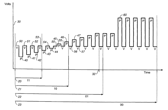
With reference to Fig. 1, in a multi-level
memory cell having two bits there are four memory states:
the "11" memory state 20, the "10" memory state 21, the
"01" memory state 22, and the "00" memory state 23. As
discussed above, in the 11 state, there is no charge on
the floating gate of the cell. The charge on the float-
ing gate increases through the states 10 and 01 until, at
state 00, the cell is fully charged. (Again, as noted
above, the terms "no charge" and "fully charged" are used
herein for the purposes of explanation and are not in-
tended to be limiting.) The present invention is based
on the realisation that after a memory cell has been
programmed to the next-to-last voltage memory state (in
Fig. 1, this would be the "01 state" 25), it is not nec-
essary to be as accurate in programming the cell to the
fully charged state.
In Fig. 1 it can be seen that in programming
the memory cell from the 11 state to the 10 state, a
method similar to the prior art is used in which a series
of programming pulses 40, 41, 42, increasing
incrementally in voltage, are applied to the control gate
of the memory cell in order to place a corresponding
amount of charge on the floating gate. In between each
of the programming pulses, a verify pulse 50, 51, 52 is
applied in order to check the state of the cell. This
program/verify process continues when the state of the
memory cell is going from 10 to 01. Once the cell has
reached the 01, or next-to-last, memory state (shown in
CA 02491228 2004-12-29
WO 2004/006266 PCT/US2003/013652
_7_
Fig. 1 to be at time 32), a programming pulse 60 having a
voltage level exceeding the threshold needed to place the
memory cell in the last memory state (00) is applied to
the memory cell. This allows the cell to reach the last
memory state (00) in a much more rapid fashion than in
the prior art. Because the slower program/verify ap-
proach is not necessary when programming the final maxi-
mum voltage memory state of the cell, by camping the
programming voltage up to the maximum threshold level
immediately following the cell reaching the next to last
state, the overall speed of programming the device memory
cell is increased.
With reference to Fig. 2, the voltage 34 of the
programming pulses is plotted with respect to time 37.
When programming the memory cell from the 11 state to the
10 state, and when programming from the 10 state to the
01 state, the graph of programming voltage versus time
would have a slope 80 that has a gradual increase, as is
expected when using the staircase program/verify method.
Then, when programming to the last state 00, the program-
ming voltage is camped up to the threshold voltage needed
to program the cell to the 00 state. The slope of the
line 85 is almost vertical and, as can be seen in the
graph, the cell is programmed to the voltage level 90 of
the 00 state very quickly.
It should be noted that slope of the line 80,
representing the programming of the intermediate states
10 and 01, can be steeper or flatter, depending on how
fast it is desired to program these intermediate levels.
Programming the intermediate levels using the prior art
staircase method requires a tradeoff between speed and
accuracy. Therefore, the line 80 would have a steeper
slope if more speed was desired, and would have less
slope if more accuracy, requiring program/verify pulses,
was desired.
As explained above, the memory cells in the 11,
10 and 01 states are programmed using the staircase pro-
gram/verify method. When it'is determined that all of
CA 02491228 2004-12-29
WO 2004/006266 PCT/US2003/013652
_g_
the 11, 10, and 01 memory cells have been programmed,
then this means that the only memory cells left to pro-
gram would be the 00 memory cells. This triggers the
change in the programming algorithm to ramp the program-
s ming voltage up to the threshold voltage needed to pro-
gram the cell to the 00 state. As shown in Fig. 2, the
ramping up to the maximum programming voltage may occur
at any point 'in the staircase programming algorithm 80,
depending on the programming speed of related memory
cells and data content. For example, line 81 shows the
voltage ramping step occurring soon after the beginning
of the programming cycle, indicating that all of the
cells need to be programmed to the 00 state. Line 82
illustrates a case having a programming speed not quite
as fast, while the example with line 85 is a slower pro-
gramming speed. The different lines shown in Fig. 2 are
due to variability in programming speed and in the data
to be programmed. Thus, the programming method of the
present invention compensates for variability in program-
ming speed in the memory array as the programming of the
last memory state occurs immediately after all of the
non-00 states have reached the desired programming lev-
els.
Referring to Fig. 2, if the programming of the
00 state had been done by continuing to use the prior art
staircase method, then the resulting slope 87 of the line
would be less steep, and the 00 state would not be pro-
grammed until a later point in time. Additionally, it is
possible that, using the staircase method, that the cell
could become saturated before reaching the 00 state, so
that the memory cell never reaches the last memory state.
By immediately ramping up the programming voltage to the
threshold voltage necessary to program the memory cell to
the 00 state, this eliminates the problem of memory cells
not reaching the programming level of the 00 state.
With reference to Fig. 3, a pair of signal
lines 210 and 220 are used for determining the program-
ming status of the memory cells connected to a particular
CA 02491228 2004-12-29
WO 2004/006266 PCT/US2003/013652
-9-
column of the memory array. The individual memory cells
are arranged in groups to be programmed. In the pre-
ferred embodiment, there are 32 memory cells in a group
such that each group constitutes eight bytes of informa-
tion. However, the groups can be of any size desired.
Fig. 3 shows a representation of the I/0 con-
trol circuits 201, 202-250 for each of the memory cells
291, 292-350 in a group. One or more gating transistors
375 are usually provided between each I/0 control cir-
suits 201 and its respective memory cell 291. The I/O
control circuits 201-250 each include sensing circuits
and state machines for decision making in order to con-
trol the programming of the respective memory cells. The
I/0 control circuits can be designed in a number of vari-
ous ways. The specific details of the I/0 control cir-
cuits relating to the invention will be described below.
Each I/0 control circuit 201-250 in a group of
memory cells is connected through a first transistor 222
to a multi-level ready signal line 220 and through a
second transistor 212 to an overall group ready signal
line 210. Each of the transistors 222 and 212 are n-
type MOS devices having a gate terminal connected to the
I/0 control circuit 201, a source terminal connected to
signal ground and a drain terminal connected to the re-
spective ready signal line 210, 220. The transistors 222
and 212 function as pull-down transistors, serving to
pull down the voltage of the ready signal lines 220, 210.
The multi-level ready signal line 220 indicates whether
the memory cell is ready for the programming transition
from the staircase programming method to the application
of a maximum voltage programming pulse. The overall
ready group signal line 210 indicates whether or not the
programming of all of the cells in a particular group has
been completed. Each signal line 210, 220 is connected
to a weak p-type MOS transistor 215, 225 which serves as
a pull-up transistor to pull up the voltage of the signal
lines. Each pull-up transistor 215, 225 has a drain
terminal connected to the respective signal line 210,
CA 02491228 2004-12-29
WO 2004/006266 PCT/US2003/013652
-10-
220, a gate terminal connected to signal ground, and a
source terminal connected to a power supply voltage 217,
227.
Each I/O control circuit 201-250 has a state
machine which communicates to a main memory controller
(not shown) through the mufti-level ready and overall
group signal lines 220 and 210. V~hen a memory cell has
finished programming, its I/0 control circuit 201 turns
off its respective n-type pull-down transistor 222 to
release that memory cell from the overall group signal
line 210. The overall group signal line 210 remains in a
low or "false" state if any of the pull down transistors
212 are on, since the pull down transistor 212 is a
stronger device than the pull-up transistor 215. When
all of the memory cells in a group on a column have been
programmed to the desired levels, then all of the pull-
down transistors 212 are off, and the overall group sig-
nal line 210 switches to a high, or "true", state. This
signals the main memory controller to trigger a reset to
allow the main memory controller to program the next
group of memory cells. The overall group signal line 210
remains low, or "false", when any of the memory cells
have not been fully programmed to the desired voltage
level.
The mufti-level signal line 220 is in a low
state when the pull-down transistor 222 for any of the
memory cells is on. A pull-down transistor 222 for a
particular I/O control device 207 turns off when it re-
ceives a low control signal from the I/O control device
201. This releases the I/0 device 201 from the multi-
level signal line 220. The pull-down transistor 222
receives the signal to turn off in one of two conditions.
In the first condition, when the memory cell is to be
programmed to the maximum voltage programming state (00),
then the I/O control device 201 immediately sends the
signal to release that I/0 control device from the multi-
level signal line 220. This is to signal that no further
CA 02491228 2004-12-29
WO 2004/006266 PCT/US2003/013652
-11-
multi-level programming is necessary. In the second
condition, when the memory cell is to be programmed to a
different state (11, 10, 01) than the maximum voltage
programming state, then the I/O control device turns off
the pull-down transistor 222 when the programming of that
particular memory cell has been completed. Similar to
the overall group signal line 210 described above, the
multi-level signal line 220 is in a low state until all
of the pull down transistors are off, and all of the I/0
control circuits/ memory cells have been released from
the signal line 220. Then, the voltage on the signal
line 220 is pulled up by pull-up transistor 225 to put
the multi-level signal line 220 is in a high state.
When the overall signal line 210 is low and the
mufti-level signal line 220 is low, then the group of
memory cells are programming using the program/verify
staircase method. V~hen the mufti-level signal 220 goes
to a high condition, this means that some of the cells
have been programmed to the desired states (11, 10 or 01)
and that the only cells left to be programmed are the 00
cells. At this point, the 00 cells have only been pro-
grammed to a non-determined state. Then the 00 cells
receive the increased programming voltage to put these
cells in the 00 state.
As an example of how the programming method of
the present invention works, with reference to Fig. 3,
assume that the memory cells for I/0 control circuits 201
and 250 are to be programmed to~the maximum voltage mem-
ory state (00), the memory cell for I/0 control circuit
202 is to be programmed to the 01 state, and the rest of
the group (not shown) are to be programmed to the 10
state. The overall group signal line 210 is reset and is
in a low condition, meaning that the programming of the
group is not complete. The I/0 control circuits 201 and
208 immediately send signals to the mufti-level signal
line 220 to release those memory cells from mufti-level
signal line 220, since those memory cells will be pro-
grammed to the maximum state (00). The programming of
CA 02491228 2004-12-29
WO 2004/006266 PCT/US2003/013652
-12-
the group of memory cells begins using the program/verify
staircase method. When the programming voltage reaches
the level in which those memory cells to be programmed to
the 10 state have been programmed, then the I/O control
circuits of those memory cells send signals to release
their respective transistors from the multi-level signal
line 220. However, due to variability in programming
speed, this may not necessarily occur at the same moment
in time. Thus, in this case, it is likely that the pull-
down transistor 223 for I/0 control circuit 202 is the
only pull-down transistor still on. The program/verify
staircase method continues until the memory cell for I/O
control circuit 202 is programmed to the desired state
(01). At this point, transistor 223 turns off and the
multi-level signal line goes high. This signals a change
in the programming method to instruct the memory control-
ler to provide the maximum voltage programming pulse for
programming the 00 memory cells 201, 250. When the mem-
ory cells 201, 250 have been programmed, then all of
memory cells 201-250 in the group have been programmed
and the respective Il0 control circuit turns off the
pull-down transistor 212 connected to the overall group
signal line 210. Then, the overall group signal line 210
pulls up to a high condition, which signals the main
memory controller that the programming has been completed
and triggers a reset of the signal lines 210, 220.
In a preferred embodiment of the present inven-
tion, the bitline voltages supplied to each of the memory
cells would be different for each different memory state.
The lower memory states 11 and 10 would have lower
bitline voltages in order to slow down the programming
algorithm and provide better control, while higher
bitline voltages would be used for the higher memory
states 01 and 00. However, the present invention may
also be implemented using the same bitline voltage for
each different state, or using other variations of the
bitline voltage from that described above.
CA 02491228 2004-12-29
WO 2004/006266 PCT/US2003/013652
-13-
The programming method of the present invention
allows the overall programming of the cell to be faster
than that of the prior art programming methods. However,
it also allows for the accuracy needed in programming the
intermediate states of 01 and 10. Thus, the present
invention provides both accuracy and increased speed, and
provides an improvement over the prior art method of
programming mufti-level memory cells. The memory cell
described above having two bits and four memory states is
exemplary, and the programming method of the present
invention can be implemented with mufti-level memory
cells having any number of bits and corresponding memory
states.