Note: Descriptions are shown in the official language in which they were submitted.
CA 02491923 2005-O1-05
WO 2004/040413 PCT/US2003/033941
COMPUTER SYSTEM ARCHITECTURE AND MEMORY CONTROLLER
FOR CLOSE-COUPLING WITHIN A HYBRID PROCESSING SYSTEM
UTILIZING AN ADAPTIVE PROCESSOR INTERFACE PORT
CROSS REFERENCE TO RELATED PATENT APPLICATIONS
The present invention claims priority from, and is a continuation-in-part
application of, U.S. Patent Application Ser. No. 09/755,744 filed January 5,
2001 for: "Multiprocessor Computer Architecture Incorporating a Plurality of
Memory Algorithm Processors in the Memory Subsystem" which is a
divisional application of U.S. Patent Application Ser. No. 09/481,902 filed
to January 12, 2000 (now U.S. Patent No. 6,247,110) which is a continuation
application of U.S. Patent Application Ser. No. 08/992,763 filed December 17,
1997 (now U.S. Patent No. 6,076,152). The present invention is related to
the subject matter of U.S. Patent No. 6,339,819 issued January 15, 1992 for:
"Multiprocessor with Each Processor Element Accessing Operands in Loaded
is Input Buffer and Forwarding Results to FIFO Output Buffer". The foregoing
patent application and issued patents are assigned to SRC Computers, Inc.,
assignee of the present invention, the disclosures of which are herein
specifically incorporated in their entirety by this reference.
BACKGROUND OF THE INVENTION
2 o The present invention relates, in general, to the field of computer
systems and techniques for interconnecting various processing or computing.
elements. More particularly, the present invention relates to a hybrid
computer system architecture and memory controller for close-coupling within
a hybrid computing system using an adaptive processor interface port.
2 s Hybrid computer systems are those that incorporate both standard
microprocessors and adaptive processors. These are typically large
multiprocessor server-type systems that reside on a shared network and are
not directly operated with a user interface console. The overall performance
and flexibility of such systems is directly proportional to the level of
coupling
3 o between the microprocessors and the adaptive processors. That is to say,
if
1
CA 02491923 2005-O1-05
WO 2004/040413 PCT/US2003/033941
the two processor types are treated as peers and have equal bandwidths and
latencies to a shared memory, the system performance will be maximized.
To date, there have been several accepted methodologies for coupling
the two forms of processors. The most basic of which was to connect the
s adaptive processor via the standard input/output ("I/O") ports to the
microprocessor. This is relatively simple in practice but provides only a very
loose coupling with low bandwidths and high latencies relative to the
bandwidths and latencies of the processor bus. Since both types of
processors must share the same memory, this leads to significantly reduced
1 o performance in the adaptive processors. This technique also limits the
amount of processor interaction that can realistically occur.
The second typical method of interconnection is to place the adaptive
processor in the memory space of the microprocessor such as disclosed in
certain specific embodiments disclosed in the aforementioned patents and
15 patent applications. This connection yields a much tighter coupling as well
as
bandwidths and latencies typically equal to the microprocessor bus. However,
particularly for small transfers, there may be more overhead associated with
this connection than is desired. This is due to the "slaved" nature of the
standard memory subsystem in a personal computer environment.
2 o The third known method is to place the adaptive processor directly on
the microprocessor bus or primary microprocessor interconnect (e.g. the
Front Side Bus "FSB"). This method would seem to insure that the adaptive
processor will have the same bandwidth and latency to the rest of the system
as the microprocessors. However, in reality, this may not be true. In the case
2s of Intel~ microprocessors, a foreign device such as the adaptive processor,
may be subject to special treatment and is classified as a third party agent.
As such, it may not be able to use many features of the bus such as those
associated with movement of cached data or data movement to I/O devices. It
may also be the case that the adaptive processor is itself a whole circuit
3 o board and connection of it to the microprocessor may violate the bus
layout
ground rules. In addition, the adaptive processor would also have to
participate in all of the microprocessor bus protocol, such as correctly
2
CA 02491923 2005-O1-05
WO 2004/040413 PCT/US2003/033941
responding to cache coherency related transactions, even though it may not
be a coherent bus agent.
SUMMARY OF THE INVENTION
There is however a way to accomplish the desired coupling while
eliminating issues associated with residing on the microprocessor bus. This is
through the use of a dedicated adaptive processor interface port ("APIP")
added to, or in conjunction with, the memory and I/O controller chip of the
core logic, typically called the "North Bridge", on Intel~ based processor
boards today. Memory accesses to and from this port as well as the main
to microprocessor bus, are then arbitrated by the circuitry inside the memory
controller. In this fashion, both the microprocessors and the adaptive
processors exhibit equal memory bandwidth and latency. In addition,
because it is a separate electrical port from the microprocessor bus, the APIP
is not required to comply with, and participate in, all FSB protocol. This
results in reduced protocol overhead which results higher yielded payload on
the interface.
To accelerate data movement to the adaptive processor, it is also
possible to include a Direct Memory Access ("DMA") engine inside the North
Bridge. This would allow the adaptive processor to issue a single "read"
2 o request over the API P that would result in the DMA engine actually
retrieving
and transmitting a large data block to the adaptive processor. This DMA
engine can handle both a "read" and "write" request simultaneously to allow
streaming operations to occur as efficiently as possible within the adaptive
processor.
2 s To allow very large systems to be constructed, this port can be
provided with enough drive capability to allow it to be connected to an
external interconnect such as a large crossbar switch. In this fashion, many
of the adaptive processors and microprocessors can work in a randomly
interconnected way to solve problems. Due to the potential for any given port
3 0 of the switch to be busy at any point in time, it may be desirable for the
outbound path of the APIP to be equipped with a small buffer to allow the
CA 02491923 2005-O1-05
WO 2004/040413 PCT/US2003/033941
completion of "read" memory accesses that may be underway when the path
goes busy without the loss of data. As soon as the path is free, the buffer
can
be drained and transmitted and the current DMA resumed. One way to
indicate a busy path could be communicated through the use of a "busy"
signal sent from the busy receiver port to the transmitter to which it is
connected. Consequently, the APIP will stop transmission when it receives a
"busy" signal and will generate a separate "busy" signal when it can no longer
receive data for whatever reason.
To aid in control of the adaptive processor as well as in direct
to communication between the adaptive processor and the microprocessor, a
series of preferably 64 bit registers should be included in the memory
controller. These registers could then be made accessible from either the
microprocessor or the adaptive processor.
Typically there is a need for processors to interrupt each other in a
1 s large system. The same is true when dealing with a hybrid system.
Therefore, the APIP can be provided with the ability to accept inter-processor
interrupts from the microprocessor and send them to other processors in the
system as well as performing the reverse function and receive inter-processor
interrupts. This port could be similar in physical appearance to an AGP
2 o graphics port. In fact, since the accelerated graphics port ("AGP") is
typically
not used on servers due to the absence of monitors, it would actually be
possible to use the same device pins on the memory controller and use a
register to allow the port to be configured as either AGP or APIP.
Particularly disclosed herein is a computer system which comprises at
2s least one microprocessor presenting a first bus, a memory controller
coupled
to the first bus and also coupled to a memory bus and an adaptive processor
port, a memory block coupled to the memory bus and an adaptive processor
coupled to the adaptive processor port.
Further disclosed herein is a hybrid computing system comprising at
3 0 least one microprocessor, a memory block, a memory controller coupled to
the
microprocessor and the memory block for controlling accesses to the memory
CA 02491923 2005-O1-05
WO 2004/040413 PCT/US2003/033941
block by the at least one microprocessor and at least one adaptive processor
coupled to the memory controller with the memory controller further
controlling
accesses to the memory block by the at least one adaptive processor.
Still further disclosed herein is a computing system comprising first and
second processing elements, a memory block and a memory controller
coupled to the first processing element through a first bus and the second
processing element through a second bus with the memory controller
controlling accesses to the memory block by the first and second processing
elements.
1 o Also disclosed herein is a memory controller for a computing system
comprising a memory bus arbitrator coupled between first and second
processing elements and a memory block with the memory bus arbitrator
controlling access to the memory block by the first and second processing
elements.
BRIEF DESCRIPTION OF THE DRAWINGS
The aforementioned and other features and objects of the present
invention and the manner of attaining them will become more apparent and
the invention itself will be best understood by reference to the following
description of a preferred embodiment taken in conjunction with the
2 o accompanying drawings, wherein:
Fig. 1 is a high-level functional block diagram of a typical computing
system, for example, a personal computer ("PC") implemented in conjunction
with a memory and input/output ("I/O") controller ("North Bridge") and a
peripheral component interconnect ("PCI") bus I/O controller ("South Bridge");
Fig. 2 is a functional block diagram of a typical I/O connected hybrid
computing system comprising a number of microprocessors and adaptive
processors, with the latter being coupled to an I/O bridge;
Fig. 3 is a functional block diagram of a typical memory connected
hybrid computing system comprising a number of microprocessors and
3 o adaptive processors, with the latter being coupled to the system memory;
5
CA 02491923 2005-O1-05
WO 2004/040413 PCT/US2003/033941
Fig. 4 is a functional block diagram of a typical Front Side Bus ("FSB")
connected hybrid computing system comprising a number of microprocessors
and adaptive processors, with the latter being coupled directly to the FSB;
Fig. 5 is a corresponding functional block diagram of an adaptive
processor interface port ("APIP") connected hybrid computing system in
accordance with the present invention comprising a number of
microprocessors and adaptive processors, with the latter being coupled
directly to a memory and I/O controller;
Fig. 6 is a functional block diagram of a memory and I/O controller
to implementing an APIP interface for use with an adaptive processor;
Fig. 7 is a functional block diagram of a multi-adaptive processor
(MAPT"", a trademark of SRC Computers, Inc.) for possible use as an
adaptive processor in a hybrid computing system in accordance with the
present invention; and
Fig. 8 is a functional block diagram of a portion of an adaptive processor
interface port connected hybrid computing system in accordance with another
embodiment of the present invention wherein the functions of the memory and
I/O controller have been incorporated into the microprocessor itself.
DESCRIPTION OF A REPRESENTATIVE EMBODIMENT
2o With reference now to Fig. 1, a high-level functional block diagram of a
typical computing system 100 is shown. The computing system 100 may be,
for example, a personal computer ("PC") which incorporates a commercially
available integrated circuit ("IC") memory controller ("North Bridge") 102
such
as the P4X333JP4X400 devices available from VIA Technologies, Inc.; the
M1647 device available from Acer Labs, Inc. and the 824430X device
available from Intel Corporation. The North Bridge IC 102 is coupled by
means of a Front Side Bus ("FSB") to a processor 104 such as one of the
Pentium~ series of processors also available from Intel Corporation.
The North Bridge IC 102 is coupled via a separate memory bus to
3 o system memory 106 which may comprise, for example, a number of
6
CA 02491923 2005-O1-05
WO 2004/040413 PCT/US2003/033941
synchronous dynamic random access ("SDRAM") memory modules. A
dedicated accelerated graphics port ("AGP") is provided for interfacing the
system 100 to a graphics accelerator while an inter-bridge bus couples the
North Bridge IC 102 to an additional input/output I/O controller IC ("South
Bridge") 108. The South Bridge IC may be, for example, an SLC90E66
device available form Standard Microsystems, Corporation or the VT8235
device available from VIA Technologies.
The South Bridge IC 108 couples the system 100 to a peripheral
component interconnect ("PCI") bus for interfacing to a number of dedicated
Zo PCI slots 110. Interconnections with a universal serial bus ("USB"), system
management ("SM") bus and general purpose ("GP") I/O bus are also provided
as well as to an industry standard architecture/extended Il0 ("ISA/E10") bus
to
a basic input/output system ("BIOS") block 112 and a system controller 114
which controls a number of the various components of the system 100.
15 With reference additionally now to Fig. 2, a functional block diagram of
a typical I/O connected hybrid computing system 200 is shown. The hybrid
computing system 200 comprises one or more North Bridge ICs 2020 through
202N, each of which is coupled to four microprocessors 20400 through 20403
through and including 204NO through 2043 by means of a Front Side Bus.
2 o The North Bridge ICs 2020 through 202N are coupled to respective blocks of
memory 2060 through 206N as well as to a corresponding I/O bridge element
2080 through 208N. A network interfiace card ("N1C") 2120 through 212N
couples the I/O bus of the respective I/O bridge 2080 through 208N to a
cluster bus coupled to a common clustering hub (or Ethernet Switch) 214.
25 As shown, an adaptive processor element 2100 through 210N is
coupled to, and associated with, each of the I/O bridges 2080 through 208N.
This is the most basic of the existing approaches for connecting an adaptive
processor 210 in a hybrid computing system 200 and is implemented,
essentially via the standard I/O ports to the microprocessors) 204. While
3 o relatively simple to implement, it results in a very "loose" coupling
between the
adaptive processor 210 and the microprocessors) 204 with resultant low
bandwidths and high latencies relative to the bandwidths and latencies of the
CA 02491923 2005-O1-05
WO 2004/040413 PCT/US2003/033941
processor bus. Moreover, since both types of processors 204, 210 must
share the same memory 206, this leads to significantly reduced performance
in the adaptive processors 210. Functionally, this architecture effectively
limits the amount of interaction between the microprocessors) 204 and the
adaptive processor 210 that can realistically occur.
With reference additionally naw to Fig. 3, a functional block diagram of
a typical memory connected hybrid computing system 300 is shown. The
hybrid computing system 300 also comprises a number of North Bridge ICs
2020 through 202N, each of which is coupled to four microprocessors 20400
to through 20403 through and including 204N0 through 204N3 by means of a Front
Side Bus. The North Bridge ICs 2020 through 202N are coupled to respective
blocks of memory 2060 through 206N as well as to a corresponding I/O bridge
element 2080 through 208N. A network interface card ("NIC") 2120 through
212N couples the I/O bus of the respective I/O bridge 2080 through 208N to a
cluster bus coupled to a common clustering hub (or Ethernet Switch) 214.
As shown, an adaptive processor element 3100 through 310N is
coupled to, and associated with, each of the blocks of memory 2060 through
206N. In this particular computing system 300 architecture, the adaptive
processor 310 is effectively placed in the memory 206 space of the
2 o microprocessors) 204 in a manner as disclosed in certain of the afore-
mentioned patents. The architecture of the computing system 200 shown
yields a much tighter coupling between the microprocessors) 204 and the
adaptive processor 310 than that of the computing system 200 of the
preceding figure as well as providing bandwidths and latencies typically equal
2 5 to the microprocessor bus itself. Nevertheless, particularly for small
transfers,
there may be more overhead associated with this type of interconnection than
is desired due to the effectively "slaved" nature of the standard memory
subsystem in a personal computing environment.
With reference additionally now to Fig. 4, a functional block diagram of
3 o a typical Front Side Bus ("FSB") connected hybrid computing system 400 is
shown. The hybrid computing system 400 again comprises a number of
North Bridge ICs 2020 through 202N, each of which is coupled to four
s
CA 02491923 2005-O1-05
WO 2004/040413 PCT/US2003/033941
microprocessors 20400 through 20403 through and including 204N0 through
204N3 by means of a Front Side Bus. The North Bridge ICs 2020 through
202N are coupled to respective blocks of memory 2060 through 206N as well
as to a corresponding I/O bridge element 2080 through 208N. A network
interface card ("NIC") 2120 through 212N couples the I/O bus of the respective
I/O bridge 2080 through 208N to a cluster bus coupled to a common clustering
hub (or Ethernet Switch) 214.
As shown, an adaptive processor element 2100 through 210N is coupled
to, and associated with, each of the Front Side Buses coupled to the
z o microprocessors 20400 through 20403 through and including 204N0 through
204N3. In this particular architecture, the adaptive processor 410 is placed
directly on the microprocessor 204 bus or Front Side Bus. This
interconnection scheme would seem to insure that the adaptive processor 410
will have the same bandwidth and latency to the rest of the computing system
400 as the microprocessors) 204. However, in reality this may not be true. In
the case of Intel~ microprocessors, a "foreign" device such as the adaptive
processor 410, may be subject to special treatment and is classified as a
"third
party agent". As such, it may not be able to use many features of the Front
Side Bus such as those associated with the movement of cached data or data
2 o movement to I/O devices. It may also be the case that the adaptive
processor
410 is itself an entire circuit board and connection of it to the
microprocessor
may violate the bus layout ground rules. In addition, the adaptive processor
410 would also have to participate in all of the microprocessor 204bus
protocol, such as correctly responding to cache coherency related
2 s transactions, even though it may not itself be a coherent bus agent.
With reference additionally now to Fig. 5, a corresponding functional
block diagram of an adaptive processor interface port ("APIP") connected
hybrid computing system 500 in accordance with the present invention. The
computing system 500 comprises a number of memory and I/O controllers
3 0 5020 through 502N, each of which is coupled to four microprocessors 20400
through 20403 through and including 204N0 through 204N3 by means of a Front
Side Bus. The memory and I/O controllers 5020 through 502N are coupled to
9
CA 02491923 2005-O1-05
WO 2004/040413 PCT/US2003/033941
respective blocks of memory 2060 through 206N as well as to a corresponding
I/O bridge element 2080 through 208N. A network interface card ("NIC") 2120
through 212N couples the I/O bus of the respective I/O bridge 2080 through
208N to a cluster bus coupled to a common clustering hub (or Ethernet
Switch) 214.
As shown, an adaptive processor element 5100 through 510N is
coupled to, and associated with, each of the memory and I/O controllers 5020
through 502N through an adaptive processor interface port ("APIP") thereby
improving the computing system 500 performance and eliminating the
to disadvantages of the foregoing conventional techniques. In other
implementations of the present invention, one or more of the adaptive
processors) 510 may be replaced with a conventional microprocessor
coupled to the APIP interface.
In a preferred embodiment as disclosed herein, this may be
effectuated through the use of a dedicated adaptive processor interface port
added to, or associated with, the memory and I/O controller 502 (such as a
North Bridge chip). Memory accesses to and from this APIP port, as well as
those to and from the main microprocessor 204 bus (e.g. the Front Side Bus),
are then arbitrated by the memory control circuitry inside the memory and I/O
2o controller 502. In this fashion, both the microprocessors) 204 and the
adaptive processors) 510 would have equal memory bandwidth and latency.
In addition, because it is a separate electrical port from that of the
microprocessor bus, the APIP is not required to comply with, and participate
in, all FSB protocols. This results in reduced protocol overhead which, in
turn,
2 s results in a higher yielded payload on the interface.
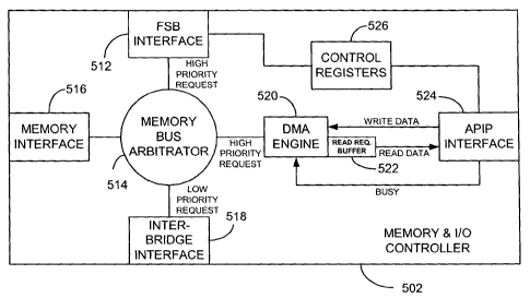
With reference additionally now to Fig. 6, a functional block diagram of
the memory and I/O controller 502 implementing an APIP interface of the
preceding figure is shown. The memory and I/O controller 502 includes an
FSB interface 512 controlled by a memory bus arbitrator 514 for responding
3 o to high priority requests to/from the microprocessors 20400 through 20403
through and including 204NO through 204N3. The memory bus arbitrator 514
also controls a memory interface 516 for providing access to the blocks of
CA 02491923 2005-O1-05
WO 2004/040413 PCT/US2003/033941
memory 2060 through 206N. Low priority requests through the I/O bridge
elements 2080 through 208N are made through an inter-bridge interface 518
as controlled by the memory bus arbitrator 514.
In lieu of, or in addition to, the conventional AGP bus interface, the
memory and UO controller 502 includes an APIP interface 524 as shown for
interfacing and communication with an adaptive processor element 5100
through 510N. A direct memory access ("DMA") engine 520, in conjunction
with a read request buffer 522 for "reads" handles high priority requests to
and from the memory bus arbitrator 514 and the APIP interface 524 over, for
to example, separate "write data" and "read data" buses. The APIP intertace
524 may, in an exemplary embodiment, include the provision of a "busy"
signal from the APIP interface to the DMA engine 520. Further, a number of
control registers 526 may also be provided coupling the FSB interface 512 to
the APIP interface 524.
In operation, the DMA engine 520 can serve to accelerate data
movement to the adaptive processor 510 through the memory and I/O
controller 502. This functionality allows the adaptive processors) 510 to
issue a single "read" request over the APIP interlace 524 that would result in
the DMA engine 520 actually retrieving and transmitting a large data block to
2 o the adaptive processor 510. The DMA engine 520 can handle both a "read"
and "write" request simultaneously in order to allow streaming operations to
occur as efficiently as possible within the adaptive processor 510.
To allow very large computing systems 500 to constructed, the APIP
interface 524 can be provided with sufficient drive capability to allow it to
be
2s connected to an external interconnect, for example, a large crossbar
switch.
In this fashion, many of the adaptive processors) 510 and microprocessors)
204 can work in a randomly interconnected way to solve problems. Due to
the potential for any given port of the switch to be busy at any point in
time, it
may be desirable for the outbound path of the APIP interface 524 to be
3 o equipped with a small buffer (e.g, read request buffer 522) to allow the
completion of "read" memory accesses that may be underway when the path
goes "busy" without the loss of data. As soon as the path is free, the buffer
m
CA 02491923 2005-O1-05
WO 2004/040413 PCT/US2003/033941
522 can be drained and transmitted and the current DMA operation resumed.
One way to indicate a busy path could be communicated through the use of a
"busy" signal sent from the busy receiver port to the transmitter to which it
is
connected. Consequently, the APIP interface 524 will stop transmission
when it receives a "busy" signal and will generate a separate "busy" signal
when it can no longer receive data for whatever reason.
To aid in control of the adaptive processor 510 as well as in direct
communication between the adaptive processors) 510 and the
microprocessors) 204, a series of, for example, 64 bit control registers 526
1 o may be included as a portion of the memory and I/O controller 502. These
registers 526 would be ideally accessible from either the microprocessors)
204 or the adaptive processors) 510. Typically there is a need for
processors 204 to interrupt each other in a relatively large computing system
500. The same is true when dealing with a hybrid computing system.
is Therefore, the APIP interface 524 can be provided with the ability to
accept
inter-processor 204 interrupts from the microprocessor 204 and send them to
other processors 204 in the system as well as performing the reverse function
and receive inter-processor 204 interrupts.
In a particular implementation, the APIP interface 524 may be similar in
2o physical appearance to an AGP graphics port. In fact, since the accelerated
graphics port ("AGP") is typically not used on servers due to the absence of
monitors, it is possible to use the same pins otherwise available on a typical
North Bridge device and use a register in order to enable the port to be
configured as either AGP or APIP.
25 With reference additionally now to Fig. 7, a functional block diagram of
a multi-adaptive processor element (MAPTM, a trademark of SRC Computers,
Inc.) for possible use as an adaptive processor element 510 is shown. The
adaptive processor element 510 includes a user array 539 which may
comprise one or more field programmable gate arrays ("FPGAs") as disclosed
3 o in the foregoing issued patents and pending patent application. A chain
port
may be provided for directly coupling two or more adaptive processor
elements 510 as shown.
12
CA 02491923 2005-O1-05
WO 2004/040413 PCT/US2003/033941
A control chip 532 couples the adaptive processor element 510 to the
APIP interface 524 of the associated memory and I/O controller 502 and
provides control functionality to the corresponding user array 530. On-board
memory 534 is coupled to the control chip 532 and user array 530, for
s example, though six ports. Briefly, the write data and read data lines of
the
memory and I/O controller 502 are coupled to the control chip (or block) 532
which provides addresses to the on-board memory 534 and receives
addresses from the user array 530 on a number of address lines. Data
supplied on the write data line is provided by the control chip 532 to the on-
1 o board memory 534 on a number of data lines and data read out of the on-
board memory 534 is provided on these same lines both to the user array 530
as well as the control chip 532 for subsequent presentation to the APIP
interface 524. As indicated, a chain port may be coupled to the user array
530 for communication of read and write data directly with one or more other
1 s adaptive processors 510.
With reference additionally now to Fig. 8, a functional block diagram of
a portion of an adaptive processor interface port connected hybrid computing
system 800 in accordance with another embodiment of the present invention
is shown. In the computing system 800, the functions of the memory and I/O
2 o controller 802 have been incorporated into the microprocessor 804 as
shown.
In this manner, a memory interface 516 of the memory and l/O controller 802
may be coupled to a memory block 806, an inter-bridge interface 518 may be
coupled to an I/O bridge 808 and an APIP interface 524 may be coupled to an
adaptive processor 810. fn the computing system 800, the functionality of the
25 memory and I/O controller 502 (Fig. 6) is maintained but, by integrating
its
functionality into the microprocessor 804 by the inclusion of an integral
memory and I/O controller 802, the need for a separate chip or integrated
circuit device is eliminated.
While there have been described above the principles of the present
3 o invention in conjunction with specific computing system architectures and
components, it is to be clearly understood that the foregoing description is
made only by way of example and not as a limitation to the scope of the
13
CA 02491923 2005-O1-05
WO 2004/040413 PCT/US2003/033941
invention. Particularly, it is recognized that the teachings of the foregoing
disclosure will suggest other modifications to those persons skilled in the
relevant art. Such modifications may involve other features which are already
known per se and which may be used instead of or in addition to features
s already described herein. Although claims have been formulated in this
application to particular combinations of features, it should be understood
that
the scope of the disclosure herein also includes any novel feature or any
novel combination of features disclosed either explicitly or implicitly or any
generalization or modification thereof which would be apparent to persons
to skilled in the relevant art, whether or not such relates to the same
invention
as presently claimed in any claim and whether or not it mitigates any or all
of
the same technical problems as confronted by the present invention. The
applicants hereby reserve the right to formulate new claims to such features
and/or combinations of such features during the prosecution of the present
15 application or of any further application derived therefrom.
What is claimed is:
14