Note: Descriptions are shown in the official language in which they were submitted.
CA 02492042 2005-01-06
WO 2004/006452 PCT/US2003/021864
TITLE OF THE INVENTION
A Control System for Controlling an Output Signal Power Level of a Wireless
Transmitter
FIELD OF THE INVENTION
[0001] The present invention relates to the field of wireless transmitters.
More
specifically, the present invention relates to the field of two-way satellite
communication
systems and other transmission systems where the maxiinum transmit signal
power level is
regulated.
BACKGROUND OF THE INVENTION
[0002] Two-way satellite communication systems transmit and receive data in
various frequency bands. For example, some systems operate in the Ka band,
which is
between about 17 and 36 GHz. Other systems operate in bands such as the C-band
(3.7 - 6.4
GHz) or the Kõ-band (11 - 15 GHz), for example. Future systems may use higher
frequencies
(e.g., 60 GHz).
[0003] Modulation and upconversion are essential methods used in two-way
satellite communication systems and in other wireless communication systems.
Upconversion is the translation of a signal's frequency from baseband, or the
original
frequency before modulation, to a higher frequency. The signal is then
transmitted at this
higher frequency. Upconversion is performed because most antennas can only
receive signals
that have short wavelengths. Frequency is the inverse of wavelength.
Therefore, the higher
the frequency a signal has, the shorter its wavelength. Consequently, signals
upconverted to a
higher frequency are easier to transmit.
[0004] Modulation is a method used to transmit and receive data using a
carrier
signal. Modulated signals can be analog or digital signals. By varying the
phase of a digital
carrier signal, for example, information can be conveyed. This type of
modulation is called
phase-shift keying (PSK). There are several schemes that can be used to
accomplish PSK.
The simplest method uses only two signal phases: 0 degrees and 180 degrees.
The digital
signal is broken up time wise into individual bits (binary digits-zeros and
ones). . The state
1
CA 02492042 2005-01-06
WO 2004/006452 PCT/US2003/021864
of each bit is determined according to the state of the preceding bit. If the
phase of the wave
does not change, then the signal state stays the same (low or high). If the
phase of the wave
changes by 180 degrees-that is, if the phase reverses then the signal state
changes (from
low to high, or from high to low). Because there are two possible wave phases,
this form of
PSK is sometimes called Binary Phase Shift Keying (BPSK).
[0005] A more complex form of PSK is called Quadrature Phase Shift Keying
(QPSK). QPSK modulation employs four wave phases and allows binary data to be
transmitted at a faster rate per phase change than is possible with BPSK
modulation. In
QPSK modulation, the signal to be transmitted is first separated into two
signals: the In-phase
(I) signal and the Quadrature (Q) signal. The I and Q signals are orthogonal,
or 90 degrees
out of phase. Thus, they are totally independent and do not interfere with
each other. Each
signal can then be phase shifted independently. Both the I and Q signals have
two possible
phase states. Combining the possible states for the I and Q signals results in
four total
possible states. Each state can then represent two bits. Thus, twice the
information can be
ZS conveyed using QPSK modulation instead of BPSK modulation. For this reason,
QPSK
modulation is used in many two-way satellite communication systems.
[0006] Currently, upconversion in most two-way satellite communication systems
entails a multi-stage conversion process. First, baseband QPSK I, Q streams
are modulated
and then upconverted to a.n Intermediate Frequency (IF) (e.g., 1.7-2.2 GHz).
This conversion
is performed by in an Indoor Unit (IDiJ). The signal is then upconverted again
to a transmit
frequency, fTx (e.g., 29.5-30.0 GHz), in an Outdoor Unit (ODU) located at the
terminal's
antenna. The upconversion is then complete and the signal is ready for
transmission.
[0007] The output signal (transmit signal) of the ODU has associated with it a
certain power level. The ODU output signal power level is regulated in many
countries and
cannot exceed certain levels. The maximum allowable output signal power level
varies by
country.
[0008] In many two-way satellite communication systems, for example, the
optimal output signal power level of the ODU is 4 watts. Some countries allow
this output
signal power level. However, other countries are more limiting in their
regulations and allow
ODU output signal power levels of no more than 2 watts, for example.
2
CA 02492042 2005-01-06
WO 2004/006452 PCT/US2003/021864
[0009] A high ODU output signal power level is preferable to a low ODU output
signal power level because the higher output signal power level is easier to
detect and receive.
A high ODU output signal power level requires a smaller receiving antenna than
does a small
ODU output signal power level. Small anteimas are usually easier and more cost-
effective to
s design and construct than are large antennas.
[0010] The same various limitations on transmitter output signal power levels
could be imposed on any transmitting device used in wireless communication
systems. Thus,
as used hereafter and in the appended claims, the term "two-way satellite
communication
systems" will be used to refer expansively to all possible two-way satellite
coinmunication
systems and other applications where the maximum output signal power level of
a transmitter
is regulated. In addition, the term "ODU" will be used to refer expansively to
all possible
transmitters.
[0011] Thus, there is a need in the art for a method and system of limiting
the
ODU output signal power level to various levels so that it is always equal to
the maximum
allowable power level depending on the country within which the two-way
satellite
communication system operates.
[0012] There have been several approaches to complying with the various ODU
output signal power level restrictions. One solution is to fix the ODU output
signal power
level to equal the lowest maximum allowable output signal power level of the
countries
within which the two-way satellite communication system might operate. For
example, if the
lowest maximum allowable output signal power level is 2 watts, the ODU
amplification
circuitry could be modified so that the maximuin power level of the output
signal never
exceeds 2 watts. This ODU output signal power level is obviously not optimal
in the
countries with higher maximum allowable output signal power levels.
[0013] Another traditional solution to limit the ODU output signal power level
to
various levels is to use Automatic Gain Control (AGC). AGC is a process or
means by which
the gain (output power versus input power) of the ODU is automatically
adjusted as a
function of a specified paraineter, such as the output signal leve,l. However,
AGC cannot be
used in the ODU of many two-way satellite communication systems because it
takes too long
to lock into the desired gain. Also, the ODU output signal power level needs
to change
3
CA 02492042 2005-01-06
WO 2004/006452 PCT/US2003/021864
according to varying weather conditions. It is currently difficult, if not
impossible, for an
AGC circuit to adjust for varying weather conditions.
[0014] Another possible solution is an IDU that is capable of adjusting the
ODU
input signal level power. This requires a means for calculating the ODU gain
and an interface
unit for communicating this gain information to the IDU. The IDU would then
need to adjust
the ODU input signal power level based on this gain information so that the
ODU output
signal power level can change to the desired level. However, this process is
currently limited
by the speed at which the interface unit between the IDU and ODU operates and
is therefore
too slow for many applications. In addition, it requires an IDU capable of
adjusting the input
signal level power of the ODU. This capability might not be present in many
systems.
[0015] Another possible solution that has been explored is to monitor the
direct
current (DC) current of the output signal of the ODU. Then, according to the
monitored DC
current, the IDU varies the output signal level which is input into the ODU to
adjust the
power level of the output signal.
[0016] For example, if the power level of the output signal is desired to be
less
than 2 watts, but it is currently higher than 2 watts, then the DC current of
the output signal is
higher than it would be at the desired power level. Reducing the ODU input
signal power
level decreases the ODU output signal power level as well as the DC current of
the output
signal.
[0017] However, in many two-way satellite communication systems, it is
difficult
to correlate the DC current and the radio frequency (RF) output signal power.
This is, in part,
due to the use of a class-A wideband power amplifier (PA) in the ODU. Class-A
PAs are
used because they reproduce the input signal with little distortion. They are,
however, the
least efficient among the different classes of PAs because the power of their
output signals is
only a small percentage of the DC power used in the amplification process. The
degree of
inefficiency varies from PA to PA and thus, the correlation between the DC
current of the
output signal and its power level is unpredictable.
4
CA 02492042 2005-05-31
SUMMARY OF THE INVENTION
[0001] A wireless transmitter system includes an outdoor unit configured to
process an input signal having an associated input signal power level and
generate an output
signal having an associated output signal power level. The output signal power
level initially
depends on the input signal power level. The system further includes an indoor
unit for
generating the input signal and initializing the input signal power level such
that the output
signal power level is substantially equal to a predetermined threshold. After
the indoor unit
initializes the input signal power level, the outdoor unit independently
controls the output
signal power level using an attenuator in accordance with a comparison of the
output signal
power level and the predetermined threshold.
[0002] Additional advantages and novel features of the invention will be set
forth
in the description which follows or may be learned by those skilled in the art
through reading
these materials or practicing the invention. The advantages of the invention
may be achieved
through the means recited in the attached claims.
BRIEF DESCRIPTION OF THE DRAWINGS
[0003] The accompanying drawings illustrate preferred embodiments of the
present invention and are a part of the specification. Together with the
following description,
the drawings demonstrate and explain the principles of the present invention.
The illustrated
embodiments are examples of the present invention and do not limit the scope
of the
invention.
[0004] Fig. 1 is a block diagram of a multi-stage modulator and upconverter
that
is used in an exemplary two-way satellite communication system and that could
be used to
implement an embodiment of the present invention.
[0005] Fig. 2 is a detailed block diagram of ODU components, all or some of
which might be used to implement an embodiment of the present invention.
5
CA 02492042 2005-01-06
WO 2004/006452 PCT/US2003/021864
[0024] Fig. 3 is a block diagram of a driver circuit that could be used to
implement an embodiment of the present invention.
[0025] Fig. 4 illustrates a configuration whereby the ODU input and output
signal
power levels are monitored by a microprocessor and attenuated by a step
attenuator such that
the output signal power level becomes equal to the maximum allowable power
level
according to an embodiment of the present invention.
[0026] Throughout the drawings, identical reference numbers designate similar,
but not necessarily identical, elements.
DETAILED DESCRIPTION OF THE PREFERRED EMBODIMENTS
[0027] The present invention provides a method and system whereby an ODU
produces an output signal with a maximum possible power level that stays
within various
signal power level restrictions. An IDU capable of adjusting the ODU input
signal power
level is not necessary under the embodiments of the present invention.
[0028] Using the drawings, the preferred embodiments of the present invention
will now be explained.
[0029] Fig. 1 is a block diagram of a multi-stage modulator and upconverter
that
is used in an exemplary two-way satellite conununication system and that could
be used to
implement an embodiment of the present invention. As shown in Fig. 1, baseband
QPSK I
and Q signals are modulated and upconverted to an intermediate frequency (IF),
fIF, in the
IDU (101). The IF, fy, is within, but not limited to, the L-band range (e.g.,
1.7-2.2 GHz).
This range is preferable because it is high enough that the ODU (100)
upconversion will
allow filtering of the ODU (100) local oscillator (LO).
[0030] The IDU (101) output signal is then sent to the ODU (100) via a
connecting cable (103). The connecting cable (103) can be coaxial cable, for
example. The
ODU (100) modulates the signal received from the IDU (101) and upconverts it
to the
transmit frequency, fTx. The transmit frequency, fTX, is between 29.5 and 30
GHz in this
exemplary system. These frequencies are within the Ka-band. Once the signal
has been
upconverted to the frequency fTx, it is ready for transmission.
6
CA 02492042 2005-01-06
WO 2004/006452 PCT/US2003/021864
[00311 As shown in Fig. 1, the output signal of the ODU (100) is connected to
an
antenna (102). A preferred configuration of the ODU (100) in two-way satellite
communication systems will be explained below in connection with Fig. 2.
[0032] The antemla (102) can be any of a number of different types of
antennas.
s A preferable antenna in two-way satellite com.munication systems is a dish
antemia (102), as
shown in Fig. 1. The antenna (102) transmits the output signal of the ODU
(100).
[0033] A more detailed description of the components that make up the ODU
(100)-all or some of which migllt be used to implement an embodiment of the
present
invention-will be given using the detailed block diagram of Fig. 2.
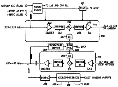
[0034] As shown in Fig. 2, the ODU (100) comprises a Block Up-Converter
(BUC) (200) and a Low Noise Block (LNB) (201). The BUC (200) performs
upconversion
of a signal to be transmitted. The LNB (201), on the other hand, receives a
signal transmitted
from a satellite, for example, and down converts the signal (reduces its
frequency) so that the
received signal can be demodulated and its data extracted. The LNB (201) down
converts the
received signal because the detection circuitry (not shown) is preferably
designed for lower
frequencies and cannot operate with signals of frequencies in the GHz range.
[0035] For example, in many two-way satellite communication systems, the LNB
(201) receives a signal of frequency fRx in the range of 19.7 GHz to 20.2 GHz
as shown in
Fig. 2. The LNB (201) down converts this signal to a frequency in the range of
950 MHz to
1450 MHz. The signal is then demodulated and down converted to baseband by the
detection
circuitry (not shown) where the data can be extracted from the signal.
[0036] The key components of the BUC (200), shown in Fig. 2, will now be
explained.
[0037] An input signal with frequency fIF enters the BUC (200) and is input
into a
driver circuit (202). The driver circuit (202) is shown in more detail in Fig.
3. As shown in
Fig. 3, the driver circuit (202) consists of a series of amplifiers (300) and
thermopads (301).
The amplifiers (300) amplify the input signal. The thermopads (301) compensate
for
changing temperature and keep the power output stable over temperature. The
theremopads
(301) provide power attenuation that varies with temperature, thus reducing
the variations in
the power of the signal.
7
CA 02492042 2005-01-06
WO 2004/006452 PCT/US2003/021864
[0038] Returning to Fig. 2, the signal output from the driver circuit (202) is
then
filtered with a filter (203) to remove the possible interference present at
unwanted frequencies
that would alias down and interfere with the desired signal during the
detection process.
[0039] The filtered signal is then mixed with a signal of frequency 3*fDRo
(where
* denotes inultiplication) using an analog mixer (204). This signal is derived
from the
Dielectric Resonance Oscillator Phase Lock Loop (DRO PLL) (208). The DRO PLL
(208)
will be explained in more detail below.
[00401 Using common trigonometric identities, it can be shown that the signal
output from the analog mixer (204) has a frequency fTX equal to 3*fDRo - f]F,
where fDRO is the
frequency of the output signal of the DRO PLL (208). In many two-way satellite
cominunication systems, fTx is in the range of 29.5 GHz to 30 GHz, as shown in
Fig. 2.
[0041] The analog mixer (204) output signal is then filtered with another
filter
(205) before being amplified with a power amplifier (PA) (206) designed to
amplify the
signal to the optimal output power level (e.g., 4 watts). After being
amplified by the PA
(206), the signal is fed into an anteima (102; Fig. 1) preferably via a
waveguide connector
(104; Fig. 1). The anteima (102; Fig. 1) then transmits the signal.
[0042] As shown in Fig. 2, a single DRO PLL (208) is preferably used to
implement the present invention. A reference signal of frequency fpEF is
generated in the IDU
(101; Fig.l) and sent to the ODU (100; Fig.1). Inside the ODU (100; Fig.1), a
band pass filter
(209) removes noise around this signal. The signal is then input into the DRO
PLL (208) as
its reference signal. The DRO PLL (208) generates a phase-locked signal (e.g.,
a sine wave)
of frequency fnRo. Different harmonics of this signal can be mixed with the
transmit IF signal
and the receive signal to obtain the desired output signals.
[0043] For example, in many two-way satellite communication systems, fPEF is
10.575 MHz. The output of the DRO PLL (208) is a phase-locked signal with fDRO
equal to
10.575 MHz. The third harmonic of this signal is obtained by multiplying the
signal by 3
using a multiplier (207). This signal is then mixed with the output of the
first BUC (200)
filter (203), as explained above, with an analog mixer (204) resulting in a
signal of frequency
fTx equal to 29.5 GHz to 30 GHz.
8
CA 02492042 2005-01-06
WO 2004/006452 PCT/US2003/021864
[0044] In the LNB (201), on the other hand, the second harmonic of the output
signal of the DRO PLL (208) is used to down convert the received signal from
the antenna
(102; Fig. 1) to a frequency of 950 MHz to 1450 MHz. The second harmonic is
obtained by
multiplying the output signal of the DRO PLL (208) by 2 using another
multiplier (210). This
signal is then mixed with the received signal from the antenna (102; Fig. 1)
using another
analog mixer (211).
[0045] As shown in Fig. 2, a microprocessor (212) is preferably used to
monitor
several status signals of the ODU (100; Fig. 1). Examples of signals to be
monitored include
the PLL Lock status output from the DRO PLL (208), Low DC Voltage status, and
the ODU
Controller status. The PLL Lock status indicates whether or not the output
signal of the DRO
PLL (208) is locked in phase. The low DC Voltage status monitors the DC
voltage to make
sure it is high enough for proper ODU (100; Fig.1) operation. The ODU
Controller status
indicates the health of the ODU (100; Fig.l) control electronics. If one of
these status signals
indicates an error in the ODU (100; Fig.1), the microprocessor (212) outputs a
signal, TX
Zs Mute, that stops the ODU (100; Fig.1) from transmitting by adjusting a bias
(214) that mutes
the PA (206).
[0046] The ODU (100; Fig.1) communicates the status signals to the IDU (101;
Fig. 1) so that the IDU (101; Fig. 1) circuitry can attempt to rectify the
problem. This
coinmunication is accomplished via a Digital Satellite Equipment Control
(DiSEqC) (213).
An exemplary DiSEqC (213) operates at 22 kHz and uses pulse width keying
(P)AK).
DiSEqC (213) messages are sent as sequences of short bursts of 22 kHz tones.
Each bit of
data occupies a specific time and the proportion of that tiine filled with the
22 kHz burst
determines whether that bit is a 1 or a 0.
[0047] Fig. 4 illustrates an embodiment of the present invention. The
embodiment entails a metliod and systein whereby the input signal power level
and the output
signal power level of the ODU (100; Fig. 1) are monitored by the
microprocessor (212) and
can be attenuated by a step attenuator (402) such that the output signal power
level becomes
equal to the maximum allowable power level. The embodiment will be explained
in more
detail below.
9
CA 02492042 2005-01-06
WO 2004/006452 PCT/US2003/021864
[0048] As shown in Fig. 4, the input and output signals of the ODU (100;
Fig.1)
are coupled to detectors (400a,b). A preferable detector (400a,b) outputs a
root-mean-square
(rms) DC voltage that is equivalent to the detected signal power level. The
detector (400a,b)
can be a circuit comprising discrete components such as diodes, resistors,
capacitors, and an
operational amplifier. The detector can also be an integrated circuit (IC)
chip, such as the
AD8361 detector made by Analog DevicesTM.
[0049] After the detectors (400a,b), analog to digital converters (A/Ds) (401
a,b)
digitize the output signals of the detectors (400a,b), as shown in Fig. 4.
Digitization is
performed because preferable microprocessors (212) function with digital
signal inputs. The
A/D (401a,b) outputs are then input into the microprocessor (212). Some
microprocessors
(212) have built in A/Ds and in this case, the external A/Ds would no longer
be needed.
[0050] The microprocessor (212) compares the digitized ODU (100; Fig.1) output
signal power level to a preset threshold. This preset threshold is preferably
equivalent to the
maximum allowable output signal power level. The threshold is programmable and
can be
varied.
[0051] If the ODU (100; Fig.1) output signal power level is above the
threshold,
the microprocessor (212) switches in a step attenuator (402) with a control
signal, ATT. The
control signal, ATT, preferably indicates to the step attenuator (402) the
amount of
attenuation necessary for the ODU (100; Fig.l) output power signal level to
equal the
threshold level.
[0052] The step attenuator (402) can be an IC or a circuit consisting of
discrete
components, for example. An exemplary step attenuator (402) has an attenuation
range of 15
dB with a 0.5 dB step resolution. The attenuation range and step resolution
can vary
depending on the specifications of the application.
[0053] The step attenuator (402) attenuates the ODU (100; Fig. 1) input signal
by
the amount specified by the control signal, ATT. This results in the
attenuation of the ODU
(100; Fig.1) output signal. This method and system of signal power attenuation
attenuates the
ODU (100; Fig.1) output signal power level without terminating the ODU (100;
Fig.1) output
signal. It is also faster than previous methods of attenuation where
communication with the
IDU (101; Fig. 1) is required because the use of a DiSEqC (213), which
currently operates at
CA 02492042 2005-01-06
WO 2004/006452 PCT/US2003/021864
relatively slow rates (e.g., 22 kHz), is not needed to attenuate the ODU (100;
Fig. 1) output
signal power level.
[0054] In a preferred embodiment, the settings of the step attenuator (402)
are sent
to the IDU (101; Fig.1) through the DiSEqC (213), as shown in Fig. 4, so that
the IDU (101;
Fig. 1) does not continue increasing the signal level at the ODU (100; Fig. 1)
input if the ODU
(100; Fig.1) output signal power level exceeds the threshold.
[0055] As previously explained, the ODU (100; Fig.1) input signal power level
is
also monitored by the microprocessor (212). The ODU (100; Fig.1) input signal
power level
is monitored for a variety of purposes including ODU (100; Fig. 1) fault
detection, fault
isolation, and initial gain setting at the IDU (101; Fig.1).
[0056] If the ODU (100; Fig. 1) output signal power level is still over the
threshold
level after the step attenuator (402) is set to its maximum attenuation level,
the
microprocessor (212) can preferably generate the signal, TX Mute, which mutes
the ODU
(100; Fig. 1) output signal using the bias (214) as explained previously.
[0057] The preceding description has been presented only to illustrate and
describe the invention. It is not intended to be exhaustive or to limit the
invention to any
precise form disclosed. Many modifications and variations are possible in
light of the above
teaching.
[0058] The preferred embodiment was chosen and described in order to best
explain the principles of the invention and its practical application. The
preceding description
is intended to enable others skilled in the art to best utilize the invention
in various
embodiments and with various modifications as are suited to the particular use
contemplated.
It is intended that the scope of the invention be defined by the following
claims.
11