Note: Descriptions are shown in the official language in which they were submitted.
CA 02492150 2005-O1-05
WO 2004/006459 PCT/US2003/021277
1
APPARATUS AND METHOD FOR RADIO FREQUENCY
TRACHING AND ACQUISITION
BACKGROUND
Technical Field
[0001] The present invention is related generally to radio frequency (RF)
reception
and, more specifically, to an apparatus and method for RF acquisition and
tracking.
Description of Related Art
[0002] Radio frequency (RF) receivers must be designed to acquire and track an
incoming RF signal. In an ideal environment, the RF signal travels from a
transmitter in a
direct line to the receiver. However, in a more realistic setting, the RF
signal from the
transmitter is reflected or diffracted by various objects and arnves at the RF
receiver along
multiple pathways. In such a multipath environment, the signal power level
fluctuates. In
RF receivers synchronization loops , such as phase-locked loops, have a loop
bandwidth
designed for operation at a desired operating point. However, in a multipath
environment,
the loop bandwidth of the synchronization loop varies as the signal power
level fluctuates.
In certain channel conditions, the variation can deviate significantly from
the designed
operating point, resulting in a performance loss, such as increased
acquisition time, smaller
pull-in/lock-in ranges, and the like. Conventional solutions to this problem
are increased
loop bandwidth design or the use of a hard limner or coherent automatic gain
control
(AGC) preceding the synchronization loop. However, each of these approaches
has design
limitations that, under realistic operating conditions, result in degraded
performance of the
RF receiver.
[0003] Therefore, it can be appreciated that there is a significant need for
an
apparatus and method that can optimize acquisition time and pull-in/lock-in
ranges even in
CA 02492150 2005-O1-05
WO 2004/006459 PCT/US2003/021277
2
a multipath environment. The present invention provides this and other
advantages as will
be apparent from the following detailed description and accompanying figures.
SUMMARY
[0004] The present invention is embodied in a system and method for the
detection
of a radio frequency signal. In one embodiment, the invention comprises an
apparatus for
the detection of a radio frequency (RF) signal and comprises a peak detector
to detect a
peak RF signal and to generate timing data and magnitude data related thereto.
A
despreader coupled to the peak detector receives the timing data therefrom and
despreads
the RF signal to generate a despread signal. A gain adjustment generator
coupled to the
peak detector receives magnitude data therefrom and generates a gain
adjustment factor
based on the magnitude data. A scaler scales the despread signal by the gain
adjustment
factor to generate an output signal.
[0005] In one embodiment, the peak detector is a noncoherent peak detector.
The
peak detector may comprise a noncoherent despreader, magnitude estimator and
sorter to
generate the timing and magnitude data.
[0006] In one embodiment, the gain adjustment generator calculates the gain
adjustment factor based on the magnitude data. Alternatively, the gain
adjustment generator
comprises a data storage area containing a plurality of gain adjustment
factors and a
selected one of the plurality of gain adjustment factors is selected as the
gain adjustment
factor based on the magnitude data. The data storage area may comprise a
lookup table
having an input based on the magnitude data and an output being the selected
one of the
plurality of gain adjustment factors.
[0007] In one embodiment, the scaler is implemented as a multiplier having
first
and second inputs. The first input is coupled to the despreader and the second
input is
coupled to the gain adjustment generator.
CA 02492150 2005-O1-05
WO 2004/006459 PCT/US2003/021277
3
[0008] In one embodiment, the apparatus further comprises a phase-locked loop
(PLL) comprising a phase detector, a filter, and a voltage-controlled
oscillator (VCO) or
numerically controlled oscillator (NCO) wherein the output signal is coupled
to the phase
detector. In one implementation of the PLL, the phase detector has first and
second inputs
and an output with the first input being configured to receive the output
signal and the
second input being coupled to an output of the VCO/NCO. The output of the
phase
detector is coupled to a control input of the VCO/NCO via the filter.
BRIEF DESCRIPTION OF THE DRAWINGS
[0009] FICZ 1 is a functional block diagram of a conventional phase-locked
loop.
[0010] FIO 2 is a functional block diagram of a conventional receiver using a
coherent automatic gain controller preceding a phase-locked loop.
[0011] FIG. 3 is a functional block diagram of a portion of a radio frequency
receiver illustrated in one implementation of the present invention.
[0012] FICA 4 is a flowchart illustrating the operation of one implementation
of the
present invention.
DETAILED DESCRIPTION OF THE EMBODIMENTS
[0013] Synchronization is an essential but challenging task performed in
communication receivers. For a receiver to reliability demodulate the
transmitted symbols,
accurate knowledge of the symbol timing (i.e., when a symbol starts and ends)
and carrier
frequency is necessary. In addition, coherent receivers must be able to
generate a reference
signal whose phase is synchronous with that of the received radio frequency
(RF) signal.
[0014] The most common synchronization technique is a phase-locked loop (PLL),
which is used for both earner phase and earner frequency recovery. A time-
tracking loop
CA 02492150 2005-O1-05
WO 2004/006459 PCT/US2003/021277
4
(TTL) is used for timing recovery. FICz 1 illustrates a conventional PLL 10.
As illustrated
in FICA 1, the PLL 10 is basically a feedback control system comprising three
basic
components: a phase detector 12, a loop filter 14, and a voltage-controlled
oscillator
(VCO) 16. Those skilled in the art will appreciate that the term VCO is
typically used in
analog circuits literature while the term numerically controlled oscillator
(NCO) is issued in
digital circuits literature. As used herein, the terms VCO and NCO can be used
interchangeably. The scope of the present invention is not limited by the
terms VCO and
NCO.
[0015] The phase detector 12 generates a signal indicative of the phase
difference
between an input signal (i.e., the RF signal) and the output of the VCO 16.
The signal from
the phase detector 12 is processed by the loop filter 14, which is typically a
low-pass filter
that removes high frequency components at the output of the phase detector 12.
Completing the loop, the output of the loop filter 14 is coupled to a control
input of the
VCO 16. The output of the VCO 16 is a phase estimate of the received signal
based on the
phase difference measured in the PLL 10.
[0016] A loop structure, similar to the PLL 10 illustrated in FIG l, is also
widely
used in frequency and symbol timing synchronization, such as automatic
frequency control
(AFC) and the TTL (which is an early-late gate synchronizer), respectively.
For example,
in the AFC loop, the phase detector 12 is replaced with a frequency detector
(not shown)
that measures the frequency difference between the received signal and the
output of the
VCO 16. In the TTL, the phase detector 12 is replaced with a discriminator
(not shown)
that produces a measure of timing error signal. The VCO 16 is replaced with a
voltage-
controlled clock (not shown) that indicates symbol timing. Thus, the basic
loop illustrated
by the PLL 10 in FIG. 1 can be modified in a known manner to provide the
desired signal
processing capability.
CA 02492150 2005-O1-05
WO 2004/006459 PCT/US2003/021277
[0017] The synchronization loop (e.g., the PLL 10, the AFC loop, and the TTL)
typically has two modes of operation, namely an acquisition mode, which
achieves
synchronization, and a tracking mode which maintains synchronization in the
presence of
unpredictable changes, such as those introduced by the propagation channel or
oscillator
drifts. Typically, designers are concerned with how fast the system acquires
synchronization and how reliably it maintains synchronization. As will be
discussed below,
these two goals (i.e., acquisition and tracking) are not compatible under all
circumstances.
Signal acquisition requires design considerations such as under what signal
conditions the
system can acquire. For example, the system design must consider the initial
frequency
offset between the received signal and the local oscillator that the system
can acquire. This
is sometimes referred to as the lock-in range of the receiver. In addition,
the receiver must
be designed to track changes, such as variations in signal strength, while
tracking the phase,
frequency and timing of the received signal.
[0018] An important parameter in loop design (e.g., a PLL, AFC, or TTL) is the
loop bandwidth, which is defined as the equivalent noise bandwidth of the
corresponding
closed-loop transfer function. For example, the loop bandwidth in the PLL 10
is the
equivalent noise bandwidth corresponding to the transfer function between the
phase of the
received signal and the phase of the output of the VCO 16. The loop bandwidth
depends on
characteristics of the three components illustrated in FIG 1. The
configuration of the loop
filter 14, such as the order of the filter and loop filter coefficients,
affect the bandwidth. In
addition, signal gains of the phase detector 12 and the VCO 16 and the input
signal level
also affect the loop bandwidth.
[0019] It is well known that, for a given external noise and interference
level, a
larger loop bandwidth allows more noise and interference to enter the loop,
resulting in
phase fitter (i.e., the phase estimate at the output of the VCO 16 is noisier)
and a lower loop
signal-to-noise ratio (SNR). For purposes of the present discussion, noise is
a background
CA 02492150 2005-O1-05
WO 2004/006459 PCT/US2003/021277
6
signal that may be present in the frequency band of interest and may be
manmade or
naturally occurnng. Interference, as used herein, refers to manmade signals,
such as
undesirable signals from microwaves, other base stations, and other wireless
communications systems. If the PLL 10 has a low SNR, the loop is more likely
to slip
cycles (i.e., incur phase error jumps by multiples of 2~c radians in a short
time interval),
which is detrimental to applications such as timing recovery. Under some
conditions, it is
possible to drop out of lock.
[0020] On the other hand, a wider loop bandwidth allows shorter acquisition
time
(i.e., the time needed to reach the synchronous state) and shorter loop
response time to
changes of the phase (or frequency or timing) of the received signal.
Furthermore, a loop
with a larger loop bandwidth has a larger pull-in/lock-in range, which is
defined as the
maximum frequency offset between the received signal and the free running
frequency of
the VCO 16 for which the loop can acquire with/without cycle slips. In
practice, the
designed operating point, such as the loop bandwidth, is determined by
balancing these
tradeoffs.
[0021] In a wireless mobile communication system, the transmitted signal
travels
through multiple propagation paths before arriving a the receiver. Since each
propagation
path causes random attenuation and phase offset, the received signal, which is
a
superposition of these multipath components, will experience variation in the
phase and
amplitude, as well as the arrival time due to the mobility of the receiver.
This fading
multipath effect may cause severe performance degradation if the receiver
design does not
mitigate these factors.
[0022] In a system employing direct-sequence spread-spectrum signaling, a RAKE
receiver is commonly used to combat the fading multipath effects. The RAKE
receiver
collects signal energies from multiple propagation paths and combines them to
increase
CA 02492150 2005-O1-05
WO 2004/006459 PCT/US2003/021277
7
SNR. RAKE receivers are well known in the art an need not be described in
greater detail
herein.
[0023] The effectiveness of the RAKE receiver is heavily dependent on the
accuracy of the channel estimate. In systems where an unmodulated pilot signal
is not
available, such as systems specified in the IEEE 802.11b standard, the channel
estimate is
typically obtained in a decision-directed manner. For example, correlating the
received
signal with a local replica of the spreading code at a given code offset gives
an estimate of
the product of the transmitted data symbol and the complex-valued channel gain
of the
multipath component at that offset (i.e., at the corresponding propagation
delay).
Therefore, assuming the decisions of the transmitted data symbols are
sufficiently reliable,
the estimate of the channel gain can be obtained by multiplying the
correlation by the
complex conjugate of the corresponding symbol decisions to remove the data
modulation.
Thus, this process is decision-directed. To obtain the most accurate symbol
decisions, it is
clear that, before the channel estimate is obtained and optimal combining can
take place,
the strongest multipath component should be used in the decision making
process since it
has the highest SNR among all multipath components.
[0024] It should be noted that timing, frequency, and/or phase synchronization
(using the various synchronization loops described above) are required to
accurately
demodulate the transmitted symbols. For the same reason discussed above with
respect to
the accuracy of the symbol decision, the strongest multipath component should
also be used
to drive the synchronization loops before multipath components can be
optimally
combined.
[0025] A design problem arises when the synchronization loops operate in a
multipath channel. As discussed above, for a given set of loop component
parameters and
configuration, the loop bandwidth depends on the signal power level entering
the loop (i.e.,
the input signal in FICx 1). Since the strengths of multipath components vary
over time in a
CA 02492150 2005-O1-05
WO 2004/006459 PCT/US2003/021277
8
random manner, the loop bandwidth, and hence the acquisition time and pull-
in/lock-in
ranges, fluctuate accordingly. This results in an amplitude modulation
phenomenon of the
loop bandwidth. That is, the loop bandwidth fluctuates with the amplitude of
the input
signal. When this fluctuation deviates significantly from the designed
operation point, the
system will experience a considerable performance loss.
[0026] For example, a typical communication receiver utilizes a noncoherent
automatic gain control (AGC) mechanism to keep the total input power of the
receiver (i.e.,
the sum of the signal, interference, and noise power) at a constant level.
However, in the
channel estimation process described above, only the strongest multipath
component can be
used to drive the synchronization loops. Therefore, even though the
noncoherent AGC
maintains a constant total received power, the distribution of the power of
the constituent
multipath components can vary over time. Thus, the strength of the strongest
multipath
signal can vary over time. This results in a variant input signal power into
the loop and thus
a variant loop bandwidth.
[0027] In a typical implementation, the loop parameters are designed based on
the
power levels set by the noncoherent AGC. In such a receiver design, the
resulting effective
loop bandwidth, which is dependent on the power level of the strongest path,
is smaller than
the target loop bandwidth, which is computed based on the total received
power.
Consequently, the receiver may have smaller pull-in and lock-in ranges and
therefore can
tolerate a smaller amount of frequency offset to acquire the input signal.
[0028] An additional consequence of the reduced loop bandwidth is a longer
acquisition time, assuming it can acquire at all, and therefore the reception
of short data
packets may fail. A mechanism must be provided that can compensate for the
loss of loop
bandwidth in a multipath environment to achieve better performance and
synchronization,
symbol decisions, channel estimation, and RAKE combining.
CA 02492150 2005-O1-05
WO 2004/006459 PCT/US2003/021277
9
[0029] Conventional attempts to alleviate this problem employ a wider loop
bandwidth or precede the synchronization loop with a hard limiter or a
coherent AGC.
Taking into account the attenuation due to the multipath effect, the bandwidth
widening
approach increases the target loop bandwidth based on the minimal acceptable
or average
signal strength of the strongest multipath component and uses this loop
bandwidth for all
possible incoming signal power levels. Since this approach is based on the
worst case or
average case scenario, the primary drawback is that the effective loop
bandwidth could be
excessive in certain channel conditions thereby allowing more noise to enter
the loop and
thus degrading the performance of the synchronization loop.
[0030] A hard limiter is essentially a two-level mid-riser scalar quantizer.
This
limiter outputs a positive constant value if the input is positive (or a
negative constant value
if the input is negative). This constant value is determined based on the
target loop
bandwidth. The hard limiter has a constant output power irrespective of the
input power
levels of the signal, noise, and interference. Thus, it is clear that the
presence of noise and
interference suppresses the signal power level at the output of the limner,
thereby degrading
the input SNR of the loop. This degradation exacerbates in low SNR conditions.
[0031] A conventional bandwidth adjustment scheme using a coherent AGC 20
preceding the PLL 10 is illustrated in the functional block diagram of FIG 2.
The coherent
AGC 20 has a feedback control structure similar to that of the PLL 10 of FIG.
1. The three
elements in the control loop are a gain control amplifier (GCA) 22, a
magnitude detector 24
and a filter 32. The magnitude detector 24 is similar to the phase detector 12
in FIG 1 in
that it compares two signals and generates a control voltage. While the phase
detector 12
compares the input signal with the output of the VCO 16, the magnitude
detector 24
compares a reference voltage VREF wlth the output of the GCA 22 and generates
a
difference signal. The difference signal is filtered by the filter 32 to
generate a control
signal for the GCA 22. The GCA 22 is used to adjust the power of the input
signal based on
CA 02492150 2005-O1-05
WO 2004/006459 PCT/US2003/021277
the control signal. The control signal to the GCA 22 is provided by the
magnitude detector
24 through the filter 32.
[0032) The output of the VCO 16 is coupled to a quadrature phase shifter 34 to
provide a phase reference signal for the magnitude detector 24, resulting in a
coherent
AGC. The magnitude detector 24 comprises a multiplier 26 and a low-pass filter
28. The
multiplier 26 combines the output of the GCA 22 and the phase reference signal
from the
quadrature phase shifter 34 to generate a measure of the signal magnitude. The
low-pass
filter 28 removes high frequency components of the product to provide a
magnitude
estimate. The output of the magnitude detector 24 is compared against the
reference
voltage VREF by an adder 30. The difference signal generated by the adder 30
is filtered by
the filter 32, the output of which serves as the control signal to adjust the
gain of the GCA
22.
[0033] Assuming the response of the coherent AGC 20 is sufficiently fast, it
can be
shown that the signal magnitude entering the PLL 10 is VnEF where the VREF is
the
cos 9e
reference voltage and 9e is the phase error between the input of the phase
detector 12 and
the output of the VCO 16. In a tracking mode (i.e., the PLL 10 is locked), Be
is close to
zero. Therefore, the input signal magnitude of the PLL 10 is held
approximately as a
constant at VREF, which corresponds to the desired operating point, such as
the target loop
bandwidth. However, in the acquisition mode (i.e., the PLL 10 is out of lock
and
attempting to acquire), 8e is not close to zero. As a result, the input signal
magnitude of the
PLL 10 is greater than VREF since the ~cos9e~<1 for 6e ~ k~c where k is an
integer, resulting in
an excessive loop bandwidth. The drawback of this approach is similar to that
of the
bandwidth widening approach discussed above. Appropriate adjustment of loop
bandwidth,
especially in the acquisition mode, is crucial to satisfactory operation of a
receiver circuit.
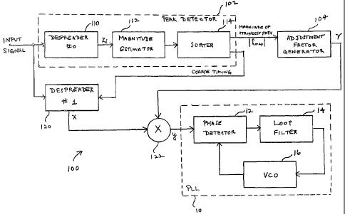
[0034] An embodiment of the present invention provides a technique by which
the
loop bandwidth is adjusted based on signal strength. An embodiment of the
present
CA 02492150 2005-O1-05
WO 2004/006459 PCT/US2003/021277
11
invention is shown in a system 100 illustrated in the functional block diagram
of FICx 3.
The system employs a noncoherent peak detector 102 to estimate the strength of
the
strongest multipath component and then scales the input of the synchronization
loop via a
bandwidth adjustment gain factor to compensate for the loss of loop bandwidth.
Since the
peak detector 102 is noncoherent, a phase reference from the synchronized PLL
10 is not
needed thereby alleviating the problem faced by the coherent AGC approach in
the
acquisition mode, as discussed above with respect to FIG 2. In addition, the
bandwidth
adjustment factor of the system 100 scales the signal component and the
interference/noise
component by the same amount. Therefore, unlike the hard limiter which causes
SNR
degradation, the input SNR of the loop in the system 100 is not changed. As
illustrated in
FIG 3, the input signal, which is the received signal, is a superposition of
all multipath
components, including interference and noise. The input signal is first
despread by a
despreader 110 at various code offsets. In a typical implementation, the
despreader 110
uses code offsets at every one-half chip interval. However, other intervals
may be used.
The present invention is not limited by the specific chip interval used by the
despreader
110.
[0035] For purposes of the following discussion, the complex-valued channel
gain
of the multipath component at the i'h code offset is designated as h; and the
gain associated
with the strongest multipath component is designated as h",~. Without a loss
of generality,
and for the convenience of exposition, it can be assumed that ~I hll2 =1. That
is, the
1
average received signal power is the same as the transmitted signal power. It
can also be
assumed, for the sake of discussion, that the transmitted data symbol d has a
unit power
(i.e., ~d~=1). Also, for the reasons discussed above, it can be assumed that
the local replica
of the spreading sequence at the receiver is normalized such that the output
of the
despreader 110 has a unit power when a transmitted spread sequence of a symbol
interval is
CA 02492150 2005-O1-05
WO 2004/006459 PCT/US2003/021277
12
received without any distortion. Thus, the output of the despreader 110 at the
i'h code offset
may be written as:
z~ =zlr +jzQ, =hid+1~ +Nl (1)
where z~r and zQ; are the in-phase and quadrature components of z"
respectively, and I;
and N; denote interference and noise of the i'h code offset, respectively. The
interference
may be from external sources and other multipath components.
[0036] Since the despreader 110 provides a processing gain that can suppress
noise
and interference (i.e., 1; and N; in equation (1) are relatively small
compared to the signal
component h; and ci7, it follows that z; serves as an estimate of the product
of the transmitted
data symbol d and channel gain h;.
[0037] The outputs {z;} of the despreader 110 are coupled to a magnitude
estimator
112, which generates the magnitude estimates of the channel gains of the
various multipath
components. The magnitude estimator 112 can be implemented with a variety of
different
techniques. For example, the magnitude estimate of h;, denoted as ~~;~, may be
obtained
noncoherently by:
Ih~I=Iz1(= z112+zQi2 ~~h~~~d~_~h~~
where it has been assumed that ~d~=1. Those skilled in the art will recognize
that the
magnitude estimator 112 may be implemented using other known techniques. The
present
invention is not limited by the specific implementation of the magnitude
estimator 112.
[0038] It should be noted that the magnitude estimates are typically averaged
over
several symbol intervals to reduce the variance of the estimates. These
magnitude estimates
are coupled to a sorter 114 that selects the largest magnitude,
denoted by ~~",~~ where:
CA 02492150 2005-O1-05
WO 2004/006459 PCT/US2003/021277
13
hmax ( - m~ ~ ( hi
where the value of I h,n~ I represents the magnitude estimate of the strongest
multipath
component and the corresponding code phase indicates the coarse timing of that
multipath
component. That is, the i'h code offset provides timing information while the
magnitude
associated with that i'" component is given by equation (3) above. Thus, the
sorter 114
produces both magnitude and timing information. The magnitude of the strongest
path (i.e.,
~~",~~) indicates the magnitude of the strongest path. The signal is provided
to an
adjustment factor generator 104, as will be described in greater detail below.
[0039] As noted above, the sorter 114 also produces coarse timing information
indicative of the timing of the strongest path of the multipath components.
The coarse
timing information is used in a despreader 120 to despread the strongest
multipath
component. Similar to the output of the despreader 110 as expressed in
equation (1), it
clear that the output of the despreader 120 can be expressed as:
x = h",~d + I' + N' (4)
where I' and N' denote the corresponding interference and noise components,
respectively.
It should be noted that fine timing for the strongest signal path may be
derived by a TTL
(not shown) and used together with the coarse timing for the despreader 120.
For the sake
of brevity and clarity, the fine timing component is not illustrated in FIG 3.
However, the
use of a TTL for fine timing is well known in the art, and need not be
described in greater
detail herein.
[0040] It should be noted that, in a typical design, the output of the
despreader 120
(designated as x), is the input of the synchronization loop. This is the
equivalent of the
"Input Signal" in FIGs. I-2. As previously discussed with respect to a
noncoherent AGC,
the loop bandwidth parameter is typically designed based on the total received
power
CA 02492150 2005-O1-05
WO 2004/006459 PCT/US2003/021277
14
maintained by the noncoherent AGC. That is, the desired input of the loop can
be
expressed as:
'desired = ~,I hi I2d '~" I -I- N = d ~- I -t- N (S)
i
where all parameters have been previously defined. Note that in equation (5),
the term
~I hl l2 represents the total received power collected from all the multipath
components
i
with the assumption that the noncoherent AGC achieves ~I hl I2 =1. Comparing
i
equations (4) and (5), it can be seen that x, the input of the synchronization
loop, is
attenuated by h",~ since h"Z~ < ~I hl I2 =1, resulting in a loss of loop
bandwidth.
[0041] To compensate for the loss of loop bandwidth, the output of the
despreader
120 is scaled by a factor y = 1 using, by way of example, a multiplier. This
factor is
hmax
computed based on the magnitude of the strongest path (i.e., ~~",~~) of the
output of the peak
detector 102, such that the output of the multiplier 122, designated as y in
FIG 3, becomes:
1 x = hmax d + I~+N~ = d ~, I~+N~ (6)
hmax I I hmax I I hmax I I hmax
where the approximation that ~h",~~~~h",~~ follows from equation (2) above.
Comparing
equation (5) with equation (6), it is clear that, after gain adjustment, the
input signal power
is approximately the same as the desired one.
[0042] For efficient hardware implementation, the generation of the loop
bandwidth
adjustment factor by the adjustment factor 104 can be obtained by a table look-
up to
eliminate the division operation required in computing y = I Specifically, the
input
hmax .
CA 02492150 2005-O1-05
WO 2004/006459 PCT/US2003/021277
of the data look-up table is the peak detector output ~~",~~, and the output
of the table is pre-
1
computed quantized version of
hmax ( .
[0043] It should be noted that multiple ways of performing the quantization
may be
implemented by the system 100. For example, the quantization may be linear or
nonlinear.
The actual implementation depends on the specific performance requirement and
the
complexity constraints, such as the maximum memory size allowed to store the
lookup
table. It is further noted that the multiplication of the adjustment factor by
the multiplier
122 can be done after the phase detector 12 and before the loop filter 14. In
this manner, it
is possible to save a real multiplier because the output of the despreader 120
is typically
complex-valued while the output of the phase detector 12 is real-valued.
Finally, it should
be noted that although FIG 3 is illustrated with the use of the PLL 10, the
same loop
adjustment mechanism can be applied without modification to the AFC and the
TTL simply
by replacing the PLL in FIG 3 by the corresponding synchronization loop.
[0044] The components illustrated in the functional block diagram of FIG 3 may
be
implemented by known hardware components or implemented as a set of
instructions
executed by a processor, such as a digital signal processor (DSP).
Alternatively, the
components illustrated in the functional block diagram of FIG 3 may be
implemented by a
combination of hardware components and instructions executed by the DSP.
[0045] The process implemented by the system 100 is illustrated in the
flowchart of
FIG 4 where at a start 200 an input signal has been detected by a radio
receiver. Those
skilled in the art will appreciate that conventional radio components, such as
an antenna,
radio frequency amplifier, filters, and the like may be used with the system
100. For the
sake of clarity and brevity, these conventional components are not illustrated
herein. In step
202, the system 100 despreads the incoming signal at selected code intervals.
Although a
typical code interval of one-half chip may be used, other code intervals may
be readily
implemented by the system 100. In step 204, the system 100 determines the
maximum
CA 02492150 2005-O1-05
WO 2004/006459 PCT/US2003/021277
16
magnitude and timing. As previously discussed, a series of code samples at the
selected
chip intervals are analyzed to determine which code interval has the maximum
amplitude.
The magnitude of that sample and the timing of that sample are used in
subsequence
processes.
[0046] In step 206, the system 100 uses the maximum magnitude to determine an
adjustment factor. As previously discussed, the adjustment factor may be
calculated in real
time based on the teachings provided herein. Alternatively, the calculations
may be
performed in advance with desired scale factors prestored in a storage area,
such as a look-
up table. Different implementations of the storage area are known in the art
and need not
be described herein. The present invention is not limited by the specific
implementation of
the adjustment factor, whether it is implemented in the form of real time
calculations, data
look-up table, or whether it is implemented by hardware or software
instructions executed
by the DSP.
[0047] In step 208, the system 100 uses the timing information derived in step
204
to despread the incoming signal. As previously discussed, the selected code
sample may
provide rough timing information and a TTL may be used to provide fine timing
information for the despreading operation performed in step 208. In step 210,
the system
scales the despread signal based on the adjustment factor calculated in step
206.
[0048] In step 212, the system 100 provides the scaled signal to a phase
locked
loop, such as the PLL 10 in FIG 3. The process ends at step 214.
[0049] Thus, the system 100 scales the input signal to achieve the desired
loop
bandwidth in the PLL 10. The system 100 has been described above in a number
of
varying implementations. It is to be understood that even though the various
embodiments
and advantages have been set forth in the foregoing description, the above
disclosure is
illustrative only, and changes may be made in detail, yet remain within the
broad principles
CA 02492150 2005-O1-05
WO 2004/006459 PCT/US2003/021277
17
of the invention. Therefore, the present invention is to be limited only by
the appended
claims.
[0050] All of the above U.S. patents, U.S. patent application publications,
U.S.
patent applications, foreign patents, foreign patent applications and non-
patent publications
referred to in this specification and/or listed in the Application Data Sheet,
are incorporated
herein by reference, in their entirety.
What is claimed is: