Note: Descriptions are shown in the official language in which they were submitted.
CA 02492689 2005-O1-18
WO 2004/006352 PCT/US2003/021617
TITLE
ELECTRONIC DEVICES MADE WITH
ELECTRON TRANSPORT AND/OR ANTI-QUENCHING LAYERS
BACKGROUND OF THE INVENTION
Cross Reference to Related Applications
This application claims priority from U.S. Provisional Application
Serial No. 60/394767, filed July 10, 2002, and U.S. Provisional Application
Serial No. 60/458277, filed March 28, 2003.
Field of the Invention
The present invention relates to photoactive electronic devices in
which there is at least one active layer comprising an electron transport
and/or anti-quenching composition.
Description of the Related Art
In organic photoactive electronic devices, such as light-emitting
diodes ("OLED"), that make up OLED displays, the organic active layer is
sandwiched between two electrical contact layers in an OLED display. In
an OLED the organic photoactive layer emits light through the light-
transmitting electrical contact layer upon application of a voltage across
the electrical contact layers.
It is well known to use organic electroluminescent compounds as
the active component in light-emitting diodes. Simple organic molecules,
conjugated polymers, and organometallic complexes have been used.
Devices which use photoactive materials, frequently include one or
more charge transport layers, which are positioned between the
photoactive (e.g., light-emitting) layer and one of the contact layers. A
hole transport layer may be positioned between the photoactive layer and
the hole-injecting contact layer, also called the anode. An electron
transport layer may be positioned between the photoactive layer and the
electron-injecting contact layer, also called the cathode.
When organometallic compounds, such as Ir and Pt complexes, are
used as the electroluminescent layer, a blocking layer inserted next to the
luminescent layer on the cathode side can enhance the device efficiency.
2,9-Dimethyl-4,7-diphenyl-1,10-phenanthroline (known as BCP or DDPA)
was used by Baldo et al. for this purpose. It was proposed that the BCP
layer functions as an "exciton blocker" to prevent the transfer of the energy
of a luminescent exciton to the adjacent layer. The blocking layer is
characterized by a band gap greater than the energy level of excitons
formed in the luminescent layer.
1
CA 02492689 2005-O1-18
WO 2004/006352 PCT/US2003/021617
US 6,097,147 claims a light emitting device comprising: a
substantially transparent anode; a hole transporting layer over said anode;
an emission layer over said hole transporting layer; a blocking layer over
said emission layer; an electron transporting layer over said blocking layer;
and a cathode in electrical contact with said electron transporting layer. It
further claims a device wherein said blocking layer is characterized by a
band gap greater than the energy level of excitons formed in said emission
layer.
However, energy transfer from photoactive materials to an adjacent
layer can be quenched not only by energy transfer but also by electron
transfer to the adjacent layer, so the use of larger band gap exciton
blocker is insufficient. Materials that can prevent both energy transfer
quenching and electron transfer quenching are needed.
SUMMARY OF THE INVENTION
The present invention is directed to a photoactive device
comprising an anode, a cathode, and a photoactive layer, which device
further comprises an electron transport and/or anti-quenching layer which
minimizes both electron transfer quenching and energy transfer quenching
of the photoactive layer.
In one embodiment is a photoactive electronic device comprising:
(a) an anode;
(b) a cathode, said cathode having a work function energy level E3;
(c) a photoactive layer positioned between said anode and said
cathode, said photoactive layer comprising a cyclometallated complex of a
transition metal, said cyclometalated complex having a LUMO energy level
E~ and a HOMO energy level E4; and
(d) an electron transport andlor anti-quenching layer positioned
between said cathode and said photoactive layer, said electron transport
and/or anti-quenching layer having a LUMO energy level Eland a HOMO
energy level E5,
with the proviso that:
(1) El - Eg 1V
(2) El - E2 > -1V, and
(3) E4 - E5 > -1 V.
As used herein, the term "charge transport composition" is intended
to mean material that can receive a charge from an electrode and
facilitates movement through the thickness of the material with relatively
high efficiency and small loss of charge. Hole transport compositions are
2
CA 02492689 2005-O1-18
WO 2004/006352 PCT/US2003/021617
capable of receiving a positive charge from an anode and transporting it.
Electron transport compositions are capable of receiving a negative
charge from a cathode and transporting it. The term "anti-quenching
composition" is intended to mean a material which prevents, retards, or
diminishes both the transfer of energy and the transfer of an electron to/or
from the excited state of the photoactive layer to an adjacent layer. The
term "photoactive" refers to any material that exhibits electroluminescence,
photoluminescence, and/or photosensitivity. The term "HOMO" refers to
the highest occupied molecular orbital of a compound. The term "LUMO"
refers to the lowest unoccupied molecular orbital of a compound. The
term "group" is intended to mean a part of a compound, such as a
substituent in an organic compound. The prefix "hetero" indicates that one
or more carbon atoms has been replaced with a different atom. The term
"alkyl" is intended to mean a group derived from an aliphatic hydrocarbon
having one point of attachment, which group may be unsubstituted or
substituted. The term "heteroalkyl" is intended to mean a group derived
from an aliphatic hydrocarbon having at least one heteroatom and having
one point of attachment, which group may be unsubstituted or substituted.
The term "alkylene" is intended to mean a group derived from an aliphatic
hydrocarbon and having two or more points of attachment. The term
"heteroalkylene" is intended to mean a group derived from an aliphatic
hydrocarbon having at least one heteroatom and having two or more
points of attachment. The term "alkenyl" is intended to mean a group
derived from a hydrocarbon having one or more carbon-carbon double
~5 bonds and having one point of attachment, which group may be
unsubstituted or substituted. The term "alkynyl" is intended to mean a
group derived from a hydrocarbon having one or more carbon-carbon
triple bonds and having one point of attachment, which group may be
unsubstituted or substituted. The term "alkenylene" is intended to mean a
group derived from a hydrocarbon having one or more carbon-carbon
double bonds and having two or more points of attachment, which group
may be unsubstituted or substituted. The term "alkynylene" is intended to
mean a group derived from a hydrocarbon having one or more carbon-
carbon triple bonds and having two or more points of attachment, which
group may be unsubstituted or substituted. The terms "heteroalkenyl",
"heteroalkenylene", "heteroalkynyl" and "heteroalkynlene" are intended to
mean analogous groups having one or more heteroatoms. The term "aryl"
is intended to mean a group derived from an aromatic hydrocarbon having
3
CA 02492689 2005-O1-18
WO 2004/006352 PCT/US2003/021617
one point of attachment, which group may be unsubstituted or substituted.
The term "heteroaryl" is intended to mean a group derived from an
aromatic group having at least one heteroatom and having one point of
attachment, which group may be unsubstituted or substituted. The term
"arylalkylene" is intended to mean a group derived from an alkyl group
having an aryl substituent, which group may be further unsubstituted or
substituted. The term "heteroarylalkylene" is intended to mean a group
derived from an alkyl group having a heteroaryl.substituent, which group
may be further unsubstituted or substituted. The term "arylene" is
intended to mean a group derived from an aromatic hydrocarbon having
two points of attachment, which group may be unsubstituted or
substituted. The term "heteroarylene" is intended to mean a group derived
from an aromatic group having at least one heteroatom and having two
points of attachment, which group may be unsubstituted or substituted.
The term "arylenealkylene" is intended to mean a group having both aryl
and alkyl groups and having one point of attachment on an aryl group and
one point of attachment on an alkyl group. The term
"heteroarylenealkylene" is intended to mean a group having both aryl and
alkyl groups and having one point of attachment on an aryl group and one
point of attachment on an alkyl group, and in which there is at least one
heteroatom. Unless otherwise indicated, all groups can be unsubstituted
or substituted. The phrase "adjacent to," when used to refer to layers in a
device, does not necessarily mean that one layer is immediately next to
another layer. On the other hand, the phrase "adjacent R groups," is used
to refer to R groups that are next to each other in a chemical formula (i.e.,
R groups that are on atoms joined by a bond). The term "compound" is
intended to mean an electrically uncharged substance made up of
molecules that further consist of atoms, wherein the atoms cannot be
separated by physical means. The term "ligand" is intended to mean a
molecule, ion, or atom that is attached to the coordination sphere of a
metallic ion. The term "complex", when used as a noun, is intended to
mean a compound having at least one metallic ion and at least one ligand.
The term "cyclometallated complex" is intended to mean a complex in
which an organic ligand is bound to a metal in at least two positions to
form a cyclic metal ligand structure, and in which at least one point of
attachment is a metal-carbon bond. In addition, the IUPAC numbering
system is used throughout, where the groups from the Periodic Table are
4
CA 02492689 2005-O1-18
WO 2004/006352 PCT/US2003/021617
numbered from left to right as 1 through 18 (CRC Handbook of Chemistry
and Physics, 81St Edition, 2000).
Unless otherwise defined, all technical and scientific terms used
herein have the same meaning as commonly understood by one of
ordinary skill in the art to which this invention belongs. Unless otherwise
defined, all letter symbols in the figures represent atoms with that atomic
abbreviation. Although methods and materials similar or equivalent to
those described herein can be used in the practice or testing of the
present invention, suitable methods and materials are described below.
All publications, patent applications, patents, and other references
mentioned herein are incorporated by reference in their entirety. In case
of conflict, the present specification, including definitions, will control.
In
addition, the materials, methods, and examples are illustrative only and
not intended to be limiting.
Other features and advantages of the invention will be apparent
from the following detailed description, and from the claims.
DESCRIPTION OF THE DRAWINGS
Figure 1 is a schematic diagram of a light-emitting diode (LED).
Figure 2 is a schematic diagram of the energy levels in an LED.
Figure 3 shows Formulae I(a) through I(e) for electroluminescent
iridium complexes.
Figure 4 shows Formula II for an electron transport composition.
Figure 5 shows Formulae II(a) through II(i) for an electron transport
composition.
Figure 6 shows Formulae III(a) and III(b) for an electron transport
composition.
Figure 7 shows Formulae IV(a) through IV(h) for a multidentate
linking group.
Figure 8 shows Formula IV for an electron transport composition.
Figure 9 shows Formulae IV(a) through IV(ag) for an electron
transport composition.
Figure 10 shows Formula shows Formula VI for an electron
transport composition.
Figure 11 shows Formulae VI(a) through VI(m) for an electron
transport composition.
Figure 12 shows Formula VII for an electron transport composition.
Figure 13 shows formulae for known electron transport
compositions.
5
CA 02492689 2005-O1-18
WO 2004/006352 PCT/US2003/021617
Figure 14 is a schematic diagram of a testing device for an LED.
Figure 15 is a diagram of EL efficiency for devices using iridium
complex I(a).
Figure 16 is a diagram of EL efficiency for devices using iridium
complex I(b).
Figure 17 is a plot showing the best ET/AQ compositions for
different iridium complex emitters. '
Figure 18 is a plot of the LUMO of the iridium complex emitters vs
the LUMO of ET/AQ compositions.
DETAILED DESCRIPTION OF THE PREFERRED EMBODIMENTS
The present invention relates to an electronic device comprising at
least one electron transport and/or anti-quenching layer and a photoactive
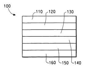
layer positioned between two electrodes. The device 100, shown in
Figure 1, has an anode layer 110 and a cathode layer 160. Adjacent to
the anode is a layer 120 comprising hole transport material. Adjacent to
the cathode is a layer 140 comprising an electron transport and/or anti-
quenching material. Between the hole transport layer and the electron
transport and/or anti-quenching layer is the photoactive layer 130. As an
option, devices frequently use another electron transport layer 150, next to
the cathode. Layers 120, 130, 140, and 150 are individually and
collectively referred to as the active layers.
Depending upon the application of the device 100, the photoactive
layer 130 can be a light-emitting layer that is activated by an applied
voltage (such as in a light-emitting diode or light-emitting electrochemical
cell), a layer of material that responds to radiant energy and generates a
signal with or without an applied bias voltage (such as in a photodetector).
Examples of photodetectors include photoconductive cells, photoresistors,
photoswitches, phototransistors, and phototubes, and photovoltaic cells,
as these terms are described in Markus, John, Electronics and Nucleonics
Dictionary, 470 and 476 (McGraw-Hill, Inc. 1966). A device within the
scope of this invention shall mean a light-emitting diode, light-emitting
electroluminescent device, or a photodetector as defined above.
Figure 2 shows the schematics of the energetics of the devices,
which will be used for the discussion below. All of the energy levels are
referenced to the vacuum level, 117, with an energy defined to be zero. As
such, they are all negative numbers. The lowest un-occupied molecular
orbital (LUMO) energy level of the ET/AQ layer is defined as E~. The
6
CA 02492689 2005-O1-18
WO 2004/006352 PCT/US2003/021617
LUMO of the photoactive layer is defined as E2. The work function of the
cathode is defined as E3, the highest occupied molecular orbital (HOMO)
of the photoactive layer is defined as E4, and the HOMO of the ET/AQ
layer is defined as E5. Higher energy means the energy level is closer to
the vacuum level. These energy levels can be measured in the solid state
by techniques such as photoelectron spectroscopy. One can also use
cyclic voltammetry measurement in solution to measure the relative
energy levels of the molecule.
An effective electron transport and/or anti-quenching (ET/AQ)
material in an electroluminescent device has to possess the following
properties.
1. The material has to be able to transport electrons efficiently,
preferably with a mobility of > 10-7 cm2/(V~sec).
2. The energy difference between the LUMO of the ET/AQ material
and the work function of the cathode has to be small enough to allow
efficient electron injection from the cathode. The energy barrier is
preferred to be less than 1 V, that is , E~-E3<1 V
3. The LUMO level of ET/AQ has to be high enough to prevent it
from receiving an electron from the photoactive layer. This usually requires
E~-E2>-1V. Preferably, E~-E2>0.
4. The HOMO level of ET/AQ has to be low enough to prevent it
from donating an electron to the photoactive layer. This usually requires
E4-E5>-1 V. Preferably, E4-E5>0.
Optimal energy level of ET/AQ in criteria 3 and 4 described above
can be determined by the application of electron transfer theory. The rate
of electron transfer reaction as a function of the energy difference is
described by the Marcus theory. (R. A. Marcus, P. Siders, J. Phys. Chem.,
86, 622(1982). In its simplest form, it is written as
k=vexp[-(Ef-E;+~,)2/4~,kBT]
(1 )
Here, k is the rate constant, kB the Boltzman constant, T the temperature,
Ei and Ef are the energies of the initial and final states, and ~, called the
reorganization energy, is a phenomenological parameter describing the
collective effects of the vibronic interactions in the initial and final
states.
The pre-factor v involves wave function overlap integrals, a, and is
7
CA 02492689 2005-O1-18
WO 2004/006352 PCT/US2003/021617
phenomenologically characterized as depending on the charge separation
distance r via
v(r) = vo exp [-a(r-ro)]
(2)
The prefactor vo tends to be universally about 1013 sec 1.
The energy of the final state, that is, the charge separated state,
depends on the separation distance of the electron and hole, r, as well as
the applied electric field, Eo. It can be written as
Et = Ef~ _ e2/(sr) _ Eoz
(3)
where Ef~ is the energy of the charge separated state in the absence of an
external field and with infinite separation of the electron and hole, s is the
dielectric constant of the medium, and z is the direction of the applied
field.
How to calculate the electron transfer rate under applied field and variable
electron hole distance has been discussed before by Wang and Suna,
J.Phys.Chem., 101, 5627-5638(1997).
In criteria 3, to prevent significant electron transfer quenching to
occur, the LUMO level of the ETIAQ layer has to be high enough such that
the electron transfer rate from the photoactive layer to the ET/AQ layer is
significantly less than the excited state radiative decay rate of the exciton.
So the optimal location of the LUMO level depends on the reorganization
energy ~, and overlap integral a of the electron transfer reaction involved,
and the radiative lifetime of the exciton of the photoactive layer. Typically,
this requires E~-E2>-1V. Preferably, E~-E2>0.
In criteria 4, similarly, the HOMO level of the ET/AQ layer has to be
low enough such that the electron transfer rate from the ET/AQ layer to
the luminescent layer is significantly less than the excited state radiative
decay rate of the exciton. The optimal location of the HOMO level
depends on the reorganization energy ~, and overlap integral a of the
electron transfer reaction involved, and the radiative lifetime of the exciton
of the photoactive layer. This usually requires E4-E5>-1V. Preferably, E4-
E5>0.
For any given photoactive material, there is therefore an optimal
ET/AQ material to use which fulfills the requirement outlined in criteria 1 to
8
CA 02492689 2005-O1-18
WO 2004/006352 PCT/US2003/021617
4. For a series of structurally similar ET/AQ materials, where the
reorganization energy and overlap integral are expected to be similar, one
expects to find a correlation between the efficiency of the device and the
LUMO energy of the ET/AQ material. For a given photoactive material,
there should be an optimal range of the LUMO energies of ET/AQ material
where the maximal efficiency is achieved.
It is also to be understood that the ET/AQ material has to be
chemically compatible with the photoactive material used. For example,
the ET/AQ material has to form a smooth film when deposited on the
photoactive material layer. If aggregation occurs, the performance of the
device will deteriorate. The occurrence of aggregation can be detected by
various known techniques in microscopy and spectroscopy.
The other layers in the device can be made of any materials which
are known to be useful in such layers. The anode 110, is an electrode that
is particularly efficient for injecting positive charge carriers. It can be
made
of, for example materials containing a metal, mixed metal, alloy, metal
oxide or mixed-metal oxide, or it can be a conducting polymer, and
mixtures thereof. Suitable metals include the Group 11 metals, the metals
in Groups 4, 5, and 6, and the Group 8-10 transition metals. If the anode
is to be light-transmitting, mixed-metal oxides of Groups 12, 13 and 14
metals, such as indium-tin-oxide, are generally used. The anode 110 may
also comprise an organic material such as polyaniline as described in
"Flexible light-emitting diodes made from soluble conducting polymer,"
Nature vol. 357, pp 477-479 (11 June 1992). At least one of the anode
and cathode should be at least partially transparent to allow the generated
light to be observed.
Examples of hole transport materials which may be used for layer
120 have been summarized, for example, in Kirk-Othmer Encyclopedia of
Chemical Technology, Fourth Edition, Vol. 18, p. 837-860, 1996, by Y.
Wang. Both hole transporting molecules and polymers can be used. The
compound bis(4-N,N-diethylamino-2-methylphenyl)-4-
methylphenylmethane (MPMP) has been disclosed to be a suitable hole
transport composition in Petrov et al., Published PCT application WO
02/02714. Commonly used hole transporting molecules are:
N,N'-diphenyl-N,N'-bis(3-methylphenyl)-[1,1'-biphenyl]-4,4'-diamine (TPD),
1,1-bis[(di-4-tolylamino) phenyl]cyclohexane (TAPC), N,N'-bis(4-
methylphenyl)-N,N'-bis(4-ethylphenyl)-[1,1'-(3,3'-dimethyl)biphenyl]-4,4'-
diamine (ETPD), tetrakis-(3-methylphenyl)-N,N,N',N'-2,5-
9
CA 02492689 2005-O1-18
WO 2004/006352 PCT/US2003/021617
phenylenediamine (PDA), a-phenyl-4-N,N-diphenylaminostyrene (TPS),
p-(diethylamino)benzaldehyde diphenylhydrazone (DEH), triphenylamine
(TPA), bis[4-(N,N-diethylamino)-2-methylphenyl](4-methylphenyl)methane
(MPMP), 1-phenyl-3-[p-(diethylamino)styryl]-5-[p-(diethylamino)phenyl]
pyrazoline (PPR or DEASP), 1,2-trans-bis(9H-carbazol-9-yl)cyclobutane
(DCZB), N,N,N',N'-tetrakis(4-methylphenyl)-(1,1'-biphenyl)-4,4'-diamine
(TTB), and porphyrinic compounds, such as copper phthalocyanine.
Commonly used hole transporting polymers are polyvinylcarbazole,
(phenylmethyl)polysilane, and polyaniline and mixtures thereof. It is also
possible to obtain hole transporting polymers by doping hole transporting
molecules such as those mentioned above into polymers such as
polystyrene and polycarbonate.
Examples of the photoactive layer 130 include all known
electroluminescent materials. Organometallic electroluminescent
compounds are preferred. The most preferred compounds include
cyclometalated iridium and platinum electroluminescent compounds and
mixtures thereof. Complexes of Iridium with phenylpyridine,
phenylquinoline, or phenylpyrimidine ligands have been disclosed as
electroluminescent compounds in Petrov et al., Published PCT Application
WO 02/02714. Other organometallic complexes have been described in,
for example, published applications US 2001/0019782, EP 1191612, WO
02/15645, and EP 1191614. Electroluminescent devices with an active
layer of polyvinyl carbazole (PVK) doped with metallic complexes of
iridium have been described by Burrows and Thompson in published PCT
applications WO 00/70655 and WO 01/41512. Electroluminescent
emissive layers comprising a charge carrying host material and a
phosphorescent platinum complex have been described by Thompson et
al., in U.S. Patent 6,303,238, Bradley et al., in Synth. Met. (2001 ), 116 (1-
3), 379-383, and Campbell et al., in Phys. Rev. B, Vol. 65 085210. as have
been Examples of a few suitable iridium complexes are given in Figure 3,
as Formulae I(a) through I(e). Analogous tetradentate platinum
complexes can also be used. These electroluminescent complexes can
be used alone, or doped into charge-carrying hosts, as noted above.
One type of ET/AQ material is a phenanthroline derivative. The
phenanthroline derivative can have Formula II, shown in Figure 4,
wherein:
CA 02492689 2005-O1-18
WO 2004/006352 PCT/US2003/021617
R1 and R2 are the same or different at each occurrence and are
selected from H, F, CI, Br, alkyl, heteroalkyl, alkenyl, alkynyl,
aryl, heteroaryl, CnHaFb, OCnHaFb, CgHcFd, and OCgHcFd;
a, b, c, and d are 0 or an integer such that a+b = 2n + 1, and c + d =
5,
n is an integer;
x is 0 or an integer from 1 through 3;
y is 0, 1 or 2;
with the proviso that there is at least one substituent on an aromatic
group selected from F, CnHaFb, OCnHaFb, CgHcFd, and OCgHcFd.
Specific examples of such phenanthrolines are Formulae II(a) through II(i)
in Figure 5.
The phenanthroline derivative can have Formulae III(a) or II(b),
shown in Figure 6, wherein:
R1, R2, a through d, n and x are as defined above;
R3 is the same or different at each occurrence and is selected from
a single bond and a group selected from alkylene,
heteroalkylene, arylene, heteroarylene, arylenealkylene, and
heteroarylenealkylene;
Q is selected from a single bond and a multivalent group;
m is an integer equal to at least 2; and
pis0or1.
Examples of multivalent Q groups are shown as Formulae IV(a) through
IV(h) in Figure 7.
Another type of ET/AQ material is a quinoxaline derivative. The
quinoxaline derivative can have Formula V, shown in Figure 8, wherein:
R4 and R5 are the same or different at each occurrence and are
selected from H, F, CI, Br, alkyl, heteroalkyl, alkenyl, alkynyl,
aryl, heteroaryl, alkylenearyl, alkenylaryl, alkynylaryl,
alkyleneheteroaryl, alkenylheteroaryl,
alkynylheteroaryI,CnHaFb, OCnHaFb, CgHcFd, and OCgHcFd,
or both of R5 together may constitute an arylene or
heteroarylene group;
a, b, c, and d are 0 or an integer such that a+b = 2n + 1, and c + d
= 5,
n is an integer, and
w is 0 or an integer from 1 through 4.
11
CA 02492689 2005-O1-18
WO 2004/006352 PCT/US2003/021617
Specific examples of quinoxalines of this formula are given as Formulae
V(a) through V(ag) in Figure 9.
The quinoxaline can have Formula VI, shown in Figure 10, wherein:
R4, R5, a through d, and n are as defined above,
R3 is the same or different at each occurrence and is selected from
a single bond and a group selected from alkylene,
heteroalkylene, arylene, heteroarylene, arylenealkylene, and
heteroarylenealkylene;
Q is selected from a single bond and a multivalent group;
m is an integer equal to at least 2;
pis0or1;and
w is 0 or an integer from 1 through 4.
Examples of Q groups are discussed above. Specific examples of
quinoxalines of this formula are Formulae VI(a) through VI(m), shown in
Figure 11.
The quinoxaline can have Formula VII, shown in Figure 12, where
R3, R4, R5, Q, a through d, m, n, p and w are as defined above,
Examples of additional electron transport materials which can be
used in layer 150 include metal chelated oxinoid compounds, such as
tris(8-hydroxyquinolato)aluminum (AIq3); and azole compounds such as
2-(4-biphenylyl)-5-(4-t-butylphenyl)-1,3,4-oxadiazole (PBD) and 3-(4-
biphenylyl)-4-phenyl-5-(4-t-butylphenyl)-1,2,4-triazole (TAZ), and mixtures
thereof.
The cathode 160, is an electrode that is particularly efFicient for
injecting electrons or negative charge carriers. The cathode can be any
metal or nonmetal having a lower work function than the anode. Materials
for the cathode can be selected from alkali metals of Group 1 (e.g., Li, Cs),
the Group 2 (alkaline earth) metals, the Group 12 metals, including the
rare earth elements and lanthanides, and the actinides. Materials such as
aluminum, indium, calcium, barium, samarium and magnesium, as well as
combinations, can be used. Li-containing organometallic compounds, LiF,
and Li20 can also be deposited between the organic layer and the cathode
layer to lower the operating voltage.
It is known to have other layers in organic electronic devices. For
example, there can be a layer (not shown) between the anode 110 and
hole transport layer 120 to facilitate positive charge transport and/or band-
gap matching of the layers, or to function as a protective layer. Layers
that are known in the art can be used. In addition, any of the above-
12
CA 02492689 2005-O1-18
WO 2004/006352 PCT/US2003/021617
described layers can be made of two or more layers. Alternatively, some
or all of anode layer 110, the hole transport layer 120, the electron
transport layers 140 and 150, and cathode layer 160, may be surface
treated to increase charge carrier transport efficiency. The choice of
materials for each of the component layers is preferably determined by
balancing the goals of providing a device with high device efficiency.
It is understood that each functional layer may be made up of more
than one layer.
The device can be prepared by a variety of techniques, including
sequentially vapor depositing the individual layers on a suitable substrate.
Substrates such as glass and polymeric films can be used. Conventional
vapor deposition techniques can be used, such as thermal evaporation,
chemical vapor deposition, and the like. Alternatively, the organic layers
can be coated from solutions or dispersions in suitable solvents, using any
conventional coating or printing technique, including but not limited to spin-
coating, dip-coating, roll-to-roll techniques, ink-jet printing, gravure
printing, and screen printing. In general, the different layers will have the
following range of thicknesses: anode 110, 500-5000A, preferably
1000-2000A; hole transport layer 120, 50-2000, preferably 200-1000A;
photoactive layer 130, 10-2000 A, preferably 100-1000; electron
transport layer 140 and 150, 50-2000A, preferably 100-1000A; cathode
160, 200-1 OOOOA, preferably 300-50001. The location of the electron-hole
recombination zone in the device, and thus the emission spectrum of the
device, can be affected by the relative thickness of each layer. Thus the
thickness of the electron-transport layer should be chosen so that the
electron-hole recombination zone is in the light-emitting layer. The desired
ratio of layer thicknesses will depend on the exact nature of the materials
used.
EXAMPLES
The following examples illustrate certain features and advantages
of the present invention. They are intended to be illustrative of the
invention, but not limiting. All percentages are by weight, unless otherwise
indicated.
EXAMPLES 1-17
These examples illustrate the preparation of some ET/AQ
compositions.
13
CA 02492689 2005-O1-18
WO 2004/006352 PCT/US2003/021617
EXAMPLE 1
This example illustrates the preparation of Compound V(b) in
Figure 9.
A mixture of 3,4-diaminotoluene (28.78 g, .236 mol) and benzil (45
g, .214 mol) was refluxed in 738 ml chloroform with 2.16 ml trifluoroacetic
acid for 3 hours. The mixture was washed 3 times with 10%HCI, brine, and
dried over MgS04 , filtered, and then filtered through a silica bed with
vacuum. The resultant solution was evaporated to dryness. Recrystalized
69 grams of crude product from 550 ml methanol. Filtered solids were
dried in a vacuum oven at 50°C for 1 hour to yield 55.56 g of dried
solid.
78.8% yield
EXAMPLE 2
This example illustrates the preparation of Compound V(e) in
Figure 9.
A mixture of 3,4-diaminotoluene (4.49 g, .037 mol) and 4,4'-
dimethoxybenzil (9.46g, .035 mol) was refluxed in 125 ml chloroform with
0.35 ml trifluoroacetic acid for 6 hours. The mixture was washed 2 times
with water, dried over MgS04 , and evaporated to ~11 grams. The solid
was dissolved in 1:1 ethyl acetate : chloroform for flash chromatography
and eluted with ethyl acetate. Evaporated to 9.7 grams of dark solid. 72%
yield
EXAMPLE 3
This example illustrates the preparation of Compound V(d) in
Figure 9.
A mixture of 3,4-diaminotoluene (5.36 g, 44 mmol) and
phenanthrene quinone (8.33g, .040 mol) was refluxed in 119 ml
chloroform with 0.4 ml trifluoroacetic acid for 6 hours. The mixture was
filtered through a medium frit and recrystalized from 430 g of methyl ethyl
ketone to yield 5.5 g fluffy wool-like, yellow product. 46% yield
EXAMPLE4
This example illustrates the preparation of Compound V(f) in Figure
10.
A mixture of 3,4-diaminotoluene (5.36 g, 44 mmol) and 2,2'-Pyridil
(8.49 g, 40 mmol) was refluxed in 119 ml chloroform with 0.4 ml
trifluoroacetic acid for 4 hours. The reaction mixture was separated and
washed 4 times with 100 ml water, and evaporated to 10.4 grams. The
resultant solid was dissolved in 1:1 ethyl acetate:chloroform for flash
14
CA 02492689 2005-O1-18
WO 2004/006352 PCT/US2003/021617
chromatography and eluted with ethyl acetate. Evaporated to yield 9.3
grams of solid.
FXA~API F 5
This example illustrates the preparation of Compound V(g) in
Figure 10.
A mixture of methyl-3,4-diaminobenzoate (7.28 g, 44 mmol) and
benzil (8.41 g, 40 mmol) was refluxed in 140 ml methylene chloride for 21
hours. The reaction mixture was evaporated to dryness and then dissolved
in 520 ml methanol and 150 ml methylene chloride at reflux. The solution
was then partially evaporated to selectively crystallize the desired product
EXAMPLE 6
This example illustrates the preparation of Compound V(k) in Figure
10.
A mixture of Methyl-3,4-diaminobenzoate (6.37 g, .038 mol) and
4,4'-dimethoxybenzil (9.46g, .035 mol) was refluxed in 142 ml methylene
chloride with 3 drops trifluoroacetic acid for 5 hours. 10.7g N-
methylpyrrolidinone was added and reflux continued for 26 more hours.
The mixture was washed 3 times with water, dried over MgS04 , filtered
and then precipitated the product be decanting the organic solution into
550 g methanol. After standing overnight , the product wasfiltered and
dried at 95°C in vacuum to yield10.39g product.
EXAMPLE 7
This example illustrates the preparation of Compound V(r) in Figure
10.
A mixture of Methyl-3,4-diaminobenzoate (6.12 g, .037 mol) and
phenanthrene quinone (7.08g, .034 mol) was refluxed in 119 ml methylene
chloride. 100 grams of N-methylpyrrolidinone was added and the
chlorinated solvent was distilled out. The pot was warmed to 150°C
whereupon a clear solution was obtained and the reaction was tracked by
gas chromatography. The product was precipitated by pouring into 410 g
methanol and the solid precipitate filtered off. The product was
recrystallized from toluene then recrystallized again from a combination of
methyl ethyl ketone 1200 g, toluene 150 g, and tetrahydrofuran 1100 g.
Yield was 3.3 grams of pearly golden wool-like material.
EXAMPLE 8
This example illustrates the preparation of Compound V(I) in Figure
10.
A mixture of 1,2-phenylenediamine (13.91 g, .129 mol) and 4,4'-
CA 02492689 2005-O1-18
WO 2004/006352 PCT/US2003/021617
dibromobenzil (45, .116 mol) was refluxed in 558 ml chloroform with 1.0 ml
trifluoroacetic acid for 6 hours. The mixture was washed 3 times with 10%
HCI, and evaporated to ~51 grams. Recrystallized from 600 ml ethyl
acetate with 100m1 methanol at reflux. Large crystals formed overnight
and were filtered and washed with methanol twice and dried to 29.63g with
a 4.9 g second crop from the chilled mother liquor.
EXAMPLE 9
This example illustrates the preparation of Compound V(h) in
Figure 10.
A mixture of 2,3-diaminotoluene (4.84 g, .040 mol) and benzil
(7.56 g, .036 mol) was refluxed in 112 ml methylene chloride for 19 hours.
The mixture was washed 4 times with 12% HCI, and dried over MgS04
filtered and evaporated to ~9.5 grams of brown solid. The solid was
dissolved into 495 g methanol at reflux and then 300 g solvent was
distilled out. Cooling with ice yielded nice crystals. Filtered and washed
crystal cake with methanol.
EXAMPLE 10
This example illustrates the preparation of Compound V(i) in Figure
9.
A mixture of 2,3-diaminotoluene (5.05 g, .041 mol) and
phenanthrenequinone (7.84 g, ..038 mol) were refluxed in 112 ml
chloroform for 29 hours. The resultant solution was chromatographed
down a silica column with chloroform eluant. Evaporated product from
solvent to yield about 10 grams before vacuum oven drying. Material
appeared crystalline
EXAMPLE 11
This example illustrates the preparation of Compound V(j) in Figure
9.
A mixture of methyl-3,4-diaminobenzoate (7.28 g, .044 mol) and
2,2'-pyridil (8.48 g, .040 mol) was refluxed in 140 ml methylene chloride for
7 hours. The solution was evaporated to 15.7 grams and the solid
dissolved in 240 ml methylene chloride and 140 ml methanol at reflux.
After addition of 280 ml methanol and evaporation of 150 ml of the
solvent the solution was left to stand overnight. The resulting solid was
collected and dried to 9.8 grams. Took 7.7 g material and dissolved in 203
g methanol with 50 g methylene chloride. Distilled off > 50 ml of solvent.
Crystals formed overnight. Filtered and dried in vacuum oven.
16
CA 02492689 2005-O1-18
WO 2004/006352 PCT/US2003/021617
EXAMPLE 12
This example illustrates the preparation of Compound VI(a) in
Figure 9.
A mixture of 3,3-diaminobenzidine (0.4580 g, 2.14 mmol) and 1,10-
phenanthroline-5,6-dione (0.9458 g, 4.5 mmol) were heated at 85°C in 10
g n-methylpyrrolidinone with 0.045 ml trifluoroacetic acid for 23 hours. At
ambient temperature chloroform was charged to pot and contents were
filtered through a fine frit and washed with acetone, and diethylether then
dried at 90°C and vacuum.
EXAMPLE 13
This example illustrates the preparation of Compound II(c) in Figure
5.
A mixture of 2,9-diiodo-1,10-phenanthroline (900 mg, 2.08 mmol,
prepared according to: Toyota et al. Tetrahedron Letters 1998, 39, 2697-
2700), 3-trifluoromethylbenzeneboronic acid (989 mg, 5.20 mmol, Aldrich
Chemical Company, Milwaukee, WI), tetrakistriphenylphosphine palladium
(481 mg, 0.416 mmol, Aldrich Chemical Company), and sodium carbonate
(882 mg, 8.32 mmol) were allowed to reflux in water (20mL)/toluene (50
mL) for 15 h under nitrogen. Then the organic layer was separated, and
the aqueous layer extracted with 3 x 25 mL of chloroform. The organic
layers were combined, dried with sodium sulfate, and evaporated to
dryness. Purification was accomplished by silica gel flash chromatography
with hexanes/dichloromethane (1:1, v:v) as the eluent (product Rf = 0.25),
to afford the desired product, >95% pure by ~H NMR, as a pale yellow
solid (560 mg, 57%). ~H NMR (CDCI3, 300 MHz, 296 K): b 8.81 (s, 2H),
8.63 (d, 2H, J = 7.5 Hz), 8.36 (d, 2H, J = 8.4 Hz), 8.19 (d, 2H, J = 8.41 Hz),
7.84 (s, 2H), 7.68-7.77 (m, 6H) ppm. ~9F NMR (CDCI3, 282 MHz, 296 K) 8
-63.25 ppm.
Compounds II(a), II(g), II(h) and II(i) were made using an analogous
procedure.
EXAMPLE 14
This example illustrates the preparation of Compound II(b) in Figure
5.
The same procedure was used as in Example 13, with 3,8-dibromo-
1,10-phenanthroline (1.5 g, 4.4 mmol, prepared according to: Saitoh et al.
Canadian Journal of Chemistry 1997, 75, 1336-1339.), 4-
trifluoromethylbenzeneboronic acid (2.11 g, 11.1 mmol, Lancaster
Chemical Company, Windham, NH), tetrakistriphenylphosphine palladium
17
CA 02492689 2005-O1-18
WO 2004/006352 PCT/US2003/021617
(513 mg, 0.444 mmol), and sodium carbonate (1.41 g, 13.3 mmol), water
(20 mL), and toluene (100 mL). Purification was achieved via silica gel
flash chromatography (dichloromethane/methanol, 9:1, v:v), and then by
washing the product with cold methanol, to afford a white solid (520 mg,
25%) >95% pure by ~H NMR. ~H NMR (CDCI3, 300 MHz, 296 K): 8 9.46
(d, 2 H, J = 2.3 Hz), 8.45 (d, 2H, 2.3 Hz), 7.94 (s, 2H), 7.91 (d, 4H, J = 8.3
Hz), 7.82 (d, 4H, J = 8.4 Hz) ppm. ~9F NMR (CDCI3, 282 MHz, 296 K) ~ -
63.12 ppm.
EXAMPLE 15
This example illustrates the preparation of Compound II(e) in Figure
5.
2,9-Diiodo-1,10-phenanthroline (1.00 g, 2.31 mmol), 4-
fluorobenzeneboronic acid (972 mg, 6.96 mmol),
bis(diphenylphosphino)butane (92 mg, 0.23 mmol, Aldrich), palladium
acetate (52 mg, 0.23 mmol, Aldrich), and potassium fluoride (810 mg, 13.9
mmol, Aldrich) were allowed to reflux in anhydrous dioxane (100 mL) for
15 h, after which time the dioxane was removed under reduced pressure,
and the crude residue was subjected to an aqueous work-up as for
Example 1. Purification was achieved via silica gel flash chromatography
(dichloromethane, 100% product Rf = 0.57), to afford a pale yellow solid
(567 mg, 67%), >95% pure by ~H NMR. ~H NMR (CDCI3, 300 MHz, 296
K): ~ 8.43 (dd, 4 H, JHH = 10.4 Hz, JHF = 5.5 Hz), 8.28 (d, 2H, J = 8.4Hz),
7.77 (s, 2H), 7.26 (dd, 4H, JHH = 9.9 Hz, Ji-,F = 5.9 Hz) ppm. ~9F NMR
(CDCI3, 282 MHz, 296 K) 8 -113.0 ppm.
EXAMPLE 16
This example illustrates the preparation of Compound II(d) in Figure
5.
The same procedure was used as in Examples 13 and 14, using
4,7-dichloro-1,10-phenanthroline (300 mg, 1.20 mmol, prepared according
to: J. Heterocyclic Chemistry 1983, 20, 681-6), 3,5-
bis(trifluoromethyl)benzeneboronic acid (0.930 mg, 3.60 mmol, Aldrich),
bis(diphenylphosphino)butane (154 mg, 0.361 mmol), palladium acetate
(81 mg, 0.361 mmol), sodium carbonate (0.510 mg, 9.62 mmol), water (5
mL), and toluene (30 mL), to afford the desired product as a white solid
(410 mg, 56%). ~H NMR (CDCI3, 300 MHz, 296 K): 8 9.35 (d, 2H, J = 4.49
Hz), 8.06 (s, 2H), 8.00 (s, 4H), 7.73 (2H, s), 7.66 (d, 2H, J = 4.52 Hz) ppm.
~9F NMR (CDCI3, 282 MHz, 296 K) s -63.32 ppm.
18
CA 02492689 2005-O1-18
WO 2004/006352 PCT/US2003/021617
EXAMPLE 17
This example illustrates the preparation of Compound II(f) in Figure
5.
The same procedure was used as in Example 15, using 2,9-
dichloro-phenanthroline (1.0 g, 4.01 mmol, prepared according to:
Yamada et al. Bulletin of the Chemical Society of Japan 1990, 63, 2710-
12), 3,5-bistrifluoromethylbenzene-boronic acid (2.59 g, 10.0 mmol),
bis(diphenylphosphino)butane (171 mg, 0.401 mmol), palladium acetate
(90 mg, 0.401 mmol), and potassium fluoride (1.40 g, 24.1 mmol), and
anhydrous dioxane (100 mL). The product was purified by washing the
crude material with diethyl ether, to afford the desired product as a white
solid (345 mg, 14%). ~H NMR (CDCI3, 300 MHz, 296 K): 8 8.92 (d, 4H, JHF
= 1.46 Hz), 8.45 (d, 2H, J = 8.3 Hz), 8.25 (d, 2H, J = 8.5 Hz), 8.02 (s, 2H),
7.91 (s, 2H) ppm. ~9F NMR (CDCI3, 282 MHz, 296 K).8 -63.50 ppm.
The properties of the electron transport and/or anti-quenching
compositions are summarized in Table 1 below. Known ET/AQ
compounds A and B are shown in Figure 13.
TABLE 1
Properties
Compounds Absorption Absorption E~,2 vs LUMO vs
SCE
onset (nm),maximum (volt), vacuum (eV),
E1-E5 (nm) E1
Compound 382 318 -1.56 -3.28
II(b)
Compound 376 320 -1.77 -3.07
II(a)
Compound 368 342 -1.68 -3.16
I I (c)
Compound 362 310 -1.54 -3.3
II(d)
Compound 372 342 -1.8 -3.04
II(e)
Compound 370 342 -1.52 -3.32
I I (f)
Compound 375 345 -1.5 -3.33
V(a)
Compound 378 339 -1.6 -3.24
19
CA 02492689 2005-O1-18
WO 2004/006352 PCT/US2003/021617
V(b) '
Compound 400 385 -1.17 -3.67
V(c)
Compound 410 397 -1.3 -3.54
V(d)
Compound 390 352 -1.29 -3.55
V(g)
Compound -- -- -- --
V(a)
Compound 405 369 -1.66 -3.18
V(e)
Compound 378 339 -1.53 -3.31
V(f)
Compound 420 382 -1.35 -3.49
V(k)
Compound 407 394 -1.28 -3.56
V(i)
Compound 385 343 -1.59 -3.25
V(h)
Compound 417 401 -1.03 -3.81
V(r)
Compound 380 347 -1.49 -3.35
V(I)
Compound 380 342 -1.22 -3.62
V(j)
Comp. A 368 310 -1.85 -2.99
DDPA
Comp. B 366 316 -1.95 -2.89
DPA
EXAMPLE 18
This e~cample illustrates the preparation of an iridium
electroluminescent complex, shown as Formula I(a) in Figure 3.
Phenylp ridine ligand, 2- 4-fluorophenyl)-5-trifluoromethLrlp rid
The general procedure used was described in O. Lohse,
P. Thevenin, E. Waldvogel Synlett, 1999, 45-48. A mixture of 200 ml of
degassed water, 20 g of potassium carbonate, 150 ml of
1,2-dimethoxyethane, 0.5 g of Pd(PPh3)4, 0.05 mol of 2-chloro-5-
CA 02492689 2005-O1-18
WO 2004/006352 PCT/US2003/021617
trifluoromethylpyridine and 0.05 mol of 4-fluorophenylboronic acid was
refluxed (80-90°C) for 16-30 h. The resulting reaction mixture was
diluted
with 300 ml of water and extracted with CH2CI2 (2 x 100 ml). The
combined organic layers were dried over MgS04, and the solvent
removed by vacuum. The liquid products were purified by fractional
vacuum distillation. The solid materials were recrystallized from hexane.
The typical purity of isolated materials was >98%.
Iridium complex:
A mixture of IrCIg~nH20 (54% Ir; 508 mg), 2-(4-fluorophenyl)-5-
trifluoromethylpyridine, from above (2.20 g), AgOCOCF3 (1.01 g), and
water (1 mL) was vigorously stirred under a flow of N2 as the temperature
was slowly (30 min) brought up to 185°C (oil bath). After 2 hours at
185-190°C the mixture solidified. The mixture was cooled down to room
temperature. The solids were extracted with dichloromethane until the
extracts decolorized. The combined dichloromethane solutions were
filtered through a short silica column and evaporated. After methanol
(50 mL) was added to the residue the flask was kept at -10°C overnight.
The yellow precipitate of the tris-cyclometalated complex, compound b,
was separated, washed with methanol, and dried under vacuum. Yield:
1.07 g (82%). X-Ray quality crystals of the complex were obtained by
slowly cooling its warm solution in 1,2-dichloroethane.
Iridium complex I(c) was made using an analogous procedure.
EXAMPLE 19
This example illustrates the preparation of an iridium
electroluminescent complex, shown as Formula I(d) in Figure 3.
Lictand, 2-(2-thienyl~(trifluoromethyl~yridine:
2-thienylboronic acid (Lancaster Synthesis, Inc., 1.00 g, 7.81
mmmol), 2-chloro-5-trifluoromethylpyrdine (Adrich Chemical Co., 1.417 g,
7.81 mmol), tetrakistriphenylphosphine palladium(0) (Aldrich, 451 mg,
0.391 mmol), potassium carbonate (EM Science, 3.24 g, 23.4 mmol),
water (20 mL), and dimethoxyethane (Aldrich, 20 mL) were allowed to stir
at reflux for 20 hours under N2, after which time the mixture was cooled to
room temperature and the organic and aqueous layers were separated.
The aqueous layer was extracted with 3 X 50 mL of diethyl ether, and the
combined organic fractions were dried with sodium sulfate, filtered, and
the filtrate was evaporated to dryness. The crude product was purified by
silica gel flash chromatography with CH2Ch/hexanes (1:1 ) as the eluent
(product Rf = 0.5), to afford the product as a white crystalline solid (yield
=
21
CA 02492689 2005-O1-18
WO 2004/006352 PCT/US2003/021617
5.2 g, 73% isolated yield). ~H NMR (CDCI3, 296 K, 300 MHz): ~ = 7.73-
7.57 (2H, m), 7.55 (1 H, d, J = 8.5 Hz), 7.34 (1 H, d, J = 4.8 Hz), 6.88 (1 H,
d, J = 4.8 Hz) ppm. ~9F NMR (CDCI3, 296K, 282 MHz) 5 = -62.78 ppm.
Intermediate bridged dimer,
flrClf2- 2-thienyl)-5-(trifluoromethyl~p riy dine)212:
2-(2-thienyl)-5-(trifluoromethyl)pyridine from above (555 mg, 2.42
mmol), iridium trichloride (Strem Chemicals, 401 mg, 1.13 mmol), 2-
ethoxyethanol (Aldrich Chemical Co., 10 mL) and water (1 mL) were
allowed to reflux under nitrogen for 15 hours, after which time the reaction
was allowed to cool to room temperature. The resulting precipitated
product was collected by filtration, washed with hexanes, and dried in
vacuo, to afford 575 mg (37%) of the product as a red-orange solid.'H
NMR (CDCI3, 296 K, 300 MHz): b = 9.30 (4H, d, J = 1.5 Hz), 7.80 (4H, dd,
J = 2.0 Hz and 8.5 Hz), 7.59 (4H, d, J = 8.5 Hz), 7.21 (8H, d, J = 4.8 Hz),
5.81 (d, 4H, J = 4.9 Hz). ~9F NMR (CDCI3, 296K, 282 MHz) 5 = -62.07
ppm.
Iridium complex flrf2-(2-thienyl -~5-(trifluoromethyl)ayridine~3l:
[IrCI{2-(2-thienyl)-5-(trifluoromethyl)pyridine)2]2 from above (100 mg,
0.073 mmol), 2-(2-thienyl)-5-(trifluoromethyl)pyridine from Example 1 (201
mg, 0.88 mmol), and silver trifluoroacetate (Aldrich, 40 mg, 0.18 mmol)
were combined and allowed to stir at 170-180 °C under nitrogen for 10
min. Then the mixture was allowed to cool to room temperature and it was
redissolved in a minimum amount dichloromethane. The solution was
passed through a silica gel column with dichloromethane/hexanes (1:1 ) as
the eluting solvent. The first red-orange fraction to come down the column
(product Rf = 0.5) was collected and evaporated to dryness. The residue
was suspended in hexanes, and the precipiated product was filtered and
washed with excess hexanes to remove any residual 2-(2-thienyl)-5-
(trifluoromethyl)pyridine, to afford the product as a red-orange solid.
Isolated yield 50 mg (39%). ~H NMR (CDCI3, 296 K, 300 MHz): 5 = 7.73-
7.57 (6H, m), 7.55 (3H, d, J = 8.5 Hz), 7.34 (3H, d, J = 4.8 Hz), 6.88 (3H,
d, J = 4.8 Hz). ~9F NMR (CDCI3, 296K, 282 MHz) 5 = -62.78.
EXAMPLE 20
This example illustrates the formation of OLEDs using the charge
transport compositions of the invention.
Thin film OLED devices including a hole transport layer (HT layer),
electroluminescent layer (EL layer) and at least one electron transport
and/or anti-quenching layer (ET/AQ layer) were fabricated by the thermal
22
CA 02492689 2005-O1-18
WO 2004/006352 PCT/US2003/021617
evaporation technique. The base vacuum for all of the thin film deposition
was in the range of 10-6 tort. The deposition chamber was capable of
depositing five different films without the need to break up the vacuum.
Patterned indium tin oxide (ITO) coated glass substrates from Thin
Film Devices, Inc were used. These ITO's are based on Corning 1737
glass coated with 1400 ITO coating, with sheet resistance of 30
ohms/square and 80°l° light transmission. The patterned ITO
substrates
were then cleaned ultrasonically in aqueous detergent solution. The
substrates were then rinsed with distilled water, followed by isopropanol,
and then degreased in toluene vapor for ~3 hours.
The cleaned, patterned ITO substrate was then loaded into the
vacuum chamber and the chamber was pumped down to 10-6 tort. The
substrate was then further cleaned using an oxygen plasma for about
5-10 minutes. After cleaning, multiple layers of thin films were then
deposited sequentially onto the substrate by thermal evaporation. Finally,
patterned metal electrodes of AI or LiF and AI were deposited through a
mask. The thickness of the film was measured during deposition using a
quartz crystal monitor (Sycon STC-200). All film thickness reported in the
Examples are nominal, calculated assuming the density of the material
deposited to be one. The completed OLED device was then taken out of
the vacuum chamber and characterized immediately without
encapsulation.
The OLED samples were characterized by measuring their
(1 ) current-voltage (I-V) curves, (2) electroluminescence radiance versus
voltage, and (3) electroluminescence spectra versus voltage. The
apparatus used, 200, is shown in Figure 14. The I-V curves of an OLED
sample, 220, were measured with a Keithley Source-Measurement Unit
Model 237, 280. The electroluminescence radiance (in the unit of Cd/m2)
vs. voltage was measured with a Minolta LS-110 luminescence meter,
210, while the voltage was scanned using the Keithley SMU. The
electroluminescence spectrum was obtained by collecting light using a pair
of lenses, 230, through an electronic shutter, 240, dispersed through a
spectrograph, 250, and then measured with a diode array detector, 260.
All three measurements were performed at the same time and controlled
by a computer, 270. The efficiency of the device at certain voltage is
determined by dividing the electroluminescence radiance of the LED by
the current density needed to run the device. The unit is in cd/A.
23
CA 02492689 2005-O1-18
WO 2004/006352 PCT/US2003/021617
Iridium compounds XII(b) was made according to the procedure in
Appl. Phys. Lett., 1999, 75, 4. The different iridium complexes have the
properties given below in Table 2.
TABLE 2.
Properties
of the
Iridium
compounds
EL E~,2 vs HOMO vs E~,2 vs AbsorptionLUMO vs
Compound SCE, volt vacuum SCE, voltonset vacuum
(eV), (nm); (eV),
E4 E2-E4 E2
I(a) 1.23 -6.07 -1.68 510 -3.64
I(b) 0.72 -5.56 -2.21 511 -3.13
I(c) 1.17 -6.01 -1.62 539.5 -3.71
I(d) 1.05 -5.89 -1.74 571 -3.72
A summary of the device layers and thicknesses is given in Table 3.
In all cases the anode was ITO, as discussed above, the HT layer was
MPMP, and the cathode was AI having a thickness in the range of 600-
800 A. In some cases, a second ET layer 150 was present. This layer
comprised either tris(8-hydroxyquinolato)aluminum(III), Alq, or bis(2-
methyl-8-quinolinolato)(para-phenyl-phenolato)aluminum(III), BAIq, as
indicated.
Comparative examples, a-d, where no ET/AQ layer were used in
the devices were also prepared. These comparative examples
demonstrate it is necessary to use ET/AQ layer to achieve good device
performance.
Comparative example a2 uses benzophenone as the ETIAQ layer,
which yields very poor device performance. Benzophenone is white in
color and has a band gap larger than that of EL compound I(a), which is
yellow in color. This example demonstrates it is not sufficient to use a
larger band gap material in the ET/AQ layer to block energy transfer.
Comparative examples a3 and a4 use compound I(c) as the ET/AQ
layer, and either AIQ or BAIQ as the second electron transport layer.
Relatively good device performance was obtained in spite of the fact that
compound I(c) is orange in color which has a band gap smaller than that
of compound I(a), which is yellow in color.
24
CA 02492689 2005-O1-18
WO 2004/006352 PCT/US2003/021617
TABLE 3
SAMPLE HT, EL, ET/AQ, A ET, A
Comparative523 I(a)
a 520
9-1 506 I(a) II(b)
430 405
9-2 507 I(b) Comp. A
407 408
9-3 507 I(a) Comp. B
405 407
9-4 505 I(a) II(a)
404 305
9-5 515 I(a) I I(c)
407 409
9-6 508 I(a) I I(h)
411 416
9-7 510 I(a) II(i)
408 412
9-8 516 I(a) I I(d)
419 406
9-9 512 I(a) I I(g)
434 415
9-10 505 I(a) I I(e)
415 432
9-11 514 I(a) II(f)
402 431
9-12 545 I(a) V(a) Alq 430
403 430
9-13 508 I(a) V(b)
625 425
9-14 509_ I(a) V(c)
413 416
9-15 578 I(a) V(d)
411 381
9-16 549 I(a) V(g)
425 423
9-17 533 I(a) VI(a)
417 411
9-18 527 I(a) V(e)
418 418
9-19 502 I(a) V(f) Alq 303
403 106
9-20 505 I (a) V(k)
412 439
9-21 514 I(a) V(i)
416 408
CA 02492689 2005-O1-18
WO 2004/006352 PCT/US2003/021617
9-22 513 I(a) V(h)
409 414
9-23 515 I(a) V(r)
500 410
9-24 516 I(a) V(I)
409 432
9-25 504 I(a) V(j)
412 402
Comparative507 I(a) Benzophenone
a2 409 408
Comparative519 I(a) I(c) Alq 309
a3 411 110
Comparative507 I(a) I(c) BAIq 308
a4 413 105
Comparative531 I(b)
b 500
9-26 512 I(b) Comp. A
410 406
9-27 523 I(b) Comp. B
402 416
Comparative510 I(c)
c 532
9-28 512 I(c) I I(g)
415 414
9-29 516 I(c) II(b)
401 408
9-30 512 I(c) Comp. B
413 407
9-31 545 I(c) Comp. A Alq 319
462 111
9-32 506 I (c) I I (d )
403 472
9-33 503 I(c) Comp. A
404 406
Comparative511 I(d)
d 508
9-34 504 I(d) Comp. B
411 418
9-35 511 I(d) I I(d)
418 407
9-36 512 I (d) I I (g)
404 402
9-37 509 I(d) I I(b)
409 409
9-38 516 I(d) I I(a)
411 406
The devices were tested as described above and the results are
given in Table 4 below.
26
CA 02492689 2005-O1-18
WO 2004/006352 PCT/US2003/021617
TABLE 4
SAMPLE PEAK PEAK APPROXIMATE
RADIANCE EFFICIENCY PEAK
cd/m2 cd/A WAVELENGTHS
nm
Comparative 4 0.01 525
a at 21 V
9-1 3500 17 525
at 19 V
9-2 3000 10 525
at 22 V
9-3 4500 20 525
at19V
9-4 3500 11 525
at20V
9-5 1200 6 525
at25V
9-6 1900 at 8 525
24 V
9-7 1600 8.5 525
at28V
9-8 2200 16 525
at25V
9-9 400 11 525
at 21 V
9-10 1000 6 525
at23V
9-11 900 8.5 525
at 27 V
9-12 2300 5.4 525
at 20 V
9-13 2700 10 525
at27V
9-14 400 10 525
at 15 V
9-15 90 4.4 525
at 22 V
9-16 2000 13 525
at 23 V
9-17 80 0.01 525
at 20 V
9-18 200 1.1 525
at 22 V
9-19 7000 30 525
at 15 V
9-20 1600 11 525
at 22 V
27
CA 02492689 2005-O1-18
WO 2004/006352 PCT/US2003/021617
9-21 300 2.6 525
atl9V
9-22 1200 9.5 525
at 20 V
9-23 220 2.6 525
at 26 V
9-24 100 1.2 525
at 22 V
9-25 180 8.5 525
at 25 V
Comparative 16 0.2 525
a2 at 21 V
Comparative 3000 7 525
a3 at 22 V
Comparative 750 7 525
a4 at 22 V
Comparative 160 0.1 522
b at 20 V
9-26 700 4 522
at 24 V
9-27 130 1.8 522
at 24 V
Comparative 30 0.1 560
c at15V
9-28 2400 13 560
at 23 V
9-29 1400 6.5 560
at 20 V
9-30 2200 5.8 560
at18V
9-31 510 2.2 560
at 20 V
9-32 1700 10 560
at 22V
9-33 2000 5 560
at 27 V
Comparative 0.1 0.015
d at 20 V
9-34 190 1.5 570
at 26 V
9-35 30 1.1 570
at 26 V
9-36 200 2 570
at 24 V
9-37 50 0.8 570
at 25 V
9-38 430 2.5 570
at 25 V
28
CA 02492689 2005-O1-18
WO 2004/006352 PCT/US2003/021617
The peak efficiency is the best indication of the value of the
electroluminescent compound in a device. It gives a measure of how
many electrons have to be input into a device in order to get a certain
number of photons out (radiance). It is a fundamentally important number,
which reflects the intrinsic efficiency of the light-emitting material. It is
also
important for practical applications, since higher efficiency means that
fewer electrons are needed in order to achieve the same radiance, which
in turn means lower power consumption. Higher efficiency devices also
tend to have longer lifetimes, since a higher proportion of injected
electrons are converted to photons, instead of generating heat or causing
an undesirable chemical side reactions.
As can be seen in the comparative examples of Table 4, devices
made without the ET/AQ layer have much lower electroluminescence
efficiency than devices made with the ET/AQ layer. Also, for a given
photoactive material, different device efficiency can be obtained with
different ET/AQ materials, although all of these ET/AQ materials have
band gap larger than the energy of the luminescent exciton. This shows
that to prevent the quenching of the luminescent exciton, it is not sufficient
just to block the energy transfer process. The electron transfer process
also has to be blocked. This is done via method outlined in criteria 1-4.
Therefore to obtain a maximal electroluminescence efficiency, there exists
at least one optimal, matched ET/AQ material for each different
electroluminescent material as shown in Table 4.
As examples, the dependence of electroluminescence efficiency on
the LUMO energies of the ET/AQ compounds are plotted in Figure 15 and
Figure 16 for emitters I(c) and I(d), respectively. For each photoactive
material, the efficiency is quite sensitive to the ET/AQ compound used and
an optimal ET/AQ compound can be found by tuning the ET/AQ LUMO
energy. Figure 17 plots the best ET/AQ compound for all the emitters
studied here. As can be seen there is a general correlation between the
LUMO of the ET/AQ compound and the LUMO of the emitter, within
experimental uncertainty. As the emitter LUMO energy decreases, there
is a corresponding decrease in the LUMO energy of the best ET/AQ
material. Figure 18 plots the LUMO of the best ETIAQ compound (y) vs.
the LUMO of the corresponding emitter (x). The data can be roughly
fitted with a linear equation of y=2(~0.1 )+0.273~x
29