Note: Descriptions are shown in the official language in which they were submitted.
CA 02492735 2008-09-30
69790-69
ELECTRICAL CIRCUIT TRACING AND IDENTIFYING
APPARATUS AND METHOD
BACKGROUND OF THE INVENTION
1. Field of the Invention
[0001] The present invention relates to electrical-test
equipment used for tracing conductors and identifying
electrical circuit elements.
2. Discussion of Related Art
[0002] Electrical work often requires identifying
elements of a circuit or tracing a circuit behind a wall or
other obstruction. For example, an electrician may wish to
determine which circuit breaker is attached to a particular
wall outlet so that repairs may be made. By identifying the
proper circuit, the electrician can de-energize just a
single circuit before performing the repairs. Typically,
the electrician prefers not to shut down equipment attached
to other circuits. Alternatively, the electrician may wish
to trace a hidden wire along a wall to locate a convenient
place to add another outlet.
[0003] Some devices for locating and identifying
electrical circuits use a transmitter and a receiver. A
transmitter induces a current signal on the circuit in
question. A receiver senses the induced signal.
[0004] A transmitter and receiver are used with a power
distribution system. A transmitter is physically connected
to a circuit in question. The transmitter may be connected
to the circuit by, for example, plugging the device into an
outlet or using jumper wires. The transmitter induces an
electrical current signal in the circuit in question. The
- 1 -
CA 02492735 2008-09-30
69790-69
circuit radiates electromagnetic radiation along its path.
The receiver receives the electromagnetic radiation
emanating from the circuit in question.
[0005] The receiver may be used to identify a circuit
breaker fuse connected to circuit or may be used to trace
hidden wires of circuit. To identify a circuit breaker, the
electrician scans the receiver over a circuit breaker panel
containing multiple circuit breaker fuses. Circuit breaker
fuse is directly connected to circuit while circuit breaker
fuses are connected to other circuits. As the receiver
passes over circuit breaker fuse, the receiver alerts the
electrician. To trace a hidden wire, the electrician passes
the receiver over the area suspected of concealing the
circuit. The receiver provides the electrician with a
signal strength indication of received electromagnetic
radiation.
[0006] Some devices for identifying and tracing
electrical systems use low-frequency, short duration
signals. They use the line frequency of 50 Hz or 60 Hz.
The transmitter sends a short duration pulse that lasts for
approximately 10 microseconds. Due to the nature of the
transmitted pulse, the frequency spectrum is very wide and
an associated receiver is required to sense a wide-bandwidth
radiated signal. For examples of low-frequency, short
duration pulse transmitters and wide-bandwidth receivers,
see U.S. Patent 4,556,839, U.S. Patent 4,906,938,
U.S. Patent 5,497,094, and U.S. Patent 5,969,516.
[0007] Other devices for identifying and tracing
electrical systems modulate a signal on a high-frequency
carrier. Their carrier frequencies range from
approximately 3950 Hz to approximately 200 kHz. A high-
- 2 -
CA 02492735 2008-09-30
69790-69
frequency carrier has the advantage that the transmitter
signal easily couples to the receiver. For examples of
transmitters and receivers sending and sensing carrier
signals modulated on a high-frequency, see
U.S. Patent 4,491,785, U.S. Patent 4,642,556,
U.S. Patent 4,801,868, U.S. Patent 5,418,447,
U.S. Patent 5,422,564, and U.S. Patent 6,163,144.
[0008] Known devices either: (1) use a manual
calibration system that requires the electrician to adjust
the sensitivity of the receiver; or (2) require the
electrician to remember the strongest signal sensed as a
scan is performed.
[0009] As described below, these known devices give
false-positive indications for several reasons. For
example, (1) the signal from the transmitter couples to
adjacent circuits; (2) a load on another circuit masquerades
as the transmitted signal; and (3) the electrician fails to
properly calibrate the device.
[0010] A receiver can give a false-positive indication
when a signal from a transmitter couples to adjacent or
neighboring circuits. Electromagnetic radiation radiates
from the target circuit carrying the transmitted signal to
neighboring circuits thus inducing current on the
neighboring circuits. Coupling from the target circuit to
neighboring circuits draws energy away from the target
circuit. The magnitude of the signal coupled to a
neighboring circuit relates to the transmitted signal's
carrier frequency. The higher the carrier frequency, the
more easily the signal couples to other circuits. A change
to the carrier frequency causes a proportional change to the
magnitude of the coupled signal. The non-target neighboring
- 3 -
CA 02492735 2008-09-30
69790-69
circuits re-radiate the coupled modulated signal and thus
may lead to false-positive indications.
[0011] A receiver can give a false-positive indication
when a load on another circuit masquerades as the
transmitted signal. Loads on other circuits might generate
noise that may be miss-interpreted as a signal from the
transmitter. For example, power modulating devices, such as
switching power supplies, light dimmers, and motor
controllers, generate noise that a receiver might
erroneously identify as a signal from the transmitter. Some
power modulating devices reference the power line voltage
and frequency when generating power. Consequently, these
devices may create extraneous current noise at multiples or
harmonics of the power line frequency. A receiver might not
be immune to this current noise from active loads and may
erroneously determine that this noise is a signal sent by
the transmitter.
[0012] To address the noise immunity problem described
above, some transmitters use a modulation scheme that the
receiver automatically recognizes. Some devices modulate a
low-frequency signal on a high-frequency carrier. These
devices rely on the electrician to perceive the difference
between a transmitter's signal and noise generated by loads.
These devices offer visual and audio indicators that pulse
at the low-frequency signal rate. See, for example,
U.S. Patent 4,642,556, U.S. Patent 5,418,447,
U.S. Patent 5,422,564 and U.S. Patent 6,163,144. High-
frequency carriers used by these systems more often exhibit
detectable intercircuit coupling. By the selection of a
high-frequency carrier, these systems inherently fail to
address the problem of a transmitted signal on a target
circuit coupling to adjacent circuits.
- 4 -
CA 02492735 2008-09-30
69790-69
[0013] A receiver can also give a false-positive
indication when the electrician fails to properly calibrate
the device. To calibrate some devices, the electrician
manually adjusts the gain of the received signal using a
sensitivity adjustment. By reducing the sensitivity, fewer
signals are detected. The electrician take readings from
each of the candidate elements while continually adjusting
the calibration control until only one indication is
obtained. Similar devices take a different approach that
includes a thermometer-type visual display and variable-
volume audio indicator. The electrician is instructed to
remember the largest signal observed and to take this signal
as the identified target circuit. See, for example,
U.S. Patent 6,163,144. These systems rely on human
experience and skill to properly detect circuits.
[0014] Thus, there is a desire and need for a device and
method capable of tracing conductors and identifying
electrical circuit elements with a reduced false-positive
error rate.
SUMMARY
[0015] Embodiments of the present invention provide an
improved electrical circuit tracing and identifying
apparatus and method. Specifically, according to some
embodiments of the present invention, a method and apparatus
provide fewer false-positive indications than do presently
known devices.
[0016] To reduce false-positive indications, some
embodiments of the present invention transmit and receive a
mid-range carrier frequency between 120 Hz and 3900 Hz.
Using a mid-range carrier frequency reduces coupling to
adjacent circuits.
5 -
CA 02492735 2008-09-30
69790-69
[0017] To reduce false-positive indications, some
embodiments of the present invention locate a carrier
frequency between a pair of adjacent harmonics of the power
line frequency. Locating a carrier frequency between
harmonics of the power line frequency mitigates the
confusion receivers have in distinguishing between a
transmitted signal and signals generated by other loads.
[0018] To reduce false-positive indications, some
embodiments of the present invention use a time-variant
filter. The time-variant filter integrates over an integral
number of power line cycles to eliminate responses at
harmonics of the power line frequency and to reduce
confusion between the transmitted signal and signals
generated by other loads.
[0019] To reduce false-positive indications and to reduce
errors due to erroneous calibration by the electrician, some
embodiments of the present invention automatically compare
the levels of received signals. By comparing received
signal levels, a device automatically calibrates itself.
[0020] To reduce false-positive indications, some
embodiments of the present invention implement a phase
switching process. Phase switching helps to concentrate the
spectral components of the transmitted signal about the
carrier frequency.
According to one aspect of the present invention,
there is provided an electrical circuit finder comprising:
a transmitter for transmitting an electrical signal to a
conductive circuit and which includes: a generator having
an output for providing a carrier frequency between
approximately 120 Hz and approximately 3900 Hz wherein the
carrier frequency is between an adjacent pair of harmonics
- 5a -
CA 02492735 2010-05-11
69790-69
of an AC power system; a modulator having a control input
coupled to the output of the generator and an output for
coupling to the conductive circuit; and a receiver which
detects the transmitted electrical signal in the conductive
circuit wherein the receiver includes a filter having zeros
at the adjacent pair of harmonics.
According to another aspect of the present
invention, there is provided a method for finding an
electrical circuit, comprising the acts of: providing a
carrier frequency between approximately 120 Hz and
approximately 3900 Hz wherein the carrier frequency is
between an adjacent pair of harmonics of an AC power system;
modulating the carrier frequency; generating a signal across
a load using the carrier frequency; coupling the generated
signal to the electrical circuit; and detecting the signal
in the electrical circuit with a receiver including a filter
having zeros at the adjacent pair of harmonics of the AC
power system.
According to still another aspect of the present
invention, there is provided an electrical circuit finder
comprising: a transmitter including: a capacitor adapted to
be coupled across the electrical circuit; a controller
generating a control signal having a fundamental frequency
between 120 Hz and 3900 Hz and between an adjacent pair of
harmonics of an AC power system; a switched load coupled in
parallel to the capacitor, the switched load including a
current source modulated by the control signal; and a
receiver adapted to receive a signal generated by the
transmitter and including a filter having zeros at the
adjacent pair of harmonics.
- 5b -
CA 02492735 2010-05-11
69790-69
According to yet another aspect of the present
invention, there is provided an electrical circuit finder
comprising: a controller generating a control signal having
a fundamental frequency between 120 Hz and 3900 Hz; a
modulator having: a first terminal for coupling to a first
conductor of the electrical circuit; a second terminal; and
a control terminal coupled to the control signal; a first
inductor having: a first terminal coupled to the second
terminal of the modulator; and a second terminal for
coupling to a second conductor of the electrical circuit;
and a second inductor having: a first terminal for coupling
to the first conductor of the electrical circuit; and a
second terminal for coupling to the second conductor of the
electrical circuit; wherein the first and second inductors
are magnetically coupled.
According to a further aspect of the present
invention, there is provided an electrical circuit finder
comprising: a controller providing an output control signal
having a fundamental frequency between 120 Hz and 3900 Hz; a
filter for coupling to the electrical circuit, wherein the
filter includes a capacitor coupled across the electrical
circuit; a rectifier coupled to the filter, wherein the
rectifier is coupled in parallel to the capacitor of the
filter; and a switched load coupled to the rectifier and
having a control input coupled to the control signal.
[0021] The present invention is better understood upon
consideration of the detailed description below and the
accompanying drawings.
BRIEF DESCRIPTION OF THE DRAWINGS
[0022] Figure 1 illustrates how a transmitter and
receiver are used with a power distribution system.
- 5c -
CA 02492735 2010-05-11
69790-69
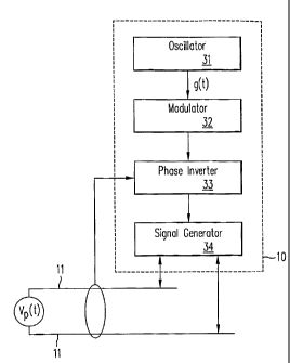
[0023] Figure 2 is a block diagram of a transmitter in
accordance with some embodiments of the present invention.
[0024] Figures 3A through 3D show a schematic diagram of
a switched-resistive load transmitter and conductance
voltage, and current waveforms in accordance with the some
embodiments of the present invention.
- 5d -
CA 02492735 2005-01-14
69790-69
[0025] Figures 4A through 4F show a schematic diagram of
another switched-resistive transmitter and conductance
voltage, and current waveforms in accordance with the some
embodiments of the present invention.
[0026] Figure 5 shows a schematic diagram of a current
source transmitter in accordance with the some embodiments
of the present invention.
[0027] Figures 6A through 6D show current and voltage
waveforms in accordance with the transmitter of Figure 5.
[0028] Figures 7A through 7B show duty-cycle conductance
and current waveforms in accordance with the transmitter of
Figure 3A.
[0029] Figures 8A through 8E show phase-switched
waveforms in accordance with the transmitter of Figure 2.
[0030] Figures 9A through 9C show a schematic diagram of
a DC coupled-inductor transmitter and associated waveforms
in accordance with some embodiments of the present
invention.
[0031] Figures 10A through 10E show a schematic diagram
of an AC coupled-inductor transmitter and associated
waveforms in accordance with some embodiments of the present
invention.
[0032] Figures 11A through 11C show a schematic diagram
of a current-pump resonant-circuit transmitter and
associated waveforms in accordance with some embodiments of
the present invention.
6 -
CA 02492735 2005-01-14
69790-69
[0033] Figures 12A through 12C are block and schematic
diagrams of a transmitter in accordance with some
embodiments of the present invention.
[0034] Figures 13A and 13B are schematic diagrams of a
resonant-circuit transmitter in accordance with some
embodiments of the present invention.
[0035] Figures 14A through 14D are block and schematic
diagrams of receivers in accordance with some embodiments of
the present invention.
[0036] In the present disclosure, like objects that
appear in more than one figure are provided with like
reference numerals.
DETAILED DESCRIPTION
[0037] Figure 1 illustrates how a transmitter 10 and a
receiver 100 are used with a power distribution system. In
some embodiments of the present invention, a transmitter 10
directly connects to a power distribution system through a
wall outlet. In some embodiments, the transmitter 10
directly connects to the distribution wiring by, for
example, jumper wires. The transmitter 10 then energizes a
circuit 11 of the power distribution system. A receiver 100
detects electromagnetic radiation 20 induced by the
transmitter 10. The receiver 100 senses the electromagnetic
radiation 20 emanating from the energized wires of the
circuit.
[0038] With proper modifications, some embodiments of the
present invention may be used to identify circuit elements
or to trace circuits on powered or un-powered lines.
Powered lines may carry either alternating current (AC) or
direct current (DC) at a low or high voltage.
- 7 -
CA 02492735 2005-01-14
69790-69
100391 For un-powered lines, power is disconnected from the circuit breaker
box 12. The
hot and neutral conductors are temporarily connected together to create a
closed circuit
within the local distribution system. For the un-powered cases, the
transmitter 10 requires
an internal power supply. For the powered cases, the transmitter 10 either may
include an
internal power supply, or may tap power directly from the circuit i l
connected to the
power distribution system.
[00401 Some aspects of the present invention are directed towards an improved
transmitter
used to induce a signal along trace wires and.in circuit breakers. Some
aspects of the
present invention are directed towards an improved receiver used to sense a
transmitted
signal emanating from wires and circuit breakers. Some circuits used in a
transmitter
include a dissipative load such as a resistive load or a current source. Some
circuits include
a reactive load such as a coupled inductor or an LC resonant circuit.
[0041] Figure 2 is a block diagram of a transmitter in accordance with some
embodiments
of the present invention. The transmitter 10 includes an oscillator 31, an
optional
modulator 32, an optional phase inverter 33, and a signal generator 34. The
transmitter 10
is electrically connected across one circuit 11 of a power distribution
system.
7a -
CA 02492735 2005-01-14
WO 2004/008159 PCT/US2003/021532
[00421 The oscillator 31 of Figure 2 provides a carrier signal with a
frequency off, to the
modulator. The carrier signal may be any function, for example, a sinusoidal
wave or a
square wave, with a mid-range principal frequency between 120 Hz and 3900 Hz
and may
be set between a pair of adjacent harmonics of potential AC noise generators.
By using a
mid-range frequency f, below 3950 Hz, coupling among circuits is significantly
reduced.
By using a mid-range frequency f, between adjacent pairs adjacent of harmonics
a 50 Hz,
60 Hz or 400 Hz power systems, discrimination and detection by a receiver 100
is
enhanced. Additionally, a transmitter 10 and a receiver 100 pair tuned between
pairs of
adjacent harmonics of multiple power systems may be used on each of these
types of power
systems without retuning or adjustment. For example, a frequency f, of 930 Hz
lies
relatively evenly spaced between pairs of adjacent harmonics of both 50 Hz and
60 Hz
power systems. Of course, many other frequencies that lie between pairs of
adjacent power
line harmonics, such as approximately 570 Hz, 630 Hz, 870 Hz, 1170 Hz, 1230 Hz
and
1470 Hz, are also usable. The frequency f, may be generated in a variety of
ways well
known in the art. Components such as a crystal oscillator or a ceramic
resonator may be
used. Alternatively, the frequency may be synthesized from a powered line
being sensed.
Embodiments using a mid-range carrier frequency between 120 Hz and 3900 Hz and
lying
between a pair of adjacent harmonics may be better understood with reference
to Figures
3A through 6D below.
[00431 The modulator 32 of Figure 2 is also optional. If the modulator is not
implemented,
the carrier provided by the oscillator 31 passes to the phase inverter 33. If
implemented,
the modulator 32 performs additional signal conditioning, such as duty-cycle
modulation.
Duty-cycle modulation periodically allows the oscillator signal to pass. As a
result, duty-
cycle modulation can increase signal-to-noise ratio. The power dissipated by a
transmitter
using duty-cycle modulation can be made the same as a conventional
transmitter,
however, duty-cycle modulation can produce a larger current signal. Duty-cycle
modulation induces a current signal for only a fraction of each transmitted
cycle. The time
for a receiver 100 to acquire and process the signal is increased. Any number
of other
modulation schemes, for example, FSK, MSK, QPSK and spread spectrum, are
possible.
Duty-cycle modulation may be better understood with reference to Figures 7A
and 7B
below.
-8-
CA 02492735 2005-01-14
69790-69
[0044] The phase inverter 33 of Figure 2 is incorporated into some embodiments
of the
present invention. The phase inverter 33 may be operated before or after the
modulator 32.
The phase inverter 33 performs phase inverting or phase switching. The
instantaneous
polarity of the line may be sensed and a phase inverse signal imposed on the
transmitted
signal. The phase switching process may be implemented using combinational
logic or an
algorithm in a microcontroller or microprocessor. Phase switching prevents a
carrier from
being modulated as a function of the line frequency and confers two benefits:
first, more of
the current goes into the target frequency rather than being divided into side-
bands; and
second, the primary signal frequency received is not a function of line
frequencies (e.g. 50,
60, or 400 Hz). Phase switching increases the first harmonics of the
transmitted signal,
thus increasing the probability of detection by the receiver 100 Phase
inverting or phase
switching may be better understood with reference to Figures 8A through 8E
below.
[0045) The signal generator 34 of Figure 2 may be either a dissipative load or
a reactive
load such as a switched-resistive load (as shown in Figures 3A and 4A), a
switch-current
source (as shown in Figure 5), a switched coupled inductor (as shown in
Figures 9A and
1 OA), or an LC resonant circuit (as shown in Figure 11A). The signal
generator 34 of
Figure 2 may be better understood with reference to the description below.
[0046] In the following equations, the relative phase between the switched
load g(t) and
the line voltage vp(t) is ignored for mathematical convenience. The results
focus on the
relative magnitudes of various frequency components.
[0047] Figures 3A, 4A and 5A are schematic diagrams of transmitters in
accordance with
some embodiments of the present invention.. Figure 3A shows a simple
transmitter
including a switched-resistive load transmitter with conductance G.
Conductance G is
applied to the circuit by a switch SI switching ON and OFF at a carrier
frequency off,
having a period of To=1/f . The carrier frequency f, controls switch S1 such
that the
conductance G appears as represented in Figure 3B. When the switch is not
conducting
(OFF), the conductance is zero. When the switch is conducting (ON), the
conductance is
=
G. A resistive load with conductance of G = (11R) [mhos] is switched at
frequency f,
co ,127r. The resulting switched conductance signal g(t) = G * square(coc)
appears as a
-9-
CA 02492735 2005-01-14
69790-69
square wave with a conductance of G for the first-half of the duty-cycle and
zero mhos for
the second-half of the duty-cycle.
10048] Multiple factors are considered when selecting the value of the carrier
frequency f.
Carrier frequency f, selected may be selected such that the value lies between
a pair of
adjacent harmonics of various power systems. By selecting a frequency f,
between a pair
of adjacent harmonics of a power system, the sensitivity requirements for a
receiver's
detection circuitry are lessened. By selecting a frequency f, that lies
between the various
pairs of adjacent harmonics of different power systems, the
transmitter/receiver pair may be
used in various geographic locations using different power line frequencies.
[0049] Common power systems in the United States use a 60 Hz line frequency.
Harmonics of these systems lie at multiples of 60 Hz (e.g., 120 Hz, 180 Hz,
240 Hz and 300
Hz). Candidate carrier frequencies that lie between a pair of adjacent
harmonics of a U.S.
system are approximately 90 Hz, 150 Hz, 210 Hz, 270 Hz and so on. Common power
systems in Europe use a 50 Hz line frequency. Harmonics of these systems lie
at multiples
of 50 Hz (e.g., 100 Hz, 150 Hz, 200 Hz, 250 Hz and 300 Hz). Candidate carrier
frequencies
that lie between a pair of adjacent harmonics of a European system are
approximately 75
Hz, 125 Hz, 175 Hz, 225 Hz and so on. Candidate carrier frequencies that lie
between a
pair of adjacent harmonics of both 50 Hz and 60 Hz include approximately 80
Hz, 165 Hz,
220 Hz, 270 Hz, 330 Hz, 380 Hz and so on.
[0050] Carrier frequency f, selected may also be selected such that .the value
is a mid-range
between frequency, that is, a frequency 120 Hz and 3900 Hz. The power spectrum
from
DC to 120 Hz of a typical power system often includes excessive noise. As the
carrier
frequency is increased, a transmitted signal more easily couples to
neighboring circuits.
Coupling to neighboring circuits is undesirable but some coupling capability
is necessary
because a transmitted signal must at least couple to a receiver's antenna in
order for the
receiver to sense the transmitted signal. As the carrier frequency increases,
the likelihood
that a transmitted signal will be detected also increases, however, at the
cost of stronger
coupling to neighboring circuits. Above approximately 4000 Hz, inexpensive
receivers can
be built to receive the coupling transmitted signal. Below approximately 3900
Hz, the
-10-
CA 02492735 2005-01-14
69790-69
typical transmitters and receivers are less efficient and are not sensitive
enough to detect
the transmitted signal.
[00511 The more efficient transmitter/receiver pair of the present invention
balances the
need for coupling by way of improved transmission and reception techniques.
Preferably, a
selected carrier frequency f, lies between approximately 240 Hz and 2000 Hz
and lies
relatively evenly spaced between adjacent harmonics of each 50 Hz, 60 Hz and
400 Hz
power systems.
[00521 Figure 3C shows the voltage vp(t) supplied by an AC power network
having a
period of Tp=1/fp. Ignoring the relative phases, the AC voltage signal vp(t) =
Vp cos(wp t) is
a sinusoidal wave at frequency fp = wp/2rc. In a typical 50 Hz power network,
voltage vp(t)
has peaks at Vp equal to approximately 160 volts (110 volts RMS) (e.g.,
Japan) or
325 volts (220 volts RMS) (e.g., Europe). The period Tp of a 50 Hz signal is
approximately 20 milliseconds (msec). In a typical 60 Hz power network,
voltage vp(t) has
peaks at Vp equal to approximately to 160 volts. The period Tp of a 60 Hz
signal is
approximately 167 msec.
[0053] Current ip(t) through the resistive load creates a voltage drop of
approximately Vp
across the resistive load G. Applying Ohm's law, a current through the
resistive load
appears as a pulsed current ip(t) that follows the envelope of vp(t) and is
scaled by the
product of voltage vp(t) and switched conductance G through the switch as
shown in Figure
4D. The current ip(t) is induced on the pair of conductors making up the
circuit 11 to be
tested. The cumulative resistance in the circuit I 1 and of the non-ideal
components of the
transmitter 10 is represented by resistor R. The cumulative resistance R,
though not shown
in subsequent schematic diagrams, is assumed to be present. The induced
current ip(t)
creates electromagnetic radiation 20 that a receiver 100 is designed to sense.
Here, the
analysis was shown for the AC power case. A similar analysis may also be
applied if the
voltage source vp(t) represents a DC power case or an un-powered closed
circuit.
[0054] Figure 4A shows an alternative embodiment to the simple transmitter of
Figure 3A.
The circuit includes a switched-resistive load with conductance G that induces
a current
i2(t) on to the line through a full-wave bridge rectifier having four diodes
D. One advantage
of using a rectifier is that the bi-directional switch may be replaced with a
unipolar switch
-11-
CA 02492735 2005-01-14
WO 2004/008159 PCT/US2003/021532
SI that can be implemented with a single FET, a single power MOSFET or a
single bipolar
transistor.
[0055] Figure 4B shows the transmitter's conductance g(t) as the switch opens
and closes.
Figure 4C shows the voltage vp(t) supplied by the power system. Figure 4D
shows the
rectified voltage v2(t) after the full-wave rectifier and before the switched
conductor.
Figure 4E shows the current i2(t) through the switch SI. Following Ohm's law,
current i2(t)
is the product between the switched conductance g(t) and the rectified voltage
v2(t).
Current i2(t) passes through the rectifier producing current ip(t), which
induces
electromagnetic waves 20 that emanate from circuit 11.
[0056] Figure 4F shows the induced current ip(t) for a switched-resistive load
transmitter
applied to an AC power system. The current appears as a pulse train scaled by
the
envelope of the AC power and by the conductance G of the resistive load.
[0057] Figure 5 shows an alternative embodiment to the transmitter of Figure
4A. The
resistor with conductance G in Figure 4A is replaced with a current source 12.
A switch S1
placed in series with the current source 12 defines a switched-current source.
A switched-
current source may be implemented with an emitter-follower style amplifier.
The
schematic diagram of Figure 5 is further described with reference to the
timing diagrams of
Figures 6-8 described below.
[0058] Figure 6A shows the current i2(t) switching on and off at the carrier
frequency f,.
Figures 6B and 6C show the voltages before and after the rectifier as
described above.
[0059] Figure 6D shows the current ip(t) that is induced on circuit 11 by the
transmitter 10.
The current signal i2(t) generated by the current source and switch passes
through the
rectifier and appears as a pulse train with each pulse having a constant
magnitude but a sign
equaling the sign of the AC power system's voltage vp(t). Unlike cases using a
resistive
load, the amplitude of current ip(t) using a current source is a function of
the sign and not of
the amplitude of vp(t).
[0060] According to some embodiments, for each of the circuits shown, the
carrier
frequency may be set at a mid-range and the carrier frequency selected may be
centered
-12-
CA 02492735 2005-01-14
69790-69
between a pair of adjacent harmonics. Additionally, duty-cycle modulation and
phase-
switching, shown below, may be used.
100611 Figures 7A through 7B show duty-cycle conductance and current waveforms
in
accordance with the schematic diagram of Figure 3A. Every T2 seconds, the
modulator 32
of Figure 2 switches on (enables) the conductance g(t) pulse train for a
period of TON
seconds, as shown in Figure 7A. After TON seconds, the modulator 32 halts
(disables) the
pulse train for a period of TOFF seconds. The ration of TON to TOFF ranges
from 1':1 to 1:10.
A ration of TON. TOFF = 1:1 represents a 50% ON duty-cycle and allows a
receiver to reduce
the amount of time it needs to provide an update. A ration of TON: TOFF =1:10
represents
approximately a 10% ON duty-cycle and reduces power dissipation in a
transmitter and
allows the transmitter to place a greater amount of power in the transmitted
burst of pulses.
The sum of TON and TOFF defines T2. The period T2 is also limited by estimated
patience of
an operator, that is, by the amount of time that an operator will be expected
to wait between
updates. Additionally, the-ratio between TON and To ranges from 50:1 to 500:1,
thus
allowing 50 to 500 pulse of length To in each ON period TON.
[00621 For example, with a carrier frequency f~ = 930 Hz, To equals
approximately 1 cosec,
ToN ranges approximately from 50 msec to 500 msec, and TOFF ranges
approximately from
50 msec to 1 second. In some embodiments, the carrier frequency f, = 930 Hz,
TON equals
approximately 250 msec and TOFF equals approximately 750 msec, thus resulting
in a 25%
duty-cycle.
[00631 Figure 7B shows the resulting current ip(t) induced on circuit 11. If
using switched
conductance, the current ip(t) will follow the envelope of the voltage vp(t)
but scaled by the
conductance G as shown. When the conductance g(t) is zero between groups of
pulses, the
current ip(t) will also be zero. The implementation of duty-cycle modulation
to the
schematic of Figure 3A is exemplary only and is not meant to limit other
implementations.
If the conductance G of Figure 3A is replaced with the current source of
Figure 5, a similar
current ip(t) results; however, the sinusoidal envelope is removed leaving a
constant
envelope.
[00641 Figures 8A through 8E show phased-switched conductance and current
waveforms
in accordance with the schematic diagram of Figure 3A. Figure SA shows the
voltage vp(t)
-13-
CA 02492735 2005-01-14
69790-69
supplied by the power system. Figure 8B shows m~ (t), which represents the
sign of vp(t).
Figure 8C shows the transmitter's conductance g(t) before phase-switching.
Figure 8D
shows the transmitter's conductance g4 (t) after phase-switching. The
transmitter's
conductance g4 (t) is produced by the product of m4(t) and g(t). Figure 8E
shows the
current ip(t) induced on circuit 11. The current i2(t) is the product between
the switched
conductance g4 (t) and the voltage vp(t). Current i2(t) passes through the
rectifier producing
current ip(t), which induces electromagnetic waves 20 in the circuit 11. If
the current
source of Figure 5 replaces the conductor, the currents i2(t) and ip(t) do not
follow the
envelope of v(t).
[0065] Without phased-switching, a classical modulator modulates a signal x(t)
with a
sinusoidal carrier signal s(t) at frequency f = co, / 2,r. If the signal x(t)
is also a sinusoidal
wave but at frequencyf = wx / 2a, where f,, <f, / 2, the resulting frequency
domain
components of x(t) * s(t) have equal magnitude lying at frequencies (f,J) and -
{f ). If
x(t) represents vp(t), then, to first order, the square wave signal switched
load g(t) at
frequencyf equals the sinusoidal signal s(t) at frequencyf, when frequency f, -
h.
Therefore, without phased-switching, the classical modulation produces
frequency domain
components at frequencies (f p) and -(f4).
[00661 Typical distribution systems operate at a line at frequencyf of 50 Hz,
60 Hz or 400
Hz. With a domestic or industrial power system in the U.S., the line provides
a signal with
frequency with fp = 60 Hz. A load frequency off = 870 Hz results in signals at
(f tf) of
810 Hz and 930 Hz. The energy in the resulting signal is equally split and the
transmitted
frequencies are dependent on the line frequencyf of the power system.
[0067] A Fourier series expansion of the conductance g(t)-shown in Figure 3B
is
g(t)=a0 + an x sin((2n --1)W 8 t)
n=1
where
-14-
CA 02492735 2005-01-14
WO 2004/008159 PCT/US2003/021532
G
ao =_
2
2G
an =
it (2n -1)
[0068] The current ip(t) induced on the line is:
ip(t) - VP(t) = g(t)
_ (VP COS(co pt))= (ao +' an = sin((2n -1)C)gt)
n=1
=V - a =cos cot + a V 'COS(' i t =sin 2n-1 t
P 0 ( p) n p p) (( / g )
n=1
with
sin A cos B = sin(A + B) + I sin(A - B)
then
ip(t) = VP = a0 = cos(COpt)
+ an = V p = {sin((2n - l)W)gt + ao pt)- sin((2n - l)cogt - w pt)}
n=1 2
[0069] The magnitude of the first harmonic is (aõVp/2) which equals (GVp/ir).
To reduce
the impact of the line frequency, the switching of the load can be modified by
using phase
inversion to shift the energy from frequencies at (f f,,) to a frequency
off,.
[0070] By replacing conductance g(t) with phase-switched conductance ge(t),
the current
ip(t) induced on the line becomes:
go (t) = m~ (t) = g(t)
and
-15-
CA 02492735 2005-01-14
WO 2004/008159 PCT/US2003/021532
ip(t) _ VP(t) - go (t)
_ (VP = cos(w pt)) = (MO (t) = ao + Z an = sin((2n -1)cogt)
n=1
I
=VP - m, (t) - a0 =cos(wpt) +mo (t) = I an - VP =cos(cot) =sin(( 2n-I~ t)
pg /
n=1
with
MO (t) cos(w pt) = Icos(c) Pt)I
then
ip(t) = V= a o w t I+ Icos w t I a V. sin((2n - I)w gt)
VP 0 ( P) ( P) =Zn P
n=1
with
Vp = Icos(w pt)= bo + bn = cos((2n - I)co gt)
n=1
then
ip(t) = a0 = VP . 1cos(w pt)I
+ bo + bn = cos((2n -1)wgt) an = sin((2n -1)wgt)
n=1 n=1
Z
=
a- v p t+ an b= sin 2n -1)cot
0 p I (w p)I ~ rr 0 (( g )
n=1
+ Z bn = cos((2n -1)wgt) a,,, = sin((2m -1)wgt)
n=1 m=1
= ao = VP = Icos(w pt)I + E an = b0 = sin((2n -1)wgt)
n=1
oo co
+IZan,bn =sin((2m-1)wgt)=cos((2n-1)cogt)=
n=1 m=1
[0071] Therefore, the amplitude of the spectral component of ip(t) at wg is
(albo), which
equals (2VpI7t)*(2Vplzc) = (4VPGIic2). That is, when using phase switching the
magnitude of
the first harmonic is (4GV /rc2). The ratio of the non-phase-switched first
harmonic.
-16-
CA 02492735 2005-01-14
WO 2004/008159 PCT/US2003/021532
magnitude (a,Vpl2) and phase-switched first harmonic magnitude (4GVPlIr 2)
shows that
phase-switching provides a 27% improvement in amplitude over an equivalent non-
phase-
switched implementation.
[0072] Similarly, for the current source circuit of Figure 5, the amplitude of
the first
harmonics can be shown to be (2Iolir) without phase shifting and (41,/n2) with
phase
shifting, thus providing a theoretical improvement of approximately 57 %.
[0073] Features described above, namely: (1) use of a carrier frequency set at
a mid-range;
(2) use of a carrier frequency centered between a pair of adjacent harmonics;
(3) use of
duty-cycle modulation; (4) use of phase-switching; may be applied in
conjunction with a
dissipative load (e.g., a resistive load or a current source, described above)
or with a
reactive load (e.g., coupled inductors and LC resonant circuits, described
below). These
features may also be combined with one another. For example, a mid-range
carrier
frequency centered between a pair of adjacent harmonics may use a circuit
including a
dissipative load or a reactive load.
[0074] The techniques described above may be replaced or supplemented with the
two
reactive techniques described below. The first reactive technique uses the
magnetic field of
mutually coupled inductors to store and discharge energy and is shown for both
the DC and
AC cases. The second reactive technique uses a series resonant circuit.
[0075] Figure 9A is a schematic diagram of a DC coupled-inductor transmitter
in
accordance with some embodiments of the present invention. The voltage source
vp(t) is
assumed to be a DC voltage source. Two magnetically coupled inductors L1 and
L2 are
coupled with reverse polarities. A first chain includes an inductor LI and a
switch SI
connected in series. A second chain includes an inductor L2 and a diode D2
connected in
series. The two chains are connected in parallel with the DC power source
having voltage
vP(t).
[0076] Figures 9B and 9C show switch position and current waveforms in
accordance with
the schematic diagram of Figure 9A. Figure 9B shows the position of switch Si
relative to
Figure 9C. The waveforms assume switch SI is open (turned OFF) at time t < 0,
there is
ideal coupling between L1 and L2, and there is equality of the self-
inductance. When Si is
-17-
CA 02492735 2005-01-14
WO 2004/008159 PCT/US2003/021532
closed (turned ON), a current ip(t) = II begins to flow with the indicated
polarity. When SI
is subsequently opened (turned OFF), the collapsing magnetic field causes a
current i(t) = -
12 to flow. From an energy perspective, energy accumulates in the magnetic
field during
the period when the switch S1 is closed (turned ON) and released when the
switch S1 is
opened (turned OFF). A receiver 100 may be used to detect electromagnetic
radiation
emanating from the circuit 11 as a result of the saw tooth current ip(t). This
coupled-
inductor technique shown for a DC case may be extended to an AC case source as
show in
Figure 10A.
[0077] Figure 1OA is a schematic diagram of an AC coupled-inductor transmitter
in
accordance with some embodiments of the present invention. The voltage source
vp(t) is
assumed to be an AC voltage source. Two magnetically coupled inductors LI and
L2 are
coupled with reverse polarities as with the DC case. A first chain includes an
inductor L1,
a switch S1 and a diode DI connected in series. A second chain includes an
inductor L2, a
switch S2 and a diode D2 connected in series. The two chains are connected in
parallel
with the AC power source having voltage vp(t).
[0078] Figures l OB through 10E show switch position and current waveforms in
accordance with the schematic diagram of Figure I OA. Figure I OB shows the
voltage vp(t)
supplied by an AC power network having a period of Tp=1/fp. Again, the
switching
frequency (carrier frequency fi) is assumed to be substantially greater than
the frequency of
the power signal. Figures 10C and l OD show the switching of switch Si and S2.
While
the polarity of vp(t) is positive, switch S2 is held in the connected position
and switch S1 is
actively modulating the current by turning ON and OFF at the selected carrier
frequency.
While the polarity of vp(t) is positive, the circuit operates substantially as
described with the
DC case above. When the polarity of vp(t) changes from positive to negative,
switch S1 is
held in the connected position and switch S2 begins actively modulating the
current by
turning ON and OFF at the selected carrier frequency. While the polarity of
vp(t) is
negative, the circuit operates equivalent via symmetry. Figure I OE shows the
resulting
current signal ip(t) induced on the circuit 11.
[0079] Figure 11 A is a schematic diagram of a resonant-circuit transmitter in
accordance
with some embodiments of the present invention. In accordance with other
embodiments
-18-
CA 02492735 2005-01-14
69790-69
of the present invention, a reactive system uses a series-resonant circuit to
share energy
storage between magnetic and electrical fields. An inductor L is connected is
series to a
capacitor C. A current-source 12 is connected in series with a switch Si. The
current-
source 12 and switch S 1 are connected in parallel across the capacitor C. The
power system
provides an AC voltage vp(t) and the circuit induced a current ip(t) on to the
circuit 11. The
current source 12 and switch S I define a switched current source.
100801 The carrier frequency f is selected as described above. The inductor L
and
capacitor C of the LC resonant circuit are selected to resonate at the carrier
frequency f,.
The switched current source is switched ON and OFF at the rate of the carrier
frequency f,
and is used to inject a small amount of current into the LC circuit.
[0081] Figure 1 I B shows the switch S I ON and OFF transitions. The duty-
cycle of the
switch S 1 is selected such that the injected current compensates for the
natural and parasitic
resistive elements of the transmitter 10 and circuit 11. If the switch is
opened and closed at
the resonant frequency f, of the series LC circuit, the energy lost is
replenished. By
adjusting the duty-cycle of the switch and the magnitude of the current
source, a current
ip(t) can be maintained at very nearly sinusoidal wave with frequency f . In
some
embodiments the duty-cycle is approximately 3% ON.
[0082] Figure 11C shows the current waveform in accordance with the schematic
diagram
of Figure 11A. Generally, the LC circuit resonates at the carrier frequency f.
In the ideal
case, that is, without resistive losses, the LC circuit would continue to
resonate once
started. Assuming the ideal case for the LC circuit, the current ip(t) = A
sin(o),t), where f =
2'ao, is the resonant frequency of the LC circuit and A is a scalar constant.
The current ip(t)
in will remain A sin (coat) for all time and there is no energy dissipated.
[0083] For the realistic case, wiring resistance, component imperfections,
parasitic
resistances in the capacitor and inductor cause small amounts of power to
dissipate from
the LC circuit. If left unattended, the current envelope would slowly
attenuate until no
current was resonating in the LC circuit. If power is periodically injected
into the circuit
with the switched current source, the decaying current is replenished, thus
maintaining a
relatively constant current envelope.
-19-
CA 02492735 2005-01-14
69790-69
[00841 The circuit shown in Figure 11 works equally well with either DC or AC
power
sources. If the AC source frequency is much less than the resonant frequency.
The only
change is an addition to i of a current at the AC source frequency. The fact
that the signal
current is not dependent on the value of the source voltage is beneficial for
designs that are
used over a range of voltages.
100851 The advantage of the series resonant circuit vis-a-vis the coupled
inductor circuit is
that it is much cheaper. The disadvantage is the limited opportunities for
modulation - it
functions best at a single frequency whereas the coupled inductor circuit can
be modulated
easily. Both share the same concept: alternate between energy-accumulation and
energy-
sourcing to generate a current signal.
100861 Figures 12A, 12B and 12C are block and schematic diagrams of a
transmitter.
The transmitter 10 of Figure 12A includes a front-end filter
41, a phase extractor 42, a microcontroller 43, a rectifier 44 and a switched
load 45. The
front-end filter 41 filters high bandwidth noise. The phase extractor 42
tracks the
frequency and phase of the incoming AC voltage vp(t). The extracted frequency
and phase
information is passed to the microcontroller 43. The microcontroller 32
provides a signal
to the switched load 45 to control the switching of the load's switch. If
phase-switching is-
implemented, the microcontroller 43 can use the power frequency and phase
information to
switch the phase of the switch control signal sent to the switched load 45.
The rectifier 44
provides a bi-polar current source that is switched ON and OFF by the
microcontroller 43.
[00871 Figures 12B and .12C show a detailed implementation of the current
source
transmitter of Figure 5. A clip-clamp circuit which serves as phase extractor
42 taps the
input AC voltage vp(t) and provides a square wave with a high of +Vpp volts, a
low of 0
volts and a frequency of fp to the microcontroller 43. The microcontroller 43
is
programmed to provide a switching signal that transitions at the carrier
frequency f,7. If
phase-switching is enabled, the microcontroller 43 adjusts the switching
signal before
sending it to the switch. The switching signal passes through resistor R12 to
the switch.
The current source 12 and switch Si of Figure 5 are replaced with the emitter-
follower
circuit shown. The switch, here implemented with transistor Q4, is controlled
through the
base of Q4 by the microcontroller's switching signal. When the transistor Q4
is turned ON,
-20-
CA 02492735 2005-01-14
WO 2004/008159 PCT/US2003/021532
current is drawn from the full-wave bridge rectifier 44 having for diodes D3
D4 D5 and
D6. The current drawn appears as ip(t) going into the transmitter 10.
Additionally, the
LED D 11 provides a visual indication to the electrician that the line is hot.
[00881 Figure 12C is a further detailed version of Figure 12B, and shows a
voltage
generator and a PIC processor. A shunt-voltage generator, comprised of diodes
D1 and D2,
resistor RI and capacitor Cl, may be used as a reference for the clip-clamp
circuit 42 and
can be used to power the microcontroller 43. Also shown is a PIC12C508
microcontroller
43. The PIC12C508 processor is an 8-pin, 8-bit CMOS microcontroller
manufactured by
Microchip Technology Inc. (2355 W. Chandler Blvd., Chandler, AZ 85224). The
processor synthesizes the carrier frequency switching signal, for example, at
930 Hz.
[0089] Figures 13A and 13B are schematic diagrams of a resonant-circuit
transmitter in
accordance with some embodiments of the present invention. The low pass filter
of Figure
13B has been replaced with a series RLC circuit 50. The RCL circuit is
designed to
resonant at the resonant frequency f. The switched current source 45 injects
current
through the rectifier 44 into the RCL resonant circuit 50 to compensate energy
dissipated in
the circuit. A resistor R11 may be used to keep a constant current flowing
through the
circuit while the transistor Q4 is OFF.
[0090] In some embodiments, the microcontroller 43 synthesizes a 930 Hz
carrier
switching signal from vp(t). The emitter-follower is switched at a rate of
930Hz with an on-
time about 3 % of the period.
[00911 Figure 13A, 13B transmitter operates over a wide range of voltages. The
lowest
operating voltage is defined by both the diode drops and by the low end of the
emitter-
follower amplifier's operating range. The high operating voltage is defined by
the
maximum voltage rating of the components. The components in Figure 13B are
designed
for an AC voltage range of 100 to 277 V,,,,s at 50 or 60 Hz.
[00921 The transmitters described above induce a current ip(t) on the circuit
11. A receiver
100 is required to sense the electromagnetic radiation resulting from the
induced current
ip(t). The receiver typically needs no physical contact with the circuit 11.
The signal is
measured by sensing the electromagnetic field 20 in circuit I 1 with an
unshielded inductor,
-21 -
CA 02492735 2005-01-14
69790-69
hall-effect device, or flux gate. Passive- and/or active-analog signal-
conditioning circuits
with a band-pass transfer function centered at the signal carrier frequency f~
precede a
signal isolator that produces a metric indicative of signal intensity.
[0093] In some embodiments, a two-step process generates the signal intensity
metric.
First, a raw metric is derived through for example very-narrow band-pass
filtering, or
asynchronous demodulating of the input. Second, the raw metric is refined
through
integration for a period of time equal to an integral number of line frequency
cycles to yield
zero responses of line frequency harmonics. The integrator may be implemented,
for
example, with an analog gated-integrator or with digital arithmetic. Previous
approaches to
isolate the desired carrier frequency used simple linear time-invariant
filtering rather than
the time-variant technique disclosed here. These previous approaches do not
provide the
high degree of immunity to interference as the present invention.
[0094] Additionally, a receiver 100 may include automatic calibration. In some
embodiments, automatic calibration is performed by using a combination of
memory and
comparators. The memory holds the value of the largest measurement seen as the
electrician initially scans the candidates. Subsequently, the indicator(s)
will show a
positive result at the target. The comparator discriminates against the
maximum and sub-
maximum readings. The memory may be implemented, for example, digitally with
conventional on-board or separate memory, or via analog circuitry such as a
sample-and-
hold circuit. Similarly, the comparator may be implemented with an analog
comparator or
with a digital arithmetic processor.
[0095] Figures 14A through 14D are block and schematic diagrams of receivers
in
accordance with some embodiments of the present invention. A fluctuating
magnetic field
generated by the signal current produces a potential across the sensor 101 or
transducer
201. The potential is conditioned then band-pass filtered with filter 102 or
band pass filter
202. A microcontroller 103, for example a PIC12C671, includes an ADC, which
converts
filtered result s(t) into a digital word. The magnitude of the magnetic field
intensity s(t) at
_
carrier frequency f, may be used as the raw metric. For example, at a carrier
frequency f,
930 Hz, the raw metric may be computed as:
-22-
CA 02492735 2005-01-14
WO 2004/008159 PCT/US2003/021532
raw_ metric = I s(t)I = (s(t) sin(27c(930)t))2 + (s(t) cos(2 (930)t))2
[0096] The raw metric may be integrated for a set period of time, for example,
0.1
seconds, thus produce a refined metric that is zero at all frequencies that
are multiples of 10
Hz except 930 Hz. Averaging the results from two integration operations then
forms a final
measurement 5 times a second.
[0097] Each time a new measurement is performed it is compared to a reference.
If the
measurement is less than a set percentage of the reference, then, if used, a
red LED or other
proper optical indicator illuminates. If the measurement is greater than the
set percentage
of the reference, a green LED or other proper optical indicator illuminates
and/or a buzzer
or other audio indicator sounds. The set percentage may be for example between
approximately 70 to 95%, such as 90%. Additionally, if the measurement is
greater than
the reference, then the reference is set to one-half of the sum of the current
reference and
the last measurement. Alternatively, if the measurement is greater than the
reference for
two consecutive measurements, then the reference is set to one-half of the sum
of the
current reference and the last measurement. The process repeats, thus updating
the
reference value and providing visual/audio indications on an ongoing basis as
appropriate.
The process described implements automatic calibration in the receiver.
[0098] A method for finding an electrical circuit using a transmitter and
receiver as
described above includes connecting the transmitter to an electrical circuit,
inducing a
modulated signal at a carrier frequency onto the electrical circuit, sensing
the electrical
circuit with a receiver which detects the carrier frequency, by generating a
metric, saving
the metric as a reference, generating a next metric, comparing the reference
to the next
metric, and if the next metric is a set percentage of the reference,
generating an alert
indication to an operator, comparing the reference to the next metric; and if
the next metric
is greater than the reference, setting the reference to the average of the
next metric and the
reference; and repeating the acts of generating the next metric, comparing and
generating
the alert, and comparing and setting the reference.
[0099] Another method for fording an electrical circuit using a transmitter
and receiver as
described above includes providing a carrier frequency between approximately
120 Hz and
-23 -
CA 02492735 2005-01-14
WO 2004/008159 PCT/US2003/021532
approximately 3900 Hz, modulating the carrier frequency, generating a signal
across a
modulator and a load, coupling the signal to the electrical circuit; and
detecting the signal
in the conductive circuit.
[00100] For identifying circuit elements such as junctions, breakers, and
fuses in powered
AC distribution systems all of the techniques apply and the transmitter uses
the available
power to generate the signal by loading the line. The same methods may be used
on a
powered DC system (DC power systems are often used in places such as aircraft,
ships,
locomotives and associated rolling freight, road vehicles and spacecraft) but
then only
numbers 1 and 4 above confer any benefit.
[00101] For tracing a circuit in a powered AC system the automatic calibration
is deleted
from the receiver or simply disabled in a receiver that can perform both
identification and
tracing. Then the signal level is measured against an unchanging reference
(supplied by a
factory setting, manual calibration, or automatic calibration). Tracing is
performed via a
"closer/further" indication to the electrician by visual and/or audio means.
In this
application all of the techniques listed are applicable except number 4. When
tracing
powered DC systems the same modifications apply and all of the techniques may
be used
but only number 1 confers any benefit.
[00102] Both identification and tracing as described in the previous two
paragraphs can be
extended to un-powered systems through the simple expedient of providing the
transmitter
with an appropriate power source in series with the signal generator of figure
2 and
shorting the main service (see Figure 1) of the distribution system in
question.
[00103] The above detailed descriptions are provided to illustrate specific
embodiments of
the present invention and are not intended to be limiting. Numerous
modifications and
variations within the scope of the present invention are possible. The present
invention is
defined by the appended claims.
-24-