Note: Descriptions are shown in the official language in which they were submitted.
CA 02493130 2005-O1-20
WO 2004/011848 PCT/US2003/023504
METHOD AND APPARATUS FOR USING
LIGHT EMITTING DIODES FOR CURING
CROSS-REFERENCE TO RELATED APPLICATIONS:
This application claims benefit of priority of U.S. Provisional Application
Nos.
60/398,635, filed July 25, 2002; 60/405,432, filed August 23, 2002;
60/410,720, filed
September 13, 2002; 60/418,948, filed October 8, 2002; 60/420,479, filed
October 22, 2002;
60/467,702, filed May 3, 2003 and 60/476,004, filed on June 4, 2003.
FIELD OF THE INVENTION:
This invention relates to the field of light emitting diode ("LED")
technology,
particularly to improvement in the output of light therefrom for curing
curable compositions
and forming cured parts from curable composition after exposure thereto.
BACKGROUND OF THE INVENTION:
Heat can damage sensitive electronic components, degrading reliability and
hampering the ability to concentrate higher power levels into smaller
packages. Many
applications would benefit from the ability to closely package LEDs into
compact
configurations, but the heat levels generated have always been a limiting
factor. As LEDs
become more sophisticated, eliminating internal heat build-up has also become
increasingly
difficult. Devices are becoming more powerful and creating solutions for
removing the
resulting heat generation often pose great challenges.
U.S. Patent Publication No. 2003/0036031 to Lieb et al. discloses a light-
emitting
handpiece for curing light-curable dental resins and similar materials. The
device includes a
CA 02493130 2005-O1-20
WO 2004/011848 PCT/US2003/023504
head portion for supporting a LED light source, a tubular handle portion for
containing a
power source for energizing the LED light source and a neck portion that
interconnects the
head and handle portions. The head and the neck portions are integrally formed
from a
common, thermally conductive material and operate to provide a heat sink for
the LED. A
substantial portion of the light source housing itself functions to dissipate
sufficient thermal
energy away from the LED allowing the LED to be operated for a time interval
sufficient to
effect resin curing.
In U.S. Patent Publication No. 2003/0021310 to Herding, there is disclosed a
method
and apparatus for cooling electronic or opto-electronic devices. The apparatus
includes the
device mounted on a heat sink assembly within a can having a can body and a
can header
thermally coupled to the heat sink assembly and closing the can body and a
thermal
conductor outside the can and having a first portion attached to at least part
of an edge of the
can header and a second portion attached to a thermal sink outside the can.
In U.S. Patent No. 6,159,005 to Herold et al., there is disclosed a small,
light-weight
handy device for photo polymerizing synthetic materials. The device includes a
built-in
battery, a light source constituted by an LED which emits a small useful
spectrally range
only, thereby avoiding any heat radiation. The LED is preferably located at
the tip of the .
device directing towards the site to be polymerized.
In U.S. Patent No. 6,523,959 to Lu et al., there is disclosed a cooling device
utilized
to cool a liquid crystal panel and polarizer of an optical system in a liquid
crystal projector.
The cooling device includes a heat dissipation system comprising a plurality
of heat pipes
disposed at the two flank sides of said liquid crystal panel.
CA 02493130 2005-O1-20
WO 2004/011848 PCT/US2003/023504
None of these U.S. patent documents disclose LED cooling in a manner to
dissipate
internal heat energy and packaging the same to achieve maximum light output.
Thus, a need
exists for cooling the LEDs and mounting the same on the heat pipes in a
manner which
greatly surpasses the performance of conventional cooling techniques and
benefit high-
density, miniatured LED components. Furthermore, there is a need for a novel
LED
packaging technology that channels heat away via state-of-the-art micro heat
pipes that
perform far more efficiently, and in much more compact space, than
conventional heat sink
technology.
SUMMARY OF THE INVENTION:
In a first embodiment of the present invention there is provided a method and
device
for curing adhesives on a surface. The method includes providing at least one
LED, passing a
coolant into the LED through at least one channel to effect cooling of the LED
and irradiating
the adhesive on the surface with the LED to cure the adhesive. The device
includes a power
supply, a radiation source having a radiation output and including at least
one LED coupled
to the power supply and at least one channel coupled to the LED, wherein a
coolant is passed
into the LED via the channel thereby cooling the LEDs to deliver a high light
output on the
adhesives.
In a second embodiment of the present invention there is provided a method for
cooling LEDs. The method includes providing at least one LED, connecting at
least one
channel to the LED to create a path and injecting a coolant through the
channel to cool the
LEDs.
CA 02493130 2005-O1-20
WO 2004/011848 PCT/US2003/023504
In a third embodiment of the present invention, there is provided an LED
curing
device. The device includes a tubular body having two opposing ends, an LED
body
including a highly conductive surface placed at one opposing end and a heat
pipe connected
to the conductive surface of the LED body. The heat pipe serves to transport
heat away from
the LED body.
In a fourth embodiment of the present invention, there is provided a device
for
transporting thermal energy. The device includes a copper heat sink, an array
of LEDs and at
least one heat pipe of tubular shape. The copper heat sink has at least one
vapor cavity. The
array of LEDs are attached to the heat sink wherein a long axis of the vapor
cavity is
substantially perpendicular to the p-n junctions of the LEDs. The heat pipe of
tubular shape
is inserted into the heat sink via the vapor cavity, wherein thermal energy is
transported away
from the array of LEDs in a substantially opposite direction from light
emitting from the
LED.
In a fifth embodiment of the present invention, there is provided an LED
device
package. The LED device package includes a conductive substrate, a heat pipe
connected to
the conductive substrate and at least one LED mounted onto a tip of the heat
pipe, wherein
heat is transported away from the LED.
In a sixth embodiment of the present invention, there is provided an LED
curing
device. The LED curing device includes a tubular body, an LED body, a heat
pipe, a power
source, a fan and a heat sink/exchanger. The tubular body has two opposed ends
including a
wide end and a tip end. The LED body includes a conductive surface and is
placed at the tip
end of the tubular body. The heat pipe extends through the tubular body and is
bonded to the
CA 02493130 2005-O1-20
WO 2004/011848 PCT/US2003/023504
conductive surface of the LED body. The power source is located around the
middle portion
of the tubular body for powering the LED. The fan is situated at the wide end
of the body.
Finally, the heat sink/exchanger is placed between the power~source and the
fan to receive air
blown out from the fan.
In a seventh embodiment of the present invention, there is provided an
apparatus for
transporting heat and/or thermal energy. The apparatus comprises at least one
heat pipe and
an LED device. Each heat pipe has a first end and a second end. The first end
serves as an
evaporating end and the second end is the condensing end. The LED is mounted
at the first
end of each heat pipe, wherein heat and/or thermal energy is transported in a
general direction
away from each LED, i.e. away from the first end toward the second end of the
respective
heat pipe.
In an eighth embodiment of the present invention, there is provided an
apparatus for
transporting heat. The apparatus includes a heat transporting device, an LED
and a transport
means. The heat transporting device has a first end and a second end. The LED
is mounted
at the first end of the heat transporting device. The transport means is
associated with the
heat transporting device for transporting heat generate by the LED from the
first end to the
second end.
In a ninth embodiment of the present invention, there is provided a device for
providing light in a predetermined direction. The device includes a heat pipe,
an LED, a
power supply, an activation switch and a housing. The heat pipe has a first
end and a second
end. The LED is mounted at the first end of the heat pipe. The power supply
powers the
CA 02493130 2005-O1-20
WO 2004/011848 PCT/US2003/023504
LED. The activation switch activates the power supply. The housing surrounds
at least a
portion of the heat pipe.
In a tenth embodiment of the present invention, there is provided a light
emitting
apparatus. The apparatus includes an electrically conductive heat pipe and an
LED mounted
on a tip of the heat pipe, wherein the heat pipe provides electricity for the
LED and transports
heat from the LED.
In an eleventh embodiment of the present invention, there is provided an
apparatus for
transporting thermal energy. The apparatus includes an array of heat pipes and
an LED.
Each heat pipe in the array of heat pipes has a first end, a second end and a
cavity extending
from the first end to the second end. The LED is mounted to the first end of
each heat pipe.
Each LED has a p-n junction, wherein at least a portion of the cavity is
substantially
perpendicular to the p-n junction of the LED.
In a twelfth embodiment of the present invention, there is provided an LED
device.
The LED device includes a substrate and at least one LED. The substrate has at
least one
heat pipe. The LED is mounted on the substrate, wherein heat generated by the
LED travels
in a substantially opposite direction from light emitted from the LED.
BRIEF DESCRIPTION OF THE DRAWINGS:
FIG. 1 illustrates a conventional LED device.
FIG. 2 illustrates a perspective view of a device having an array of LEDs.
CA 02493130 2005-O1-20
WO 2004/011848 PCT/US2003/023504
FIG. 3 shows a perspective view of a device having an array of LEDs in a mold
cavity.
FIG. 4 shows a device of the present invention having an array of LEDs with
the
electrical connection.
FIG. 5 illustrates a forced convecting cooling to a device having an array of
LEDs.
FIG. 6a shows a perspective view of a hand held LED curing device according to
the
present invention.
FIG. 6b is an expanded view of the tip end of the device in FIG. 6a.
FIG. 7 illustrates a perspective view of a liquid-cooled version of the LED
hand held
curing device according to the present invention.
FIG. 7a is an expanded view of the front end of the device in FIG. 7.
FIG. 7b is an expanded view of the tip end of the device in FIG. 7.
FIG. 8 shows an LED curing device in which heat pipe provides both coolant and
electrical connection according to an alternate embodiment of the present
invention.
FIG. ~a shows an expanded view of the tip of the device of FIG. 8 with
multiple
LEDs.
CA 02493130 2005-O1-20
WO 2004/011848 PCT/US2003/023504
FIG. 9 is a perspective view of an alternate light-emitting device that is
cooled by a
phase change material.
FIG. 9a shows an adhesive curing device in accordance with an embodiment of
the
present invention.
FIGS. 9b and 9c illustrate a device including multiple LED array with
detachable fins
according to an alternate embodiment of the present invention.
FIG. 10 shows a device having an array of large area UV or visible LEDs
mounted on
multiple sinks and cooled by an array of heat pipes according to an alternate
embodiment of
the present invention.
FIGS. 11, l la, llb, llc, 11d, l le and lif illustrate various embodiments of
a novel
packaging of LEDs and heat pipes according to the present invention.
FIGS. 12, 12a, 12b, 12c, 12d and 12e illustrate various embodiments of the
LED/heat
pipe assembly according to the present invention.
FIG. 13 shows a perspective view of the LED/heat pipe device on a circuit
board.
FIG. 14 shows an array formed of more than one device of FIG. 13.
FIG. 14a is a cross-sectional view of the arrayed devices of FIG. 14.
8
CA 02493130 2005-O1-20
WO 2004/011848 PCT/US2003/023504
FIGS. 14b, 14c and 14d illustrate devices having multiple heat pipes with
different
spacing and geometric patterns including multiple LEDs.
FIG. 14e shows the devices of FIGS. 14b, 14c and 14d placed in the circuit
board.
FIGS. 14f and 14g show a device having a single heat pipe including multiple
LEDs
connected to a circuit board.
FIGS. 15a and 15b illustrate a perspective view of multiple LEDs on heat pipes
arrayed on a circuit board.
FIG. 15c is a side view of two heat pipes of FIG. 15b in the circuit board.
FIG. 15d illustrates a forced-air cooled hand held device according to an
embodiment
of the present invention.
FIG. 15e shows a perspective view of multiple LEDs disposed on the end of the
heat
pipe.
FIG. 16 shows a device where vertical cavity surface emitting laser (VCSEL) is
bonded to the heat pipe in an alternate embodiment of the present invention.
FIGS. 17 and 17a illustrate an exploded view of a heat sink bonded to the heat
pipe
according to a preferred embodiment of the present invention.
9
CA 02493130 2005-O1-20
WO 2004/011848 PCT/US2003/023504
FIGS. 18a, 18b, 18c, 18d and 18e show a perspective view of LED mounted on to
various portions of the heat pipe.
FIGS. 19a and 19b illustrate packaged LED device on a circuit board.
FIG. 20 shows a perspective view of a first circuit with a center cut out for
bonding of
LEDs.
FIG. 20a shows a bottom view of the circuit of FIG. 20.
FIG. 20b shows a perspective of a second circuit with a center cut out.
FIG. 20c shows a bottom side of the circuit of FIG. 20b.
FIG. 20d shows the first circuit of FIG. 20 and the second circuit of FIG. 20b
bonded
together.
FIG. 20e shows the bottom side of the two bonded circuit of FIG. 20d.
FIG. 21 illustrates a perspective view of the first circuit of FIG. 20 with
multiple
LEDs.
FIGS. 22 and 22a show a ring assembled on top of the first circuit of FIG. 20.
FIG. 22b illustrates the assembly of FIG. 22a with a TIR lens/reflector.
to
CA 02493130 2005-O1-20
WO 2004/011848 PCT/US2003/023504
FIG. 22c illustrates a bottom view of the assembly of FIG. 22b.
FIG. 22d shows a perspective view of the assembly of FIG. 22c with the first
circuit.
FIG. 22e shows a perspective view of the assembly of FIG. 22d with a
strengthening
ring and the heat pipe.
FIG. 22f shows a bottom view of the assembly of FIG. 22e illustrating
alternate
electrical connections.
FIG. 22g illustrates a complete assembly with the assembly of FIG. 22d affixed
to the
assembly of FIG. 22f.
FIG. 22h shows an exploded view of the lens of the LED including a concavity
according to a preferred embodiment of the present invention.
FIGS. 23a and 23b show an array of heat pipes inserted into the circuit board.
FIG. 24 illustrates the LED array assemblies of FIG. 22g being inserted into
the
circuit board assembly of FIG. 23a.
FIG. 25 shows the assembly of FIG. 22b and the assembly of FIG. 22d with a
protective outer sleeve.
11
CA 02493130 2005-O1-20
WO 2004/011848 PCT/US2003/023504
FIG. 26a illustrates a perspective view of various parts of the circuit board
device
prior to packaging and assembly with LEDs.
FIG. 26b shows an array of LED packages according to the present invention
after the
packages have been assembled and singulated.
FIG. 26c shows an exploded view of one post-singulation LED package according
to
the present invention.
FIG. 27 shows an expanded view of an individual LED package of FIG. 26a, 26b
and
26c.
FIG. 27a shows a bottom-side view of the individual LED package of FIG. 27
with
the bottom layer including a highly thermally conductive material.
FIGS. 2~a and 2~b show a side view of the individual LED package of FIG. 27.
FIG. 29 shows a bottom-side view of the individual LED package of FIG. 27 with
the
heat spreader.
FIG. 30a illustrates a perspective view of a flattened heat pipe with LEDs.
FIG. 30b illustrates a perspective view of a flattened heat pipe with LEDs.
FIG. 30c illustrates a perspective view of the heat pipe bent around a finned
sink.
12
CA 02493130 2005-O1-20
WO 2004/011848 PCT/US2003/023504
FIGS. 31a and 31b illustrate a perspective view of an array of LEDs bonded on
a
diamond substrate with a heat pipe according to an alternate embodiment of the
present
invention.
DETAILED DESCRIPTION OF THE INVENTION:
The present invention provides high power LEDs and heat pipe technology which
allows for ultra-high power density packaging. The ultra-high thermal
conductivity of the
heat pipe allows for over-driving the LEDs by a factor of 4x, while
maintaining junction
temperatures well within rated limits. Other attributes include low thermal
resistance
submount, brightness-maintaining TIR reflector, low cross-sectional area heat
sink, and
individually addressable high-density chip array. These attributes facilitate
the ability to
achieve high power densities, even without integral heat pipes, which is
especially useful for
those applications that do not demand ultra-high thermal performance.
The manner of bonding of the LED device to the heat pipe component as in the
present invention minimizes the physical space requirements while taking
advantage of heat
pipes' unique rapid heat dissipation capabilities. This allows much more
closely spaced
LEDs operating at higher power and brightness. Some other features of this
heat pipe
packaging for LED components include rapid thermal response, variable heat
flux,
lightweight, high reliability and requires little or no maintenance.
In one aspect of the present invention, there is provided a novel means of
cooling the
light emitting devices preferably at least one LED or organic LED ("OLED") or
flexible
OLED ("FOLED") or Flip Chip LED ("FCLED"), or vertical cavity surface emitting
laser
("VCSEL"). For the purpose of the invention, we will refer to the LED,
however, it is to be
13
CA 02493130 2005-O1-20
WO 2004/011848 PCT/US2003/023504
understood that other light emitting devices mentioned or known in the art can
be used as
well. Referring to FIG. 1, there is shown a single emitter LED 10 preferably
manufactured
by Lumiled Inc. It is understood the LEDs from other manufacturers may be
substituted.
This particular Lumiled emitter is referenced for example only. It has a "low
dome" lens on
it in the drawing but a "high dome" (lambertian Tense), no Tense, GRIN Tense
may be
employed. Also, the wavelength in this example is "Royal Blue" which is
approximately 460
nm. Other wavelengths from 200 nm to 11,000 nm may be used. The most
preferable
wavelength range is 250 nm to 5,000 nm in the instant invention.
The LED 10 in FIG. 1 typically includes a "clipped" anode 11 and cathode 12
legs to
facilitate easier electrical connection with a substantially round flexible
hook-up wire bonded
to the anode and cathode with thermally and electrically conductive adhesive.
Element 14 is
a highly conductive submount/slug between the anode 11 and the cathode 12,
which is both
thermally and electrically conductive. A hole 13 with small threadlike
protrusions is drilled
through the conductive slug 14 of LED 10. The threaded through hole 13 goes
all the way
through the highly conductive submount/slug 14, preferably formed of copper. A
plastic ring
15 holds the slug 14 and the LED Tense in place. The inner diameter
circumference of the
hole 13 is preferably within .010" of the chip mounting surface.
FIG. 2 depicts a device including an array of six LEDs 10 arranged desirably
in semi-
circle of potted polymer 20 sharing a common coolant path. The polymer 20 is
preferably a
shore A durometer UV thermal cure acrylic-urethane or silicone elastomer. The
inner semi-
diameter is close to, or touching, the surface to be cured or processed. It is
understood that
many different Tensing concepts in addition to the one depicted may be
employed. The
polymer refractive index can preferably range anywhere from n=1 to n=2, most
preferred is
14
CA 02493130 2005-O1-20
WO 2004/011848 PCT/US2003/023504
1.5. Different shaped domes of different refractive indexes (or the same) as
the polymers)
may be used. No domes, GRIN, etc. may also be used. The six emitters 10
depicted are by
way of example only. One single emitter to 100 for each row may preferably be
employed.
Also, the radiation pattern does not have to be substantially lambertian.
Various focusing
and/or scattering treatments may be employed. For scattering a textured
surface on the
polymer or polymers as well as bubble or beads within the polymer matrix may
be employed.
The emitters 10 may be arranged so that the optical radiation pattern is
advantageously
employed on the desired area. Coolant (gas or liquid) 21 enters into the
device via channel
29 and is directed by channels 22 and 23 into the emitters 10 which have
preferably lightly
threaded through holes 13 (not shown) to enhance thermal transfer by way of
boundary layer
break-up. Channel 29 also serves as an exit channel for coolant to exit the
device. Channels
24, 25, 26 and 27 connect one LED 10 from another serving to pass the coolant
from one
0
LED 10 to another. Channels 28a and 28b are 180 return bends from each LED 10
located at
the end of the array returning the coolant back to the channel 21. All these
channels act as
cooling channels with coolant passing from channels to the holes 13 of the
LEDs 10, thereby
cooling the LEDs 10 and high heat transfer rates can be obtained.
Referring to FIG. 3 of the present invention, there is shown six LEDs 10 in a
mold
cavity 30 preferably formed of aluminum. A low melting point metal wire is
encapsulated in
polymer and then melted out for a compact high power density array of LEDs or
VCSELs.
Specifically, a low melting point solder wire that is approximately .030"
diameter is fed
through each of the pre-drilled (.033" diameter) and threaded (.9 UNM) holes
13 (not shown)
in the integral copper slugs 14 (not shown) of the LEDs 10. Two wires are
threaded through
the holes in the LEDs and two ends are formed into one 32 and the other two
ends are also
formed into one 33 as shown in FIG. 3. It is important that the initial two
wires that form 32
is
CA 02493130 2005-O1-20
WO 2004/011848 PCT/US2003/023504
do not ever touch the wires that form 33' They may be UV tacked in place using
OP30 W
adhesive. Electrical connections are then made which will be explained with
reference to
FIG. 4. Referring back to FIG. 3 (after the electrical connections are made in
FIG. 4), a
flexible potting adhesive/polymer 20 is poured into mold 30 so that it covers
all the
aforementioned parts/wire. The flexible potting adhesivelpolymer 20 is UV
cured with an
optional thermal cure at a temperature of 70° C. The cured polymer
assembly is removed
from the mold 30 and submerged in a heated liquid to approximately 70°
C and the wire is
melted out (it is best to first coat the wire with mold release). Now a
coolant path is formed
between and through all the parts so that during device operation, coolant can
be injected
through hole 34a of an inlet cooling tube 34 which passes through channel 2~,
thereby
cooling the LEDs 10 and it will come out hole 35a of an outlet cooling tube 35
after it has
circulated through and cooled all the parts of the LED 10. It is understood
that the cooling
loop could be either series or parallel. This ability of cooling of the LEDs
causes a
substantially higher light output, hence fewer LEDs need to be used.
FIG. 4 shows the device of the instant invention out of the mold 30 for
clarity and
further showing the electrical connection. The LEDS 10 are connected in
parallel, however,
it is understood that the LEDs could also be connected in series. Also many
(20 plus)
individual small area emitter chips could be substituted for the large area
power LEDs. A
stranded flexible "hook-up" wire which is about .039" in diameter and
approximately 2" to 3"
long is pushed into and against the cathode tab and case of the LED. The .039"
diameter wire
is bonded to the LED cathode tabs 42a-42e with electrically conductive epoxy
thereby
connecting the LEDs 10 electrically. A similar treatment is done to the anode
tabs 44a-44e'
Finally, a 3' long wire 45 is bonded to the cathode wire 46 and a 3' long wire
47 is bonded to
16
CA 02493130 2005-O1-20
WO 2004/011848 PCT/US2003/023504
the anode wire 48. Again, this is put into the mold cavity 30 in FIG. 3 prior
to the UV cure
polymer 20 being poured in and cured.
FIG. 5 depicts six LEDs encapsulated in a polymer arch (semi-circle). The
electrical
and coolant connection channels are also shown. The power density on the
surface to be
cured or processed can be addressed now. It should be from approximately 5 mW
to 500 W
per square cm, and this is in reference to all embodiments described in this
patent application.
In the preferable embodiment the power density is approximately 100 mW to 2 W
per square
cm. In the most preferable embodiment the power density is about 400 mW to 500
mW per
square cm. It is feasible to have excellent cooling characteristics in the
present invention in
excess of several watt CW output power per light emitting device. FIG. 5 shows
inlet cooling
tube 34 and output cooling tube 35. These cooling tubes 34 and 35 can
preferably be
connected to a pump 50 and move coolant through the device and then to a
reservoir or
chiller or heat exchange or all three 52. This process is referred to as
forced convection
cooling in which the coolant (i.e., water) being fed to the device via inlet
cooling tube 34 is
aided by the force of a pump. The power leads 54 and 56 can preferably be
connected to a
power supply or a battery 58.
In another aspect of the present invention, there is provided a method for
mounting
and cooling LEDs and devices for same that may be used for curing adhesives or
composites
and other light source uses.
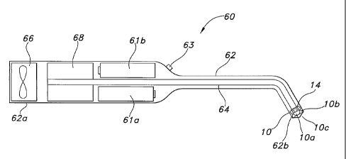
Referring to FIG. 6a, there is shown an LED curing device 60. The device 60 is
preferably a hand LED curing device. The device 60 includes a tubular wand
body 62 made
of plastic or metal having two ends a wide end 62a and a tip end 62b which is
bent. Please
1~
CA 02493130 2005-O1-20
WO 2004/011848 PCT/US2003/023504
note that the tip end 62b of the body 62 need not necessarily be bent. LED 10
is located at
end 62b of the body 62. A heat pipe 64 extending through body 62 is bonded
with glue or
solder inside the conductor slug 14 preferably of copper of the LED 10,
although no cavity or
hole need be made in the conductor slug 14. As shown in FIG. 6a, the heat pipe
64 may be
modified to "neck" down at the end 62b. Also a flattened heat pipe may be used
and the LED
is bonded on top of the flattened end. An optional battery pack 61a and 61b
may preferably
be driven by a wall plug transformer not shown, around middle portion of the
body 62. A fan
66 that is approximately 30 mm2 may be located at the end 62a of the body 62.
A heat sink
68 preferably of Al or Cu is glued to "cold end" of the heat pipe 64 between
the fan 66 and
the battery back 61a and 61b. The fan 66 is used to blow air over the heat
sink 68 and
exhausted through ports (not shown) in the body 62 that most components are
mounted in.
Switch 63 controls the electrical current to the LED via wires (not shown)
connecting the
battery pack 61a and 61b to the LED 10. The LED Tense l0a is shown surrounded
by
pambolic reflector lOb and optional additional Tense lOc. The heat pipe 64 is
a closed
container into which a small amount of liquid (working fluid, typically water)
is injected
under vacuum. The inner walls of the container of the heat pipe 64 are lined
with capillary-
action material (wicking structure). When a portion of the heat pipe 64 is
exposed to heat
produced by LED 10, the fluid in the heated portion i.e., hot end of the heat
pipe 64 vaporizes
picl~ing up latent energy. The vapor flows to the "cold end" of the heat pipe
where the vapor
cools and condenses releasing latent energy and the condensed fluid is
returned by capillary
action to the hot end. The heat pipe 64 serves as a heat engine taking heat
away from the
LEDs 10.
FIG. 6b is an expanded view of the tip end 62b of the device 60 in FIG. 6a.
The
"pocket" 65 is shown wherein the heat pipe 64 is milled, drilled, molded,
etc., in the slug 14
18
CA 02493130 2005-O1-20
WO 2004/011848 PCT/US2003/023504
of the LED 10 such that it is only a few .001's of an inch greater diameter
than the heat pipe
64. High thermal conductivity epoxy is placed in the bottom of the pocket 65
prior to the
insertion of the heat pipe 64. The operation of a heat pipe 64 is as discussed
above, known
by those skilled in the art of heat transfer but has not been used prior to
this invention in a
hand held LED device 60 for curing. Also in the prior art, the heat pipe 64
has not been
inserted into or onto the slug 14 or submount of an LED 10 as shown, and also
not used for
the purpose of mounting an LED 10 at the end of a wand 62 having a small
diameter of
around 8.5 mm Q~. Most LED slugs are glued or soldered to a large PCB board or
large, flat
heat sink which is incompatible with the application of the LED device 60
described herein.
It is understood that the heat pipe 64 could be soldered or glued to the LED
"slugs" without
the "pocket" 65 or a separate heat pipe could be bonded to the LED.
In the above discussed embodiment of FIGS. 6a and 6b of the present invention,
the
heat pipe 64 transports heat in a direction that is not substantially
perpendicular to the p-n
junction of LED 10. The end of the device of FIGS. 6a and 6b that includes the
LED 10 and
reflector 106 mounted on the tip of the heat pipe 64 and surrounded by a
sleeve, is bent at 45°
about 7 mm from the end of the device. The light is traveling away from the p-
n junction
plane in a substantially perpendicular direction, (if it were collimated,) but
the majority of the
length of the heat pipe, and therefore the direction the heat is transported,
is not perpendicular
due to the 45° bend in the heat pipe 64. If there were no 45 °-
bend (i.e. straight) the heat
would flow in a substantially perpendicular direction to the p-n junction.
FIG. 7 shows a liquid-cooled version of the LED hand held curing device 60. By
utilizing liquid cooling, the wand 62 (long, slim tube) may be made flexible
by using flexible
liquid carrying tubes. Wavelengths from 200 nm to 11,000 nm could preferably
be used
19
CA 02493130 2005-O1-20
WO 2004/011848 PCT/US2003/023504
including "white" LEDs. The LED body 10 is shown with an attached lense 10a.
The LED
is located at the end of wand 62 that is approximately 8.5 mm ~ and can be
flexible, semi-
rigid or rigid. Coolant tubes 34 (inlet) and 35 (outlet) are bonded to an
optional threaded
through the hole 67 in the slug of the LED 10. In this way coolant is passed
through the LED
10 at approximately 2 psi to 50 psi for the purpose of cooling the LED die
(not shown, but
bonded to one end of the conductor slug 14). The coolant tubes 34 and 35 are
attached
respectively to the pump 50 which supplies the coolant (i.e., liquid) and a
finned heat
exchanger 52, which receives the heat. Fan 66 is the drive electronics for
pump 50. Fan 66
passes air over the external fins of heat exchanger 52 and the air is
discharged through ports
(not shown) in the molded plastic housing of the body 62. No electrical leads
are shown for
drawing clarity. Battery pack 61a and 61b is shown. The device may be operated
strictly
from batteries or may have a cord to a wall mounted transformer. The purpose
of the liquid
cooling is to be able to remove the heat generated by the LED die 10 that is
in a very small
area and "pump" the waste heat to a larger area, the heat exchanger 52 via the
heat pipe 64.
Using this technique, LEDs may be driven at higher operating currents and
output power than
if they were mounted to a flat heat sink and/or PC board (PCB). Additionally,
it is difficult to
have a heat sink of PCB out at the end of an approximately 8.5 mm ~ diameter
wand that is
needed to get into "tight" spaces in an electronic assembly glue curing
application or a
patient's mouth for curing or whitening. Also very important, is the fact that
it is easy to
make "wand" that is flexible if liquid cooling is used to transport heat at
high flux from one
end of the wand to the other.
FIG. 7a is an expanded view of FIG. 7 wherein the inlet and outlet tubes 34
and 35
respectively, are more clearly shown. These tubes are available from HV
Technologies
(North Carolina) with a thin spiral or coil wire in the wall for lcinlc
resistance. 90° bent tubes
CA 02493130 2005-O1-20
WO 2004/011848 PCT/US2003/023504
71 and 73 are glued into the through hole 67 in the conductor slug 14 to pass
the coolant from
the inlet tube 34 into the LED 10 and similarly to send the coolant out of the
LED 10 into
outlet tube 35. The approximately 8.5 mm Q~ tube wand 62 may be rigid or
flexible
depending on the application. Curing industrial/photonic adhesives could be
accomplished
by using a flexible "mono-coil" type outer tube that would carry the coolant
tubes 34 and 35
and electric wires to the LED 10 at the end. The "mono-coil" would then serve
as a sort of
replacement for a light-guide for curing equipment. The LED 10 at the end
could also be
replaced by an edge emitting laser diode or VCSEL. The LED 10 may be driven at
higher
currents than would be possible with just a heat sink, and is especially
useful in small,
contained areas where it is difficult to cool high power density devices and
areas where a
flexible light source is advantageous.
FIG. 7b is an expanded view of another embodiment for the instant invention.
Here
the LED 10 has a coolant inlet hole 75 in the center of the conductor/slug 14
and a feeding
inlet tube 34 is shown. The inlet hole 75 is bi-sected by one or more outlet
holes 75a and 75b
near the bottom or end of the hole 75. This arrangement allows for lower
thermal resistance
cooling as the inlet hole 75 serves to "impinge" coolant on the area of the
conductor/slug 14
at the bottom of hole 75 that is immediately below the LED "die" (not shown
for clarity).
The outlet holes 75a and 75b (two more outlet holes are not shown for clarity)
allow the
heated coolant to escape with minimal back pressure where it is returned via
pump 50 to the
heat exchanger 52 (or chiller). It is understood that all these embodiments do
not necessarily
have to be hand held. A "5 W" LED may preferably be driven with two to six
times the
current with this technology. Multiple arrays or single LED 10 (or laser
diode) units may use
the same cooling techniques described in the instant invention for static or
stationary wall or
21
CA 02493130 2005-O1-20
WO 2004/011848 PCT/US2003/023504
bench-top units for may applications where a light source of high intensity in
a tight space is
required beyond just curing.
In an alternate embodiment of the present invention, there is provided a LED
device
wherein the LED die is mounted and/or bonded to the tip of a heat pipe, where
the heat pipe
may have the function of an anode or cathode in addition to its heat sinking
and transport
functions. This LEDlheat pipe invention has broad applicability when used with
UV or
visible LED packages and/or individual die or combinations of each such as in
UV lamps for
curing adhesives and various other applications.
Referring to FIG. 8, there is shown the heat pipe 64 having an average range
of the
diameter of preferably between 3 and 6 mm and average length preferably
ranging between
25 mm and 500 mm. The LED chip (or die) 10 is shown bonded to the tip of the
heat pipe
64. The heat pipe 64 may be flattened to accommodate the flat die. It is
understood that
packaged LEDs, i.e., presoldered to heat sinks or slugs could also be used. If
the conductor
slug 14 is used it may have a female contour in it to accommodate the end of
the heat pipe 64.
The heat pipe 64 itself may be the electrically charged anode 11 and a wire
bond may be
made on top of the LED die as shown in FIG. 8 to make the cathode wire
connection 12.
These functionalities could also be reversed. In this manner, the heat pipe 64
provides an
electrical connection to the LED 10 in addition to cooling the same. The heat
sink 68 may be
bonded to the condensing end of the heat pipe 64 and an optional fan 66 to
blow air serving
as the cooling medium over the heat sink 68.
In FIG. 8a, the heat pipe/heat sink is shown with multiple LED dies 10. They
may be
connected in electrical series or parallel or be individually addressable. The
dies 10 may emit
22
CA 02493130 2005-O1-20
WO 2004/011848 PCT/US2003/023504
one or more centered wavelengths. A shaped, molded or potted polymer or glass
or ceramic
lense 81 is shown and it may encapsulate the LED dies 10 and is preferably
made from a UV
degradation resistant polymer. The arrows 82 depict the light emission from
the LED(s) 10.
Element 84 depicts a vapor cavity that extends down the center of the interior
of the heat pipe
64. It is substantially parallel to the outside diameter sides of the heat
pipe 64. The LED
cathode and anode surfaces (p-n junction) are substantially perpendicular to
the heat pipe
vapor cavity 84 axis of the heat pipe 64 which is substantially straight and
unbent. The heat
pipe 64 may be bent in may different shapes for many lighting applications.
FIG. 9 is a hand held LED curing device 60 having a plastic housing that
incorporates
at least one LED die 10 or at least one pre-packaged LED device that is bonded
to the
evaporating end of a heat pipe 64. Cathode wire 12 is bonded to the cathode
side of the LED
die (not shown). Element 20 is a transparent material that is preferably a UV
resistant potted
or molded polymer as discussed and shown earlier in FIG. 2. Again, element 63
is the
electrical on/off switch. Element 92 is a surface including a gel material
that preferably
contains hydrogen peroxide and also preferably a photosensitizer,
photoinitiator, or
chromophor that the actinic light from the LEDs "activate". Element 94 is a
phase change
material that is preferably a paraffin material which is placed between heat
pipe 64 and the
rest of the part of the device outside the heat pipe 64. When the LEDs 10 are
turned on, the
waste heat will flow down the heat pipe 64 and melt the paraffin 94 after a
predetermined
approximate time. The paraffin 94 will melt, i.e. change from solid to a
liquid and expand
and "break" the electrical circuit that is formed between the batteries 61a
and 61b (which may
have a different orientation than shown, i.e., upside down) the electrically
conductive piston
96 and spring 98, the electrically conductive (preferably water filled copper)
heat pipe 64
(which, in essence becomes the anode), the LED die 10 (or pre-packaged LED
device) and
23
CA 02493130 2005-O1-20
WO 2004/011848 PCT/US2003/023504
the cathode wire 12. This phase change will help conduct heat away from the
condensing
end of the heat pipe 64. In this case, instead of fan, paraffin 94 will absorb
heat from the heat
pipe 64. Furthermore, paraffin 94 absorbs heat energy without raising
temperature when it
melts and cools down. Again, this process works best for short duty cycle
application. The
novelty of this embodiment is the ability to rapidly transport heat from the
LED 10 through a
heat pipe 64 past the batteries 61a and 61b and to a forced convection cooling
(or also non-
forced convection in another embodiment). For short duty cycle applications
the heat pipe 64
(preferably porous) can be surrounded by a phase change material, such as
paraffin, to absorb
heat as will be described in greater detail with reference to FIG. 9 below.
FIG. 9a shows an adhesive curing device embodiment of the present invention.
As in
other embodiments, a CVD Diamond heat spreader 230 as shown in FIG. 19, is
optionally
positioned between the LED 10 and the heat pipe 64 in the wand tube 62, which
is anodized.
If the anodized wand tube 62 is not used, the heat pipe 64 can preferably be
covered with
.002" thick polyester shrink wrap. Here, the heat pipe 64 functions as the
anode 11 to the
LED 10. LED 10 is optimally soldered to the CVD heat spreader 230 which in
turn is
conductively glued to the end of the heat pipe 64. Cathode wire 12 is bonded
to the LED 10
and the parabolic reflector 10b. As in other embodiments, a phase change
material 94
(usually paraffin) can preferably be communication with the heat pipe in order
to further
dissipate the heat being generated by the LED 10 and transported along the
length of the heat
pipe 64. Here, the phase change material 74 is also in communication with
copper wool 95,
which further dissipates heat throughout the phase change material 74 due to
the high thermal
conductivity of the copper wool. This embodiment is shown to include lithium
batteries 96
but, as in other embodiments, power could instead be supplied to the device of
the present
invention using a power cord of some kind.
24
CA 02493130 2005-O1-20
WO 2004/011848 PCT/US2003/023504
FIGS. 9b and 9c depict an LED array for use typically in ultraviolet curing
applications. This embodiment is composed of a number of LEDs 10 disposed upon
a slug
14 with a blind hole into which the heat pipe 64 is fixably and/or detachably
inserted. Fins
208 as more clearly shown in FIG. 12a are optionally included. Fins 208 are
preferably
bonded with solder 110 or a high thermal conductivity glue. The fins 208
further dissipate
the heat transferred from the LED 10 to the heat pipe 64. The LEDs 10 are
attached to the
slug 14 via bond pads 214 via bond wires 212 as more clearly shown in FIG.
14b, and may be
electrically powered in series, in parallel, or as individually addressable
entities. The number
of LEDs 10 that may be used in this type of an embodiment is limited only by
the size of the
slug 14 and the heat transport capacity of the heat pipe 64 in combination
with any other heat
dissipation mechanism (such as the fins 208). It is easy to envision an
embodiment wherein
the single heat pipe 64 is replaced by a number of separate heat pipes of
similar or varying
size, all of which are in communication with any number of LEDs 10 via a
single slug 14. It
is noted that two fins 208 are shown but more than two fins 208 are possible.
Positive 97 and
negative 97' gold contacts wrap around the edge of the slug 14. Also note that
LEDs 10 are
shown in series, but may also be in parallel.
In another embodiment, the device of the present invention is preferably used
UV
curing applications where the heat pipes are located in different orientations
wherein the hot
end has the LEDs and the cold end is in a heat sink. The heat pipe in these
embodiments is
somewhat analogous to the function of a light pipe or lightguide except that
it transports heat
instead of light, and the source of light is at the output tip of the heat
pipe.
In an additional aspect of the present invention, there is provided a device
used to cure
UV inks and coatings and adhesives. The device includes an array of large area
ITV (or
2s
CA 02493130 2005-O1-20
WO 2004/011848 PCT/US2003/023504
visible) LEDs that are mounted on heat sinks) which are cooled by an array of
(circular or
flat) heat pipes that are themselves cooled by one or more fans as described
in detail below.
Referring to FIG. 10 there is shown a device 100 having an array of LEDs 10
which
are soldered to one or more heat sinks 68, preferably formed of copper. The
heat sinks 68 are
electrically isolated from each other by thin strips of Kapton 101 or other
non-conductive
material that have thin layers of adhesive on both sides 102 and a layer of
copper foil 103
sandwiched in between. Each LED 10 has a wire bond 104 that attaches to the
copper foil
103 of the heat sink 68. All copper foil layers 103 are brought to form the
cathode common
electrical connection. For every approximately 11 mm of electrode length there
are three
approximately 3 mm Q~ blind holes 107 drilled in each electrode 109 (only one
of 90 are
numbered). An approximately 200 mm long by 3 mm ~ heat pipe 64 is inserted
with an
electrically conductive compound in each hole 107. The heat pipe condensing
(cold) ends are
inserted in a top plate 108 and attached with an electrically conducting
compound such as
conductive epoxy. This top plate 108 serves as the common electrical anode
connection.
Depending on the design of the LEDs the polarity of the electrical connections
can be
reversed or modified. The current path as shown, is through the top plate 108,
down the heat
pipes 64, through the electrodes 109, through the LEDs 10, through the wires
104, and out
through the copper foil 103. It is understood that electrodes 109 could be
monolithic with
circuit "traces" for a cathode connections, or they could be electrically
isolated from the heat
pipes 64 and the LEDs 10 could be bonded directly to the heat pipe tips
(ends), which is most
applicable if there is a through hole (rather than blind hole) in electrodes
109.
Glass may be ion beam sputtered over the LEDs 10 for index matching purposes.
Gold may be electroplated onto the copper surfaces for ease of wire bonding
and die bonding.
26
CA 02493130 2005-O1-20
WO 2004/011848 PCT/US2003/023504
A single point, diamond-turned, fly-cut pass may be made over the bonded three
electrodes
109 to create a small, flat, die-bonding surface. Lastly, a glass plate (cover
slide) may be
placed over emitting LEDs 10 to protect them. The glass may be hermetically
seated and
have a sub-wavelength structure on it for anti-reflection purposes. Also, flat
plates (thinner
than the top plate) can be installed to increase surface area. Preferably one
or more 100 mm
fans on each side of the heat pipe array cool the heat pipes in a push me-pull
me arrangement.
The optional flat plates can be oriented parallel to the airstream (from fans)
or blower(s)). It
is to be noted that in FIG. 10, the LED 10 repeat down length of device in
groups of six and
only 18 LEDs of approximately 540 LEDs are shown for drawing clarity. However,
different
quantity and sizes of LEDs 10 may preferably be used.
The heat pipes are preferably oriented vertically so that the wicking action
is
enhanced by gravity. The heat pipe (or heat pipes) may have an additional
bonded heat
exchanger (or heat sink) with fins surrounding it (for added surface area) or
it may be stand-
alone (no bonded heat sinks or fins). When an array of heat pipes are employed
each heat
pipe essentially becomes a "pin" in a so called "pin-fin" array heat sink to
dissipate thermal
energy from the LEDs over a large area. The heat is taken in by the heat pipe
64 at the end
where LED is placed and spread out in the entire surface area of the heat pipe
which
preferably is between 2-8 mm in diameter. In the preferred embodiment the heat
pipe
transports the heat away from the p-n junction of a diode in a direction that
is substantially
perpendicular to the junction. It must be stressed that because heat pipes can
be bent in most
any shape or form, it must be understood that the heat pipe could transport
heat in a direction
that is not substantially perpendicular to the junction. The vapor cavity in
the heat pipe may
have only a portion that is nearly perpendicular or nearly parallel to the p-n
junction. Also,
only a portion may be nearly perpendicular or nearly parallel to the emitted
light from a light
2~
CA 02493130 2005-O1-20
WO 2004/011848 PCT/US2003/023504
emitting device. The aforementioned word "nearly" may be substituted with
"substantially".
Also, the term "heat" can be used interchangeably with "waste heat", "thermal
energy", etc.
One or more heat pipes (arrays) cooling one or more, light emitting devices
(arrays) may be of
small (preferably less than 2" square inches) of large (preferably more than
2" square inches)
dimensions thus used for a variety of medical and industrial uses such as
curing adhesives.
For curing adhesives, an apparatus similar to FIG. 10 is ideal for all
applications that a
microwave (electrodeless) lamp is currently used for.
The inner diameter ("ID") along the length of the heat pipes is comprised of a
hollow
vapor cavity 84 as shown earlier in FIG. 8. The light from the LEDs is
generated at the "p-n"
junction which is epitaxially grown in layers on a preferably GaN wafer which
is diced into
chips. The chips may be bonded to the electrodes "p" side down. Other wafer
types are SiC
and sapphire. Other means for forming p-n junctions other than epitaxial may
be employed.
Different styles and sizes and manufacturer of LEDs may be substituted for
those described
and depicted in the figures. As discussed earlier, the cold ends of the heat
pipes 64 can be
cooled by a coolant (liquid or gas). The electrodes 109 could also be liquid
cooled and have
internal channels therein.
In an additional aspect of the present invention, there is provided a novel
LED
packaging scheme and process for making same which results in a very simple,
inexpensive
and compact package. This advantageously allows the rapid transport of thermal
energy
away from a high energy density heat source such as an LED chip, to a very
large surface
area heat sink while minimizing the size of the heat source and the frontal,
cross-sectional
area of the heat sink surrounding it. This fast thermal transport most
preferably allows the
operation of LED chips) at a threefold to fivefold (or more) increase in power
over standard
28
CA 02493130 2005-O1-20
WO 2004/011848 PCT/US2003/023504
packaged chips while keeping the operating (junction) temperatures well within
rated limits.
Also, since brightness can be defined as the "power per solid cone angle of
light," when
increasing the chip power while maintaining the same cone angle, brightness is
increased.
This invention combines high brightness LED chips and highly effective heat
pipes in a novel
packaging scheme and process for making same which results, not only in the
ability to
operate the LEDs at unprecedented brightness, but also unprecedented cost per
watt.
Essentially, one chip is outputting the power of three to five chips (or
more), not in the area
of three to five chips, but in the area and cone angle of a single chip, with
minimal heat sink
area consumed around the periphery of the chip. This small frontal cross-
section results in
the ability to use compact and efficient lenses and reflectors that can take
advantage of the
chip's brightness in the most efficient, effective and space saving way
possible. The devices
depicted in this application may contain at least one infrared ("IR") die and
the emitted light
may be used for curing adhesives or coatings by heat instead of the more
common W or
visible photoinitiated chemical reaction. The LEDs may be used individually or
in array
form with one or more heat pipes either in a unit that is hand-held, fixed, or
some
combination of both. The present invention most preferably combines mainstream
IC
packaging technology, circuit board technology, and power LED technology in a
novel
configuration that provides solutions to a broad array of light curing
applications and devices.
These applications and devices advantageously utilize the primary attributes
of the
technology which is high brightness and power in a very compact and cost
effective package.
Referring to FIG. 11, there is shown a LED 10 bonded to the tip of at least
one heat
pipe 64. The LED(s) 10 is(are) affixed to the heat pipe 64, by a solder or an
adhesive 110
such as indium or tin, leadltin, or goldltin that is preferably
electrolitically deposited to the
29
CA 02493130 2005-O1-20
WO 2004/011848 PCT/US2003/023504
heat pipe 64. The solder process my use flux or be "fluxless". The square (or
other
geometrical shape) is defined by an exposed and developed area of the
electrophoretic
photoresist 111. The flux process must be compatible with the photoresist.
This photoresist
layer 111 also acts as a dielectric (insulating) layer. The heat pipe 64 is
adhesively bonded to
the inner diameter of tube 112 comprised of conductive material, preferably
aluminum. The
tube 114 may be anodized and it can act as the cathode to the device when the
wire 113 is
bonded or mechanically affixed to it in an electrically continuous manner. The
diamond-
turned or injection molded elliptical or parabolic total internal reflection
("TIR") reflector
10b is placed over the LED 10. It has an index of 1.53. The TIR reflector may
be a
Dielectric Totally Internally Reflecting Concentrator (DTIRC), a Compound
Parabolic
Concentrator (CPC), an Elliptical Concentrator (EC), a Compound Elliptical
Concentrator
(CEC), or a Compound Hyperbolic Concentrator (CHC). All of these may have flat
or
curved exit apertures. If curved, an aspheric surface may be employed. If
flat, a diffractive
surface may be employed. These reflectors also have the unique ability to mix
multiple
wavelengths that may be emitted from multiple light emitting devices into a
homogeneously
mixed beam of light. We refer to this unique attribute as a "color-mixing TIR"
reflector. The
space for the LED 10 is an integrally molded, concave female preferably
hemispherical
surface 114 that is filled preferably with a high index silicone polymer or
other transparent
material. This high index polymer may preferably be ~1.6 or greater. The
refractive index
between reflector lOb and the surface 114 can preferably add optical power and
bend light
rays to stay within the critical angle for TIR. An anti-reflection (AR)
coating may be ion
beam sputtered (or other process) on the plane (or curved) emitting surface of
the TIR
reflector lOb. The vapor cavity 84 of the heat pipe 64 is shown and is only
approximated. In
the preferred embodiment of the invention, the heat pipe 64 of a conductive
material,
preferably copper, may act as the anode (although it could be cathode or even
electrically
CA 02493130 2005-O1-20
WO 2004/011848 PCT/US2003/023504
neutral or some combination of all three). A conduction path can be traced
from the batteries
(not shown), through the heat pipe 64, through the solder 110, through the LED
10, through
the wire 113, into the insulated sleeve tube 112, and back to the batteries
(not shown) through
the electrically conductive heat sinks) (not shown) after passing through a
switch (not
shown). The wire 113 is bonded to the inner diameter of the insulated sleeve
112 with a
small dot of electrically conductive adhesive 115. FIG. 11 depicts only one
LED die 10 but
multiple LEDs 10 at the same or multiple or varied wavelengths may be
employed. The
dielectric layer 111 electrically insulates the electrically active heat pipe
64 from the
electrically active sleeve 112. The sleeve may be desirably anodized aluminum
with an
unanodized spot underneath glue dot 115 so as to form a current conduction
path from the
wire 113 to the tube 112. A small gap 116 may or may not exist and it may be
filled with a
material such as thermally conductive or thermal insulating adhesive. This may
be
advantageous if the tube 112 and heat pipe 64 are bent near the tip at an
angle of
approximately 30° to 45°. The wick structure 127 shown in FIG. l
if is preferably small,
axially extruded grooves but it may be a screened-wick or sintered (powdered)
metal wick.
An AR coating or sub-wavelength structure may be employed on the exit aperture
118. LED
light emission is depicted by arrows) 117 which are shown undergoing TIR at
the reflector
wall/air interface. Light emitting from aperture 118b is depicted by arrows)
118a. The light
118a is then impinging on the example application of two blocks 119 and 120
with light cure
adhesive. The light is of sufficient intensity to "cure" the adhesive 121 and
the two blocks
119 and 120 will be affixed together by the cohesive strength of the adhesive
121. The
adhesive curing device in FIG. l la may be used to cure "surface coatings"
such as UV clear
coats, conformal coatings, etc. The device may also be used to cure "solid-
body" objects
such as those found in stereolithography processes or casted or molded
objects. Examples of
31
CA 02493130 2005-O1-20
WO 2004/011848 PCT/US2003/023504
these "solid-body" objects are the bases and/or ear molds for hearing aids as
well as countless
applications involving photochemical curing of molded object in transparent or
open molds.
The LED 10 bonded onto or near the tip of at least one heat pipe 64
simultaneously
maximizes the rate of heat transfer away from the LED chip 10 and minimizes
the frontal
cross-sectional area of the heat sink 68 or submount or heat exchanger. The
light emitting 82
from the LED junctions) 10 preferably travels in a direction that may be
substantially
opposite to that of the waste heat that is transported axially down the length
of the vapor
cavity 84 of the heat pipes) 64 and away from the junction(s). The light from
the device
may emit into a shaped volume that is substantially opposite to a shaped
volume of material
which the heat is dissipated in or transported to. The plane that separates
these two volumes
may be the p-n junction plane (the transition boundary between p-type and n-
type materials in
a semiconductor) and/or it may be the plane that the epitaxial p-n junction is
bonded to.
Because the heat preferably is not distributed over a large radial distance,
but rather a large
axial distance, close spacing of LED or LED assemblies (or an array of
assemblies) as well as
their associated optical systems (lenses, reflectors, etc.) and heat
exchangers may be spaced
closely together. This results in high power LED devices and/or assemblies
that are more
compact, lightweight, and inexpensive to manufacture than conventional
devices.
It has not been shown in the previous art to place a heat source such as a
diode (or
other high energy density semiconductor device) on the tip of a heat pipe
because it has been
considered sub-optimal. The reason for this is that it has been thought to be
best practice to
place the heat pipe into a larger heat sink with the heat source bonded to
this heat sink so as
to allow the heat sink to spread the heat around and along a larger surface
area of the heat
pipe. The problem with this is that there is generally more material between
the heat source
32
CA 02493130 2005-O1-20
WO 2004/011848 PCT/US2003/023504
and the heat pipe and the heat must travel through this excess material to
reach the heat pipe
itself, as well as travel around the circumference of the heat pipe. Also, the
heat will spread
both toward and away from the cold (heat exchanger) end because the source is
not at the tip
of the hot end. All this imparts a great deal of thermal resistance between
the heat source and
the heat exchanger. Also, if a small high power density device (like a diode)
is placed near
the wall of the heat pipe it can "dry-out" i.e., deplete the wick structure of
fluid of a localized
area. By placing the die, such as a light-emitting diode 10, on the tip of the
heat pipe 64, as
shown in FIG. 11, there often is not a functioning wick structure immediately
below the die,
and so dry-out may be less of an issue. Most importantly, a full 360 ~ heat
spreading around
the heat pipe 64 is easily accomplished in a radially and circumferentially
uniform manner,
thereby decreasing the likelihood of dry-out as thermal energy moves along the
wick
structure. The LED 10 (heat source) is at the hot (evaporating) end of the
heat pipe 64 at the
furthest possible point from the cool (heat exchanger) end of the heat pipe.
The cool end is
also known as the "condensing" end. Additionally, if the heat pipe 64 is at an
angle so that
the heat source at the tip is closer to the ground than the cool (heat
exchanger) end, then the
heat source has the benefit of being fed coolant (i.e., water) that is aided
by the force of
gravity as discussed above. This coolant may pool or form a reservoir that is
a ready source
for the wick structure due to evaporation that consumes liquid from the wick
structure. This
process decreases the likelihood of the dry-out phenomenon. Lastly, by bonding
the heat
source directly to the heat pipe 64 without a heat spreader or heat sink there
is one less
thermally resistive bond line for the thermal energy to travel through before
reaching the heat
pipe 64.
FIG. 11a is similar to the structure shown in FIG. 11, further including
electrically
conductive washer 122 that wedges the wire 113 against the inner diameter of
the sleeve 112.
33
CA 02493130 2005-O1-20
WO 2004/011848 PCT/US2003/023504
Incidentally, the sleeve 112 may be plastic with a metal conductive strip
adjacent to washer
122 or it may be a conductive metal with an electrophoretic coating to protect
it from the
environment. The electrophoretic coating would have a bare spot where the
washer 122
contacts the sleeve 112. Similar to FIG. 11, light emitting from the exit
aperture is depicted
by arrows) 118. In the example application the light 118 is shown impinging on
surface
mount device 123 and its lead with solder bump 124 as shown in FIG. 11a. The
light may
have an IR wavelength (could also have UV, visible, or other). In this
application, the solder
bump 124 will reflow from the heat of the light 118. The solder bump 124 may
instead be a
light cure adhesive bump or a heat cure adhesive bump, and may or may not have
a solder or
flux component in it. The LED light (as in all embodiments) may instead be
emitting from a
laser diode. If the light is emitting from a laser diode, it may preferably be
focused to a very
small spot. A visible component of light (perhaps from an LED) would be
preferred if the
actinic light was invisible (i.e. UV or IR). This nearly point source of light
may be used for
other applications, as well as for heating, surface modification (i.e.,
ablation, etc.) or photo-
chemical reaction, etc.
FIG. l lb depicts another embodiment of the invention for mounting the LED(s)
10 in
the center of the heat pipe 64. The Kapton or other non-conductive material
ring 125 is
coated preferably with copper on the top surface 126 of the ring 125. The ring
125 has a
shape, preferably a square shape cut out in the center which allows for proper
die positioning
when an external sleeve just bigger than the heat pipe 64 diameter is
positioned around it. A
solder reflowing operation may be undertaken and when the solder 110 (that may
be already
coated on the bottom of the die 10) is reflowed, the ring 125 will keep it
centered on the heat
pipe 64. The 'wire 113 that is bonded to the center of the die 10 is also
bonded to the top 126
of the ring 125. The conductive copper (or other conductive material) on the
ring 125 has
34
CA 02493130 2005-O1-20
WO 2004/011848 PCT/US2003/023504
perforations 125a that allow it to bend into a myriad of "fingers" when a
conductive sleeve
112 in FIG. 11c is brought into contact with it, thereby forming a current
conduction path
from the heat pipe 64 up through solder 110 and die 10, through the wire 113
into the copper
surface of the LED 10 and then into the sleeve 112 of FIG. 11. An adhesive
such as glue 115
may exist below or on ring 125.
FIG. l lc is similar to Drawing l lb, except that the conductive sleeve 112 is
shown
making contact with the conductive ring 125. The sleeve 112 may be anodized
aluminum
except a small area may be masked during the anodizing operation to allow an
exposed
electrically conductive area that can contact ring 125. Instead of anodizing,
an
electrophoretic coating may also be employed.
FIG. l ld further depicts the heat pipe 64 with the solder 110 and the LED die
10 on
top and in the center of the heat pipe 64. The wire 113 is bonded to the
center of the die 10
and also is bonded to the top of the copper strip or Kapton ring 125 that has
an adhesive
section 115 between it and the heat pipe 64. The current connection between
the dies) 40
and the sleeve 112 is made when the copper strip/Kapton ring 125 contacts the
sleeve 112
which is connected in a current conduction path to the battery(s) or power
supply (not
shown). The die 10 may be centered by a manual or computer driven die bonder
or a pick
and place machine, with or without machine vision. This is true with all dies)
depicted in
this invention.
FIG. l le shows the sleeve 112 as a separate heat sink 68. The LED 10 is shown
with
attached wire 113 mounted on the tip of the heat pipe 64. The sleeve 112, the
heat sink 68
and the heat pipe 64 may preferably be electrically isolated from each other
and may be any
CA 02493130 2005-O1-20
WO 2004/011848 PCT/US2003/023504
polarity, or neutral, or a combination of polarities. They may also carry
electrical traces that
can be individually addressable and traced to individual dies.
FIG. l if further shows the heat pipe body 64 with sintered wick structure
127. In this
application, the wick structure 127 is shown with a full coverage of operation
wick structure,
not only along the inner diameter circumference walls, but also completely
covering the tip
body surface under the die 10 at the hot end of the heat pipe 64 shown in this
drawing. The
solder 110 or conductive epoxy is shown as well as wire 113 which is bonded to
die 10. If a
thermosetting adhesive exhibiting a high thermal conductivity such as one
disclosed in U.S.
Patent No. 6,265,471 is used, it is preferred to first deposit silver (Ag) to
both the die 10 and
surface of the substrate (or any two contacting surfaces) it is bonded to as
this greatly
decreases the contact thermal resistance (interfacial resistance) because the
patented
formulation of the adhesive allows fantastic heat transfer between silver-
silver connection
and worse performance with contact between other material.
FIG. 12 shows an exploded view of the LED/heat pipe assembly as it is
assembled
into one or more heat sink 68 with battery pack 61a/61b. The heat sink is
actually two
electrically isolated heat sinks 68a and 68b that when "shorted" by switch 63
complete an
electrical circuit from the positive battery lead that contacts the tip
opposite the LED 10 of
the copper heat pipe 64, through the LED 10, solder and wire path 201, through
the sleeve
112 into the cone section of the heat sink 68, through the closed switch 63
into the bottom
section of the heat sink 68, through the battery pack 61a/61b and into the
cathode end of a
battery (or batteries) 202. The two heat sinks 68 may preferably be anodized
aluminum or
some other conductive material that may be electrophoretically coated with a
non-conducting
polymer. The two heat sinks 68 may be bonded together with non-conducting
adhesive (not
36
CA 02493130 2005-O1-20
WO 2004/011848 PCT/US2003/023504
shown) and the heat pipe 64 through hole 203 may be filled with an
electrically insulating,
but thermally conductive compound. The heat pipe/sleeve assembly may be held
in place in
the heat pipes by a simple set screw 204. The hole 203 is simply a long hole
through each
heat sink 68a and 68b that accommodates the heat pipe 64 and it may or may not
have a
dielectric layer. The fins 218 shown in FIG. 12b on the heat sinks) 68 may be
either radial
and/or at an angle in relation to the heat pipes and for they may be axially
disposed.
The light from the LED 10 emits through a transparent dielectric concentrator
205.
The light emission direction is shown by arrows 206. The most preferable
embodiment
contains one high power LED 10 on the end of the heat pipe. However, multiple
LEDs 10
cari be used at one or more centered wavelengths. Also the LED(s) may
preferably be
mounted on a small heat sink or heat spreader that is in turn mounted near or
on the end of
the heat pipe. Multiple heat pipes may also be employed. Individual or arrays
of lenses may
also be employed. If the lense is a reflector it may be faceted or it may have
smooth walls. It
may be totally internally reflecting or it may be a metallic or dielectric
coated wall or
polished wall reflector.
FIG. 12a shows the light emitting diode 10 through reflector/lens l0a/10b. The
sleeve
112 (not shown) is electrically connected to heat sink 68a. Switch 63
completes the electrical
circuit between electrically conductive heat sink 68a and heat sink 68b.
Battery pack 61a/61b
is also electrically active (current carrying) and its function, beyond
containing the batteries is
to connect the cathode end of the battery 202 in the heat sink 68b. Also, O-
ring 207 is shown
and is attached at the connection of the heat sink 68b and battery 202 to seal
out water and to
provide a smooth (tactile) feel during the thread rotation action. The light
emitting device 10
shown in to FIG. 12a may preferably be powered by an electric cord. The device
may be
37
CA 02493130 2005-O1-20
WO 2004/011848 PCT/US2003/023504
convective cooled through the many fins 208 as will be shown in FIG. 12b. The
device may
have a gravity or tilt-type shut-off switch as will be shown in FIG 12c within
the handpiece
shown to prevent the device from being operated in a substantially non-gravity
aided wick
orientation. Furthermore, the device may further desirably have the heat pipe
68 and sleeve
112 together bent at an angle.
FIG. 12b depicts a solid-state lighting application wherein at least one LED
die 10 is
bonded to at least one heat pipe 64 which is then further bonded to at least
one or more heat
sinks 68. In the preferred embodiment, the heat pipe 64 is oriented
substantially down or
vertical with the LEDs 10 being at the lowest point near to the ground. In
this way the heat
pipe 64 is said to be aided by gravity. The LED/heat pipe assembly is the same
assembly
depicted in FIG. 11a, except that the heat pipe 64 is shown bonded in the
somewhat
spherically shaped heat sink 68 that has fins 208 that may be machined, or
most preferably
molded in place. If it is molded it may be thixoformed, die cast, permanent
molded, or other
similar process. These processes facilitate the high volume and low cost that
is needed for a
solid-state lighting product. All heat sinks 68 or heat exchangers 76 in this
application may
be molded and may be made from an alloy of magnesium. It is understood that
multiple LED
dies 10 at multiple centered wavelengths and with heat pipes 64 (that may be
bonded in one
or more heat sinks) may be used. The LEDs 10 may be electrically individually
addressed
and individually modulated or they may be in electrical series, parallel, or
other electrical
connection. Threads 209 on top portion of the heat pipe 64 may be an
electrically "active"
component and they may facilitate an anode or cathode or ground connection. If
the heat
sink 68 is dielectrically coated and the threads are uncoated, they may be of
monolithic or at
least of electrically continuous design. Electrical contact 210 above the
threads 209 which is
preferably the cold end tip of the heat pipe 64 is either the anode cathode or
ground, but is of
38
CA 02493130 2005-O1-20
WO 2004/011848 PCT/US2003/023504
preferably the reverse polarity of the threads 209 and electrically isolated
from it. An
electrical circuit could preferably be placed between electrical contact 210
and the power
source such as within the threaded area 209 that may step up or step down
current or voltage.
This circuit may be present in any embodiment in this patent application. The
device
depicted in this drawing could be threaded into a heat sink 68 that may be
electrically active
and could absorb heat, as well as supply electricity.
FIG. 12c depicts the front section (light-emitting end) of the light source
embodiment
of the present invention. This light source may be portable and fit easily in
the human hand.
Again, like most embodiments in this patent application, a heat pipe 64 (or
heat pipes) is (are)
used to distribute heat rapidly away from an LED 10 (or LEDs) to much larger
fins on a heat
sink 68. A reflector lOb is shown and this reflector may be made adjustable in
that the cone
angle of light 211 may be adjusted by the operator or during manufacture of
the light source.
Wire bond 212 is shown running from the dies) 10 to the heat sink 68. The heat
sink 68 may
be anodized aluminum thereby shielding the operator form potentially adverse
electrical
shock because anodize (aluminum) is a very good electric insulator. The wire
bond 212
obviously contacts a spot on the heat sink 68 that is not anodized (masked
during
manufacture). The light source 211 may preferably have a rotating battery pack
that opens or
closes the electrical circuit when rotated approximately one-quarter turn.
FIG. 12d shows the entire light source whereas FIG. 12c showed only the front
section referred as the "nose" section. The LED light is shown emitting light
out of the nose
by arrows 211. Heat sinlc(s) 68 are preferably connected electrically by
switch 63. The
battery pack 61a/61b preferably is affixed to heat sink 68 by mechanical
threads (not shown)
in an electrically continuous manner.
39
CA 02493130 2005-O1-20
WO 2004/011848 PCT/US2003/023504
FIG. 12e depicts a heat pipe 64 and surrounding sleeve 112 bent at an angle,
which
could be useful to many of the embodiments described herein.
FIG. 13 shows the embodiment of the invention wherein multiple LEDs 10 are
bonded to at least one heat pipe 64 and rested on a circuit board 216. The
LEDs 10 are
individually addressable and at least one wire 213 is bonded to each LED 10
and the other
end of each wire 213 is then bonded to electrical bond pads) 214. These bond
pads 214 are
electrically isolated from each other. In this drawing the LED(s) 10 are shown
with an
electrically active heat pipes) 64 although electrically neutral heat pipes)
may be used in
this embodiment as well as any other embodiment in this patent application.
The heat pipe
64 may be a common anode 11 and each LED 10 would then be controlled by
varying the
resistance of a resistor located between the die/wire bond and the power
supply cathode. If
the heat pipe 64 is a common cathode 12, then the current leading to each die
10 may be
modulated directly (i.e., pulse width modulation and/or direct current
modulation). This
figure depicts a total of nine LED die. Any number of die from one to over one
hundred by
be employed. Also, any number of centered wavelengths from one to more than
one hundred
may be employed. Most preferably, wavelengths from the UV to the IR are used,
with 400
nm to 700 nm being the most preferable. This wavelength range may be used in
other
embodiments in this application. The TIR reflector lOb is also shown. It is
held in place by
lens holder 215. The circuit board and/or circuit board holder 216 is shown on
which the lens
holder 215 is placed. The hemispherical concave surface 114 in the reflector
10b is shown.
It is preferably of a higher refractive index than the material used in TIR
reflector 10b so as to
allow more light to escape the chip, due to TIR in the chip. Also, light rays
may
advantageously be bent at hemispherical concave surface due to refraction
caused by the
differing refractive indices. Aspherical, parabolic, elliptical, hyperbolic or
defractive surfaces
CA 02493130 2005-O1-20
WO 2004/011848 PCT/US2003/023504
may be substituted for the hemispherical surface. The outside diameter of the
heat pipe 64 is
shown in the drawing by the solid line drawn in a circle on the left. The nine
LEDs 10
depicted in the figure may be an assortment of red, blue, and green emitting
LEDs. It is
understood that instead of three LEDs of each color, only three LEDs total may
be used (i.e.,
one green, one blue, and one red). In the figure, rectangular (or other shape)
strips of each of
the three primary colors could take up the space of three of the nine squares
shown in the
LED 10. In other words, each of the three primary colors may take up one-third
of the
available (depicted) die space. This in some way might imply equal impedance
for a given
die area for each color, although this might not be true in all cases. Any
organic and/or
polymer LEDs could be employed in any embodiment of the invention. Red
inorganic LEDs
may preferably be used that are smaller in area than the blue or green LEDs.
Also, due to the
human eye's ability to detect different colors at differing apparent
intensities (i.e., sensitivity)
more red than green, and more blue than green LED area may preferably be
employed.
FIG. 14 depicts the device of FIG. 13 in an array formed of more than one
device of
FIG. 13. Actually, in FIG. 14 an array of only three devices are shown for
clarity. Between
each heat pipe 64 is shown the circuit board 216. This circuit board may be of
the
conventional epoxy laminate and/or it may be of solid conductive material such
as aluminum
or copper with or without a non-conductive polymer or ceramic layer
(laminate). It may also
be wholly or partially ceramic, such as BeO, alumina, A1N, or other. Circuit
traces such as
thin copper or gold or plated gold may connect wire bonds 213 leading from the
LED die (or
dice). The lenses l0a may touch each other and be circular at the contacting
final emitting
surfaces or they may be molded into a square shape at the final emitting
surface and therefore
have no "spacing" between them. Also, a final lens element (or elements) may
preferably be
employed after the final emitting surface for the purpose of further beam
shaping or
41
CA 02493130 2005-O1-20
WO 2004/011848 PCT/US2003/023504
environmental protection. Additionally, circular holders may be employed
around the lenses
10a.
FIG. 14a is similar to the cross-sectional view of arrayed devices of the FIG.
14 with
the addition of holders 98 as shown around the individual lenses or reflectors
l0a/b. Such
holders could be of any shape and size sufficient to support the individual
lenses l0a or
reflectors lOb.
FIGS. 14b, 14c and 14d depict different "pixel" spacing and geometric
patterns. A
"pixel" in this case is a heat pipe 64 with the nine (or other number) shown
LED(s) 10 on it.
Each heat pipe itself may be individually addressable as well as each
individual LED die on
each heat pipe or some other combination. The ring 125 shown around each heat
pipe may
"nest" in a circuit board as shown in the FIG. 14e. The heat pipes 64 are
shown for clarity.
The wires 213 are bonded to electrically isolated bond pads 214. When the ring
125 is nested
in a circuit board, a means for connecting circuit board traces to the
respective bond pads 214
on the ring 125 must be employed. This means may be accomplished by contacts
connected
by traces and plated through vias. The LEDs 10 may then be controlled by the
voltage and
currents that are applied to them from the traces on the board (connected to a
power
source(s)), through the wires 213 and then to the LEDs themselves. The wires
213 may be
attached (as in all embodiments) to the dies) 10 by a wedge, ball, or other
bond. Wedge
bonding is preferable because the wires stay more parallel to the board
surface. Ball bonds
can be advantageous in that the wire sticks out vertically from the chip and
tends to attract the
die encapsulating polymer in a manner that pre-wets the chip and greatly
reduces the
formation of bubbles as the lens or reflector is slowly lowered over the
die(s).
42
CA 02493130 2005-O1-20
WO 2004/011848 PCT/US2003/023504
FIG. 14e shows the blind female recesses in the circuit board that accommodate
the
rings 125 from the devices shown in FIGS. 14b, 14c and 14d. Contacts, vias,
and traces are
shown. The preferably blind female recesses) 217 in the board 216 are shown.
There are
also preferably blind female recesses) 217' depicted by dashed lines in the
board(s)that
accommodate the heat pipes) 64. There is a thin section of preferably board
material that is
of high thermal conductivity between the two blind holes or recesses 217 and
217'. In the
preferred embodiment, 217 and 217' are substantially co-axial; however this
need not be the
case. There may preferably exist a board laminate 218 preferably bonded on
board 216. In
this embodiment of the invention as shown in FIG. 14e, the recesses 217 are
actually through
hole(s). Bond pads 214 that are aligned in FIG. 14b are shown with circuit
traces on board
216. It is important to mention that through wires 213 under bond pads) 214 in
FIG. 14b are
not shown in the figure but must be present in order to make contact with bond
pads) 214.
The rings 125 from FIG. 14b may be square (or some other geometrical shape)
and would be
accommodated by a like shaped recess 217'.
FIG. 14f shows a device somewhat similar to the one in FIG. 14b. It shows the
heat
pipes) 64 co-axial to a hole through board 216. Board 216 could be a "ring"
similar to the
ring 125 in FIG. 14b. The board 216 is shown with a thin wall surrounding the
multiple dies
10. In this drawing, the dies 10 are shown in a "p"-side up embodiment. The
active epitaxial
layer is depicted on the top edge of the die 10. May different LED or laser
diode structures
and designs may be employed in all embodiments. In particular, LEDs with an
optically
resonant structure may be used, as well as LEDs or LDs that utilize "quantum
dots". Hole
219 is shown in the board 216 and wires 213 are shown leading from the
individual die 10 to
their respective bond pads 214 and then to respective circuit traces 220. The
heat pipe 64
may or may not be electrically active. If it is active, it may be the common
cathode and have
43
CA 02493130 2005-O1-20
WO 2004/011848 PCT/US2003/023504
an electrical connection to the wire 213 in the board 216. Wire 213 may be
conductive
adhesive connecting the heat pipe 64 to the circuit trace 220. Reflector lOb
is shown. Light
emission is shown by the arrows pointed upward. The board 216 may be affixed
to a larger
board with hardware or some passive locking arrangement to that individual
LED/heat pipe
assemblies may be changed as they wear out or technology warrants. Assemblies
with
multiple LEDs at multiple centered wavelengths in or near the visible spectrum
as depicted in
this figure and embodiment as well as others in this patent application are
ideal for automated
stage light assemblies, due to their compact, light weight, and high optical
power, which may
preferably be computer controlled to change color, intensity, hue, etc.
FIG. 14g shows heat pipe 64 inserted in a through the hole 219 of board 216.
Reflector lOb is shown with LED dice 10. A two part laminated board with
traces between
the layers is depicted as top layer 216a and bottom layer 216b. Wires 213 in
board 216 are
shown as wires making electrical continuity between the traces 220 sandwiched
between
layers 216a and 216b and the traces 220 on top of 216. It should be noted that
layers 216a
and 216b, comprising the circuit board 216, are optional in that the light can
function without
a circuit board 216 and another means of connecting wires from a power supply
to the bond
pads 214 can be employed in various applications. Again, fins may preferably
be attached to
the heat pipe 64 to employ convection or forced air cooling.
FIG. 15a shows four "pixels" (LED(s) on heat pipe devices) that are arrayed on
a
circuit board. Only four devices (each considered a "pixel") are shown in this
drawing for
purposes of clarity. Actually, an array of pixels such as 48 by 64, or 48 by
32, or 24 by 16 for
example may be employed. Examples of pixel spacing preferably might be center
to center
spacing of 12 mm, 18 mm, 23 mm, 35 mm or 50 mm. Provisions for adjustment for
44
CA 02493130 2005-O1-20
WO 2004/011848 PCT/US2003/023504
uniformity, dimming, brightness, hue, color space conversion and gamma
correction may be
employed. A portion of the circuit board 216 is shown. On the tip of the heat
pipe 64 nine
individually addressable LEDs 10 are shown. Each of these LEDs 10 have a wire
that
connects to a bond pad 214 on the circuit board 216. Please note that in this
embodiment
there is not a separate ring 125 as shown in FIGS. 14b, 14c, and 14d. The
wires 213 in this
embodiment lead from the separate LEDs on the heat pipes) to separate,
permanently affixed
bond pads 214 on the circuit board 216. Only one wire 213 in the entire
drawing is shown,
for clarity, as well as only one abbreviated circuit trace 220. It should be
obvious to those
skilled in the art to connect individual wires from individual LEDs to
individual bond pads,
and then these bond pads to appropriate circuit traces to light up the LEDs.
Note how the
multiple heat pipes 64 form a "pin-fin" type heat sink. All of the
circumferential surface area
of the heat pipes is used to conduct heat to the ambient air that flows either
by natural or
forced air convection between the pins (a.lc.a. heat pipes) and the heat pipes
may have fins
attached in any orientation to further increase surface area. The space
between the heat pipes
allows air (or other medium) to circulate and cool the heat pipes. The fins
could actually be
all monolithic in a honeycomb-type design wherein the bare heat pipes slide
into holes in the
all monolithic honeycomb heat sink. This heat sink maybe made of any thermally
conductive
material, and it may or may not be forced air cooled. If the fins are not
monolithic, but are
joined to heat pipes, they may be at a 45° angle (or so) to the heat
pipe orientation, as well as
at a 45° angle (or so) to the horizon to facilitate naturally
convective flow of air because heat
will rise up through the fins and draw cool air in behind. Also, the air will
be forced to
impact the fins more directly than if they fins were mounted perpendicular
(vertical) to the
horizon. As in all embodiments in this application the heat pipes may have
some other
working fluid than water or may have some other substance added to the water.
In an
alternate embodiment, for example, alcohol (glycol, methanol, etc.) may be
added to protect
CA 02493130 2005-O1-20
WO 2004/011848 PCT/US2003/023504
from freezing. Also, other materials, such as aluminum, could be used instead
of, or in
conjunction with copper for the body (wall) or heat pipes. Lenses l0a are also
shown. These
may be of the TIR variety or refractive, diffractive, reflective, or a
combination. When the
LEDs 10 on one of the heat pipe 64 are turned on in some combination, the
pixel can be
thought of as "on" or "active". In general, each heat pipe's LEDs would be
some combination
of individually addressable red, blue, and/or green LEDs. As in all
embodiments in the
application "white" LEDs may be employed.
FIG. 15b an array of heat pipes 64 that are inserted and bonded in blind holes
in a
board 216. The blind holes 221 are more clearly shown in FIG. 15c. The board
216 may be
a printed circuit board or simply a plate of metal (or other conductive or non-
conductive
material) with circuit traces 220 leading to the LEDs 10. A "group" of three
LEDs are shown
in this drawing for clarity. One or more LEDs, at one or more centered
wavelengths may be
used. This drawing also shows only three LED "groups" (the fourth is hidden),
four lenses
l0a and three of four heat pipes 64. It is understood that those few parts are
only shown for
clarity and that they represent an array of perhaps hundreds that may be on a
single board 216
or multiple boards that are in themselves arrayed edge to edge. The heat pipes
64 that are in
the blind holes may preferably be bonded into place with a high thermal
conductivity
adhesive. The blind holes are deep enough that only a thin layer of board
material exists
between the bottom of the hole (where the tip of the heat pipe will rest) and
the top of the
board 216 where the LEDs 10 will be bonded immediately above the bottom of the
hole. In
this way there will be minimal thermal resistance from the LED flip-chip
junction, through
the thin board material, through the adhesive, arid into the heat pipe 64. The
circuit trace 220
may be designed such that individual traces lead to LED chip anode bond pads
that "p" side
down flip-chip LEDs 10 are soldered to, and other traces lead to cathode wire
bond pads that
46
CA 02493130 2005-O1-20
WO 2004/011848 PCT/US2003/023504
the wires from the cathode side of the chips are bonded to. The circuit board
216 is
preferably of aluminum for light weight and thermal conductivity. It is
preferably anodized
to provide electrical isolation form the chip bond pads, wire bond pads, and
the traces to and
from them. Other thin-film processes may be used to deposit the electrical
isolation layer.
The board 216 may be made from an aluminum (or magnesium) epoxy or copper
epoxy
laminate. The LEDs 10 may also (but not necessarily) be individually addressed
to
preferably have intensities at different time cycles more control be made
available to the end
user.
FIG. 15c is a side view of just two (of many) heat pipes 64 of FIG. 15b
clearly
showing the blind holes 221 in the circuit board 216. Only two lenses 10a are
shown, for
clarity and orientation, as well as a few wire bonds 212 and a few LEDs 10.
FIG. 15d shows a typical forced-air cooled hand-held embodiment of the present
invention. It is understood that it may also be fixed or mounted (not hand-
held) and it might
be convectively cooled, i.e. no forced-air. A fan 66 is shown, with heat pipes
64 and
lenses/reflectors l0a/lOb and emitting LED or VCSEL light shown with arrows
pointing
downward. All the parts as well as the LEDs 10 or VCSELs adjacent to the tips
of the heat
pipes 64 are enclosed in a housing 222. Electrical power may be supplied
through an
external cord from a power supply or from batteries or from a combination of
each or
rechargeable batteries. A gravity switch may preferably be employed wherein
the switch
would only be electrically continuous when the LEDs 10 are pointed
substantially towards
the ground. This would allow a gravity aided feed in the heat pipe 64.
47
CA 02493130 2005-O1-20
WO 2004/011848 PCT/US2003/023504
FIG. 15e depicts an embodiment of the present invention wherein three separate
LEDs 10 are disposed upon the end of a heat pipe 64.
It is understood that the arrays discussed in this patent application for
display or other
applications may or may not have a heat pipe 64 immediately below the LEDs 10.
The heat
pipes 64 could, for example, be only used to transport heat and may be
randomly placed
below the LEDs 10. The heat pipes 64 protrude from a circuit board 216 in a
direction that
may be substantially opposite to the direction of the emitting light. In this
manner, they act
as heat transport pins to other broader surface area heat sinks 68 or the
outside diameter of
the heat pipes 64 themselves which may be used as the heat emission (or heat
exchanging)
surface area without any additional bonded fins. Again, natural or forced
convection may be
employed in any embodiment. Also a phase change material (such as paraffin)
may be used
in any embodiment and may surround the heat pipe(s). The paraffin may have a
thermal
conduction enhancement material in it such as copper wool or conductive
particles. The
circuit board 216 that the LEDs 10 are affixed to may be affixed to another
conductive (or
non-conductive) plate that, in turn, has heat pipes embedded in it.
FIG. 16 shows the Vertical Cavity Surface Emitting Laser (VCSEL) embodiment of
the instant invention. The drawing shows one VCSEL 224 bonded to the top (tip)
of a heat
pipe 64. It is understood that arrays of VCSELs 224 instead of just one may be
bonded to the
ends of one or more heat pipes. It is further understood that the VCSELs 224
(or for that
matter, edge emitting laser diodes) may be substituted for the LEDs 10
depicted in any
drawing or stated in any embodiment in this patent application. The heat pipe
64 is shown
within a sleeve 112. The heat pipe 64 and the sleeve 112 may be electrically
isolated. Also
the sleeve 112 and/or the heat pipe 64 may have a bend in them (0 ~ to 90
°- or more). This
48
CA 02493130 2005-O1-20
WO 2004/011848 PCT/US2003/023504
may also be the case in any other heat pipe/sleeve combination shown in any
embodiment in
this patent application. Anode 11 wire and cathode 12 are shown running from a
sub-mount
14 to a low impedance "strip-line" type current/voltage carrying device. This
"strip-line" has
two thin copper foil type tape anodes 11' and cathodes 12' running down the
length of the
heat pipe from the VCSEL to the power supply or pulser. The copper foil tapes
11' and 12'
are insulated from each other as well as the heat pipe 64 and sleeve 112 (or
other
environment) preferably by Kapton type tape 225. The VCSEL 224 may be of the
high
power type (over 1 W) CW or much greater peak powers (over 1 KW). It may be
pulsed with
short (such as ps pulses) or long (such as ms pulses). The wavelength range
may be from the
UV to the IR. The laser light emission with arrows pointed upward is shown
emitting from a
partially reflecting output coupler mirror 226. The active region and rear
mirror are shown
mounted to the conductive slug/submount 14. A transparent spacer assembly 227
is shown.
Lenses l0a may be desirably employed.
FIGS. 17 and 17a depict a separate heat sink 68 bonded to the end of heat pipe
64. It
is understood that this heat sink 68 could be electrolytically electro-formed
onto the end of
the heat pipe 64. The electro-formed heat sink 68 could be made of copper. In
the preferred
embodiment the heat sink 68 is bonded to the end of the heat pipe 64 with high
thermal
conductivity glue. The LED 10 (or LEDs) is shown. The light emission from the
LED 10 is
shown as arrows pointed upward. This embodiment may also be useful for edge-
emitting
laser diodes. The dashed lines depict the blind hole 221 that is in the heat
sink 68 to
accommodate the heat pipe 64.
FIG. 18a and 18b shows an embodiment wherein the LED 10 is mounted to a flat
side
64c or spot of the formerly cylindrical heat pipe 64. It is not necessary that
the heat pipe be
49
CA 02493130 2005-O1-20
WO 2004/011848 PCT/US2003/023504
formerly cylindrical; it may be manufactured "flat". The light emission with
arrows pointed
upward is shown. Arrays (more than one) of LEDs 10 may be bonded to the
flattened portion
of the heat sink 68 in any orientation. The LEDs 10 may be soldered directly
to the copper
heat pipe 64 with lead/tin or other solder 110. This embodiment is preferable
when a direct
90 °- side emission in relation to the heat pipe length axial direction
is required. This is
especially useful for curing applications that require close contact.
FIGS 18c and 18d depict a laser diode 228 mounted directly to a flattened
portion 64c
of a round heat pipe 64. The negative anode wire 12 is shown along with symbol
(-). The
cathode in this drawing is the heat pipe 64. It is marked with symbol (+).
Light emission
with arrows pointed is shown. Also, solder 110 is shown. An edge emitting,
broad area laser
diode bar may be employed. Optional lenses may also preferably be employed.
Lenses, such
as diffractive optical elements (DOE) may also be desirably used in any
embodiment to
destroy the coherence of LDs. This makes them safer and easier to market from
a regulatory
(FDA) standpoint. FIG. 18c is a front view of the device. FIG. 18d is a side
view of the
device. Arrays of LDs, VCSELs, or LEDs, of individual chips or combinations of
all three
(in any combination) may be preferably used.
FIG. 18e shows a round heat pipe 64 that has been flattened at one end, with
LEDs 10
disposed upon the flattened portion of the heat pipe 64. The center line 229
bisects the
flattened portion of through the center of the heat pipe 64. It should be
noted that while this
figure depicts a round heat pipe 64 that has been flattened only at one end,
the present
invention includes any round heat pipe 64 that has been flattened for any
portion of its length
so as to accommodate the reception of one or more LEDs 10. Additionally, the
heat pipe
so
CA 02493130 2005-O1-20
WO 2004/011848 PCT/US2003/023504
does not have to have ever been round, as it may be manufactured flat. This is
true for all
embodiments in this patent application.
It is noted that all embodiments in this application could utilize microchip
or thin disk
laser technology. For example, the active region of a microchip laser and/or
gain media of a
think disk laser could be mounted on the tip of a heat pipe.
Additionally, in another embodiment of the present invention there is provided
packaged LED (or laser diode) devices) which provide superior thermal transfer
which
allows operating the LEDs at a current substantially higher than manufacturer
specifications
and in a package substantially smaller than the current state-of-the-art. The
packaged LED
(or laser diode) device preferably includes at least one LED, a sub-mount, a
flex (or rigid)
circuit, and an optional TIR reflector. This packaged device may be affixed to
a heat pipe.
The device may be used as a discrete device, or with an array of similar
devices for adhesive
curing and various other applications.
FIG. 19a depicts a high thermal conductivity material, preferably a CVD
Diamond,
for use as a heat spreader/submount 230. The diamond in this figure,
preferably, is 100
microns thick and has 50 micron diameter laser drilled through holes 219.
These holes 219
facilitate the transfer of a thermally, as well as electrically, conductive
adhesive from top to
bottom andJor bottom to top of the substrate. The holes 219 may have walls
that are
purposely sloped (not parallel) to allow for a bigger opening on one side than
the other to
facilitate easier filling of conductive adhesive. Other heat
spreader/substrates, such as A1N or
even copper, may be used. Heat spreaders may also be metalized with a pattern
for one or
sl
CA 02493130 2005-O1-20
WO 2004/011848 PCT/US2003/023504
more semiconductor die. The metalization may or may not extend through holes
that may
exist in the substrate. They may be metalized on one or both sides.
FIG. 19b depicts nine LED die 10 shoulder to shoulder on a heat
spreader/submount
230. These die may be approximately 300 microns x 300 microns at the top (wire
bond
surface) and approximately 200 microns x 200 microns at the bottom "n" contact
surface.
These dimensions allow the holes 219 shown in FIG. 19a to not substantially
fall under any
die surface. In other words, the "streets" between the bottom of the die
encompass the holes
219. Conductive epoxy may be used to bond the dies 10 to the heat
spreader/substrate 230.
Another means of affixing may be to solder, provided that the substrate is
first patterned and
metalized. The holes 219 allow electrical current to flow between the top and
bottom surface
of the heat spreader/substrate 230. The heat spreader 230 is preferably non-
conductive
although it could be conductive if a metal such as copper or aluminum were
employed. It is
understood that only one die 10 may be used or multiple dies 10 may be used.
They may be
in series, parallel, or other combination and they may or may not be
individually addressable.
One or more center wavelengths may be employed particularly if more than one
die is used,
although multiple wavelengths can exist on one die. In general, these
wavelengths span the
visible range from the UV/visible edge to out near the visible/IR edge. If
multiple
wavelengths are used, they may advantageously be employed to selectively
target photo-
initiators in adhesives or coatings, and may also be used to penetrate
material to different
depths. The devices may be capable of being remotely adjusted for beam angle,
power,
intensity, hue, color, etc. Usually, for most applications with multiple
wavelengths, i.e. dies
having different centered wavelengths, individual addressability is preferred.
The devices in
this application have this inherent individually addressable characteristic.
The heat spreader
230 may preferably use only one die 10. The holes 219 through it should not be
directly
s2
CA 02493130 2005-O1-20
WO 2004/011848 PCT/US2003/023504
under the dies) 10, but rather out from under it (them) in the periphery.
Holes 219 could be
replaced by wire bond pads in an alternative embodiment. Circuit traces 220
lead to the
metalized bond pads(s) 214 in FIG. 19c. It should be understood that it is NOT
necessary to
have holes 219 through the heat spreader 230. Circuit traces) 220 could simply
lead to wire
bond pads) 214 and a wire or wires could be bonded to the pads) and terminate
at another
bond pad as shown in FIG. 20 to facilitate completion of an electrical
circuit. This bond pad
214 could also take the place of through hole 219' in FIG. 20, for example.
FIG. 20 shows layer 230" which is a flexible or rigid circuit material with a
cut-out
231 through the center which allows the LED dies) 10 to come through from the
layer 230".
It has wire bond pads 214 and circuit traces 220 that extend out to the
preferred plated
through holes 219. Each bond pad 214 may accept a wire from an LED. One trace
does not
have a bond pad, but rather a larger plated through hole 219'. This through
hole 219'
optionally allows the same electrically conductive glue under the heat
spreader 230 to come
through and contact the trace 220 connected to it. This essentially allows the
electrical
polarity of the adhesive under the heat spreader 230 that goes up through the
holes 219 in the
heat spreader 230 and contacts the adhesive under the dies) 10, to be the same
polarity. In
the preferred embodiment, this polarity is "negative" (although it could be
"positive") and
allows multiple die to share a common ground plane. This ground plane can then
have an
electrically continuous path up through the through hole 219' to a trace 220.
Note that
optional through hole 219' may preferably act as the electrically continuous
path that is on
top and in the same plane as the die(s). The preferably flex circuit 230" in
this figure is
preferably of kapton or similar, substantially non-conductive material with
gold plated copper
traces that are patterned, etched, and (subsequently gold, or other, plating).
This circuit 230"
is available on a custom designed basis from manufacturers. The cut-out 231 in
the center
53
CA 02493130 2005-O1-20
WO 2004/011848 PCT/US2003/023504
may be sized to just clear the dies) 10 or it may be larger. It may also
facilitate conductive
adhesive stenciling. It is bonded to the preferably flex (or rigid) circuit
material 230' as will
be shown in FIG. 20b through the use of a B-stageable adhesive layer. Again,
it is
understood that the plated through hole 219' could be negated by replacing it
with a bond pad
214. A wire 213 could then be bonded to this bond pad 214 and a bond pad or
pads on the
heat spreader 230 that lead, for example, to a ground plane.
FIG. 20a depicts the "bottom view" of FIG. 20. The holes 219 and 219' are
preferably
plated through (i.e., the walls of the holes, not including the center die cut-
out, are electrically
conductive). This is often accomplished through the use of a palladium
emersion coating
applied during the manufacture of the flex (or rigid) circuit.
FIG. 20b shows the thicker circuit material 230' and shows the top side. Note
the cut-
out 231' preferably by laser means through the material preferably kapton or
rigid FR4 Flex
that allows the heat spreader 230 of FIG. 19 to fit inside. The circuit
material 230' may also
preferably be about the same thickness as the heat spreader 230, i.e.
approximately 75 to 150
microns. This circuit material 231' with this side shown is bonded to the
bottom of layer
230" of FIG. 20.
FIG. 20c shows the bottom side of the material 230' of FIG. 20b. Note that the
round
through holes 219 are preferably plated through.
FIG. 20d shows the circuit material 230" of FIGS. 20 and 20a bonded to the
material
230' of FIGS. 20b and 20c.
54
CA 02493130 2005-O1-20
WO 2004/011848 PCT/US2003/023504
FIG. 20e shows the bottom side of the two bonded materials depicted in FIG.
20d.
Note how the cut-out 231' is terminated by the "membrane" like top circuit
material 230".
This cut-out accepts the dimensions of the heat sink 68. In fact, the heat
sink 68 is glued into
place by placing a drop of glue in the four corners of this cut-out 231' and
then the heat
spreader material 230 is gently placed within the confines of the cut-out
231'. Note that you
can clearly see the optionally plated through holes 219 and 219'.
FIG. 21 shows the previously described circuit material 230" with nine LED
dies 10
bonded to it with an electrically and thermally conductive means. The nine
dies are for
example only. One or more dies may be used. In this example, they are marked
"p" side up,
although "p" side down with individually addressable bond pads 214 may be
employed. Each
die 10 (or packaged die) may be controlled by a computer controlled resistive
element
between the die cathode lead 12 and a power supply, useful when the LED 10 is
mounted "p"
side down on a heat sink 68 that may have an electrically conductive common
anode. If the
"p" side is not on a common anode (each LED "p" side is electrically isolated
from the rest)
the current may be directly modulated between the power supply and the "p"
contact. Pulse-
width modulation may preferably be employed. If the chips are mounted "p" side
up, they
could share a common cathode and desirably be modulated individually by a
computer
controlled current modulator between the "p" contact and the power supply. The
traces to the
bond pads 214 in FIG. 21 could be etched and/or buried in a silicon or other
semiconductor
layer that could be on top of a high thermal conductivity material such as
diamond or traces
220 could be copper on top of flex or rigid circuit 230". Wires 213 are shown
from the top of
the LEDs to bond pads 214. The LEDs 10 may preferably be placed in the proper
position
using automated pick and place equipment with machine vision capabilities.
ss
CA 02493130 2005-O1-20
WO 2004/011848 PCT/US2003/023504
FIG. 22 shows a ring 232 that sits on top of the circuit material 230" of FIG.
20. It is
a strengthening member first, but it can also be used as a current equalizing
member between
all the traces 220 if it has some electrical conductivity. It may also serve
as a pin guiding
member. This conductivity may result from it being a metal or coated with a
metal.
Furthermore, the conductivity between it and the traces 220 and/or the plated
through holes
219 may be established through the use of an electrically conductive adhesive
or solder. The
through holes 233 of the ring 232 are aligned over the through holes 219 of
the circuit
material 230" and adhesive may be injected in them and/or they may contain
pins that come
up through the plated holes 219 that facilitate electrical interconnections
which will be
explained later in detail. The ring 232 could also preferably be non-
conductive.
FIG. 22a shows the ring 232 of FIG. 22 affixed to the top of circuit 230.
Circuit
traces 220 and wire bond pads 212 are shown. It is understood that circuit
traces 220 and
pads 212 could be a monolithic circular annular ring around the outer
periphery of circuit
230" if all of the LEDs 10 (or a single LED) were electrically driven together
in parallel and
were not individually addressable. The ring 232 could be connected to an outer
sleeve by
conductive adhesive to facilitate electrical connection. The adhesive could be
applied to both
parts through a hole in the sleeve.
FIG. 22b depicts the assembly of FIG. 22a with a TIR lens/reflector l0a/b over
the
LED(s) 10. It has a hemispherical cavity in the bottom of it (not shown) that
is filled with a
preferably heat curable index matching compound. This compound (or gel) allows
greater
light extraction from the LED die due to its index matching properties. It may
be placed on
the hemisphere and allowed to partially cure. This partial cure increases its
viscosity. The
LED(s) may be lowered into the gel in a chamber that is of a pressure lower
than ambient. It
56
CA 02493130 2005-O1-20
WO 2004/011848 PCT/US2003/023504
may also be allowed to fully or partially cure at this sub-ambient pressure.
This procedure
can lower the risk of a bubble formation. It is important that TIR
lens/reflector l0a/b be
lowered over the LEDs at a rate of around 1 micron/second or less. Again, the
hemispherical
cavity does not have to have a spherical shape. Lens/reflector 10a/b could
have metalized
walls. It also could preferably have an annular "step" at its point of
smallest circumference to
act as an index matching compound reservoir.
FIG. 22c shows a bottom view of the assembly of FIG. 22b, but for purposes of
explanation the heat spreader 230 with the attached LED(s) 10 is shown removed
from the
assembly. Shown herein is the circuit layer 230" and the reflector 10a/b is
shown for
purposes of orientation.
FIG. 22d shows the assembly of FIG. 22c with the heat spreader 230 shown.
Uncured
conductive adhesive 234 is shown smeared on the bottom of heat spreader 230.
It is applied
in such a fashion as to make sure that adhesive goes up the through hole 219'
to the LED die
(not shown) and also, if desired or applicable, over to hole 219' and up it.
Again, this is
the case if one is trying to facilitate an electrically continuous path from
the bottom of the
assembly or heat spreader 230 (or heat sink 68, or slug 14) to the top surface
of the heat
spreader 230 in the same plane as the LEDs. It is noted that adhesive 234 can
be spread on
top of heat pipe 64 prior to the assembly of FIG. 22d affixed on the heat pipe
64. It is
understood that the assembly of FIG. 22c does not need to be mounted on a heat
pipe 64 (not
shown). It is quite acceptable to mount this assembly on a circuit board and
use the heat
spreader 230 to spread heat and lower thermal resistance. If not mounted on a
heat pipe 64,
the assembly may become a SMT (surface mount technology) device. When mounted
to a
circuit board, traces on the board could lead to plated through hole 219'
(which could be
s~
CA 02493130 2005-O1-20
WO 2004/011848 PCT/US2003/023504
plated solidly through) and could serve the purpose of either an anodic or
cathodic contact.
In this description the heat spreader 230 could have holes in it providing a
polar contact. It is
preferable that solder 110 be used in this particular embodiment as adhesive
can wander and
short out the device. In this, case adhesive blob 234 would not be present.
The solder 110
may be applied to the proper places on the assembly or to proper pads) 214 on
a circuit
board 216 not shown.
FIG. 22e depicts the assembly of FIG. 22d with a strengthening ring 236 and a
heat
pipe 64 shown. The heat pipe 64 shown is a flattened (although it can be
round) and, for
example only, has an oval dimension of 2 mm x 3.7 mm x 200 mm in length. The
strengthening ring 236 may also be thermally conductive so as to spread some
heat from the
LEDs 10 to the side walls of the heat pipe 64. This may lessen the chance of
"dry-out" as the
heat is spread over a larger surface of the heat pipe 64. The assembly of FIG.
22d is affixed
to the plane dictated by the top (tip or end) of the heat pipe 64 and the ring
236 that surrounds
it. A thermally and electrically conductive glue may be used for the
affixation. The finished
assembly may be placed in a female receptacle in a circuit board (not shown)
wherein
conductive "bumps" or pins could make contact with the plated through holes
219. These
"bumps" could be attached to circuit traces 220 in or on the board 216, that
could then turn on
and off the current to the desired plated through holes which would then
result in selected (or
all) LEDs turning on or off (or some level in between) at the selected
level(s), intervals, and
intensities. The "bumps" may be placed on the holes) 219 or on a circuit board
230 (not
shown) or both as will be shown and described in greater detail in FIG. 24 and
FIG. 25
below.
58
CA 02493130 2005-O1-20
WO 2004/011848 PCT/US2003/023504
FIG. 22f depicts the bottom view of an alternative electrical interconnection
scheme
to that described in FIG. 22e. This scheme uses conductive pins 237, similar
to nano
connectors, to complete the conduction path from the LED, through the wire,
through the
trace, through the plated through hole, into the conductive pins) 237, and the
pins) 237 into
a mating female sleeve or plated through hole located in a circuit board that
has appropriate
circuit traces to the female sleeves and to a controller and power supply. The
assembly in
this drawing has a different style strengthening ring 236' than the
strengthening ring 236' of
FIG. 22e. Heat pipe 64 is shown, but as in all drawings, has only a portion of
its length
depicted for clarity. The pins) 237 could alternatively be placed in a circuit
board and
female receptacles or plated through holes in ring 236' and/or holes) 219 of
FIG. 20.
Note how the pins(s) 237 protrude from both the top and bottom of ring 236.
The top
portion of the pins can go into the holes in ring 232 of FIG. 22 and the
bottom portion slide
into appropriate female receptacles in a circuit board as will be shown and
described in detail
in FIG. 23. The circuit board may have an array of complete LED assemblies
whose LEDs
are individually addressable. These arrays may be used for applications such
as curing glues,
inks, or coatings. The arrays used for curing or other photo initiated
chemical reactions may
have multiple wavelengths strategically turned on at proper times at strategic
wavelengths
and intensities. The arrays could be activated and controlled remotely using
wi-fi or blue
tooth or other wireless means and protocols. This would greatly reduce the
demands of
routing traces to all devices on a large and densely paclced circuit board.
FIG. 22g shows a complete assembly with the assembly of FIG. 22d affixed to
the
assembly of Drawing 22f. The pins) 237 may be glued into the holes of ring 232
(not
shown) as well as the preferably plated through holes 219 (not shown). One, or
possibly
59
CA 02493130 2005-O1-20
WO 2004/011848 PCT/US2003/023504
more, pins may be used as a ground (cathode). If a pin or pins are used they
may be glued
with electrically conductive adhesive 234 or solder 110 into holes) 219 that
has a trace
leading to holes) 219' as shown in FIG. 20. This may facilitate the negative
(cathode)
connection of the assembly. There are preferably many different embodiments
possible for
facilitating a ground connection. The ground connection may take place on the
same plane as
the bottom of the LED(s), on the bottom of the heat spreader, a combination of
each, or some
other possibility that one skilled in the art could conceive.
FIG. 22h depicts one aspect of the present invention, a total internal
reflecting (TIR)
lens l0a that includes a concavity 99 at the end of the lens l0a within which
an LED 10 is to
be disposed. Note that the concavity 99 could be filled with an index-matching
gel to
surround and encapsulate the LEDs disposed within the cavity of the lens 10a.
The TIR
reflector l0a depicted in this figure may be molded of, for example, Zeonex
E48R and it may
be produced by a micron-tolerance-capable injection-molding machine. The index-
matching
gel that surrounds and encapsulates the LEDs 10 has a refractive index between
the refractive
index of the LED substrate and/or epitaxial layers and that of air, and
preferably has a
refractive index greater than 1.59.
FIG. 23a shows an array of heat pipes 64 inserted into circuit board 218.
Preferably,
the length of the heat pipes 64 are 200 mm and the dimensions of the board 218
are 25 mm x
100 mm stacked. These dimensions would allow two 100 mm x 100 mm stacked fans
66 to
blow air though the array of heat pipes 64 in a dimensionally compact and
space conserving
manner. Note that by using oval (flattened) heat pipes, air flow between the
heat pipes is
torturous which results in turbulence, which increases heat transfer. Also
note that the oval
shapes) in the circuit boards) 218 may "key" the entrance of the heat pipes
such that the
CA 02493130 2005-O1-20
WO 2004/011848 PCT/US2003/023504
assembly of FIG. 22g could be affixed to this board by the friction of its
pins 237 matching
up with the array of small holes 238 in this figure. The small holes 238
contain the female
receptacles (or sockets) that are themselves connected to circuit traces that
ultimately control
the LEDs. It is to be noted that instead of pins and sockets, "bumps" could
take the place of
either the pins, or sockets or both.
FIG. 23b depicts an alternate arrangement for the heat pipe 64 ovals of FIG.
23a. It is
an even more tortuous path for more turbulence between the preferably oval
heat pipes.
Round or other shaped heat pipes 64 may be used. Note the sockets 239 for pins
237 and the
traces to the sockets.
FIG. 24 shows the LED (or laser diode or VCSEL array) assemblies of FIG. 22g
being inserted into the circuit board assembly 216 of FIG. 23a. Note the oval
shaped holes
238 that "key" and/or accept the oval heat pipes 64. The optional blind
circular holes 221 in
the top portion of the circuit board 216 accept the strengthening rings of the
assemblies of
FIG. 22g. Also, note the circuit traces 220 (only a few are shown for clarity)
on circuit board
216 beneath the top board layer that contains the blind circular holes 221.
Also the holes 238
contain the female receptacles for pins 237. The receptacles in 238 are
connected to the
traces 220 and the traces lead to a controller and/or power supply. Each LED
10 assembly on
each heat pipe 64 of FIG. 24 is thought of as a "pixel" that is individually
addressable. Each
"pixel" may also have nine (for example only) individually addressable LEDs.
The waste
energy from the LEDs 10 is carried straight back through the heat pipes 64 and
distributed
across the circumferential surface area of the heat pipes 64 which is somewhat
analogous to a
the operation of a "pin" in a "pin-fin" heat sink. In the most preferable
embodiment, a red, a
green, and a blue LED 10 are mounted on or in the region immediately adjacent
to the tip of
61
CA 02493130 2005-O1-20
WO 2004/011848 PCT/US2003/023504
the heat pipe 64 and each are electrically individually addressable. It is
understood that
multiple red, green, or blue LEDs may be mounted together and/or in any
combination and
have different centered wavelengths. The traces 220 are also shown in FIG. 23b
and the
female holes 23~ are also depicted and described in FIGS. 23a and 23b as well
as this FIG.
24. Optionally a second strengthening board 240 on top of the board 216 has
circular, rather
than oval holes. These circular holes accommodate the round strengthening
rings) 232.
FIG. 25 shows the assembly of FIG. 22b and FIG. 22d within an outer sleeve
112.
The sleeve 112 has a hole through it by which a conductive adhesive 234 or
solder 110 may
be injected. This adhesive can then serve as an electrical conduction path
between the
conductive ring 232 of FIG. 22 and the conductive sleeve 112. This sleeve may
be made
from aluminum and it may be anodized or electrophoretically coated which
serves as an
electrically isolating coating. However, the through hole 112 is not coated,
thereby the
adhesive can contact an electrically conducting surface. ~ The sleeve 112 and
the heat pipe 64
are electrically insulated from each other by way of example in this FIG. 25.
For purposed of
drawing orientation, the reflector/lens l0a/lOb is shown with the arrows
depicting light
emitting from the LED or LD device. In this figure, the heat pipe 64 is the
"anode" and the
current goes through the LED and through the wire 213 and then into the
conductive ring 232
and then into the conductive adhesive 234 and finally into the conductive
sleeve 112. The
heat pipe 64 is connected to the "positive" battery or power supply terminal
and the sleeve
112 is connected to the "negative" battery or power supply terminal, the
polarity may be
reversed depending on polarity of LED die/dice.
In an additional embodiment, there is shown LED packages according to the
present
invention manufactured and assembled using Printed Circuit board (PCB)
techniques
62
CA 02493130 2005-O1-20
WO 2004/011848 PCT/US2003/023504
described herein. Referring to FIG. 26a, there is shown a first layer 260 made
preferably of
polyimide and have a preferred thickness of around .001" to .002". This layer
260 may have
photo imaged and etched metal, preferably copper, circuit traces 220. The
first layer 260 may
be in sheet form of approximate dimensions 12" to 18" and many, if not all
succeeds~ng layers
may have the same approximate dimensions. This first layer 260 is bonded to
the second
layer 261 which is also preferably polyimide and is approximately .004" thick.
This layer
261 may have a square hole laser cut in it to accommodate the eventual
insertion of a heat
spreader 230. This heat spreader 230 is preferably of a highly heat conductive
material such
as CVD diamond as mentioned before. LEDs or LDs 10 may be bonded to the heat
spreader
230 and have wire bonds leading to traces 220. Stiffeners 262 and 262' may be
bonded to
layers. These stiffeners are also preferably of a polyimide material which is
available in
thicknesses around .040". These stiffeners could also be injection molded
plastic and
assembled individually rather than in board format. The stiffeners may be
assembled
individually if the layers 260 and 261 are manufactured with a real-to-real or
roll-to-roll flex
circuit manufacturing process. The lens and/or reflector 10 a/b may be bonded
on or over the
LEDs or LDs 10 while all layers 260, 261, 262 and 262' are in "panel" format,
i.e.,
components are not yet singulated from the "panel" or "board". All the layers
may be
registered (aligned) to one another as they are bonded. The reflectors or
lenses may be
assembled in trays to match the center to center spacing of the LEDs 10 or LD
devices on the
panels (boards). The tray of reflectors or lenses 10 a/b may then be lowered
into the panel of
LED/LD devices. In such a fashion the reflectors or lenses 10 a/b may be
assembled over or
on the LED/LD devices in an array format to affect high volume manufacture.
Pins 237 may
also be added while in panel format. Solder bumping, stud bumping, etc., may
also be
accomplished while in panel format. After all layers and components have been
bonded
and/or assembled, the individual LED or LD devices may be laser singulated
from the panel.
63
CA 02493130 2005-O1-20
WO 2004/011848 PCT/US2003/023504
A UV laser system may be employed for this task. The LED or LD devices (or
"packages")
are singulated by the laser cutting through all of the layers and thereby
separating the devices
from the panel of laminated layers. Polyimide is a preferred layer material
because it is laser
cut very cleanly and efficiently. Automated pick and place equipment, as well
as adhesive
dispense equipment, may be employed during all phases of assembly. The
lenses/reflectors
a/b may be arrayed on trays, on the UV tape, electro-static or vacuum chuck
whether
assembled in array/panel format or assembled individually using automated pick
and place
equipment.
FIG. 26b shows an array of LED packages manufactured according to the present
invention after the packages have been assembled and then singulated by laser-
cutting.
FIG. 26c is an exploded view of one post-singulation LED package manufactured
according to the present invention.
FIG. 27 shows an individual device similar to devices shown in FIG. 26a, 26b
and
26c, except that the preferably polyimide circuit layer 260 is bonded not to
another polyimide
layer 261 (that has a cut out in it for heat spreader 230 as shown in FIGS.
26a and 26c), but is
instead bonded to a monolithic, highly thermal conductive heat spreader
without any
surrounding polyimide layer 261. Layer 263 can be pre-laser cut diamond and
assembled
using pick and place equipment while the LED devices still exist in panel
format i.e., stiffener
layer 262' and polyimide circuit layer 260 have not been laser separated from
the panel, or
layer 263 may be a large wafer, (preferably 1 foot diameter,) and this wafer
may be bonded to
the polyimide circuit layer 260' which is also bonded to stiffener layer 262'.
Both layers 260
and 262' may also preferably be 1 foot diameter, similar to 1 foot diamond
layers 263. Two
64
CA 02493130 2005-O1-20
WO 2004/011848 PCT/US2003/023504
one foot diamond layers 263 may preferably be bonded on to polyimide layer 260
or layer
262', as layer 260 is optional if circuit traces 220 are deposited directly on
263.
FIG. 27a shows a bottom-side view of the LED package of FIG. 27 wherein the no
cut-out bottom layer 263 is a highly thermally conductive material such as
diamond. Holes
through this layer 263 may be laser drilled and plated through after a first
conductive metal
"seed" layer is first deposited by vapor or liquid means.
FIG. 28a shows a side view of the LED packaged device of FIG. 27. The TIR
reflector 10 a/b' has its elliptical or parabolic side wall portion
significantly shortened in
overall length as opposed to that of reflector 10 a/b in FIG. 26a. This
shortening in length
increases the output divergence of the light as opposed to a longer side wall
reflector. Also,
this figure depicts a package that is more "hermetic" in its environmental
sealing from
contaminants. This is accomplished by the top surface of reflector 10 a/b'
having a larger flat
plate-like integral "hat" 264. This "hat" 264 sits down in a counter bore in
stiffening ring
265. Note the LEDs 10 for the purpose of drawing orientation. Epoxy or solder
or other
adhesive is used to seal "hat" 264 to stiffening ring 265. Element 266 is also
a polyimide
circuit layer. The heat spreader is denoted by 230.
FIG. 28b depicts an LED package similar to that in FIG. 28a, except the
polyimide or
other non-conductive material 266 is of greater thickness and the concave
hemispherical
portion of reflector lOallOb' is of less curvature. The circuit layer 266 is
nearly as thick as
the LEDs 10 are. The reason for this is that the LEDs 10 shown have the
epitaxial layer 267
on top of the LED 10 as opposed to a "flip-chip" structure wherein the epi
layers are on the
bottom of the chip, where it is bonded to a submount or heat spreader 230.
Since the LED
CA 02493130 2005-O1-20
WO 2004/011848 PCT/US2003/023504
structure is on top, the circuit layer 266 may be thicker without absorbing
much emitted light
out of the sides of the chip. Primarily the advantage is that the excess index
matching gel 268
that surrounds the chips) is less likely to flow on the sides of the TIR
reflector 10 a'/b' and
destroy the TIR properties i.e., couple out light through the sides because
the gel 268 has a
cavity to flow into that is not in such close proximity to the reflector wall.
The cavity is
defined by the thick (high) side walls of the square cavity that is laser cut-
out or punched in
circuit layer 266. The heat spreader 230 may be thicker than layer 261. As
such it would
"stick out" a little and may give clearance for solder bumps used as
connection devices near
the outer diameter "periphery" of the device. This clearance helps to
alleviate some stress in
the solder bumps if the package is not so firmly pulled down onto the circuit
board. The
layer 267 may be of essentially the same thickness as layer 262. Lastly layer
267 may be
thinner than layer 262 which would allow extra room for the bonding means of
layer 267 to
the heat pipe 64 or circuit board 216. This extra room can alleviate stress in
the bond layer.
FIG. 29 shows a bottom-side view of an LED packaged device of FIG. 27 wherein
the
hypotenuse of the heat spreader 230 is almost as long as the cord of the
diameter of the
captive polymer layer 269. This greater surface area of the heat spreader 230
allows a greater
area to conduct heat through in a small diameter package, which by nature has
a smaller
diameter polymer layer/ring 269. If nine individually addressable LEDs are
employed, there
is an inherent need for nine conductors plus a ground. These nine conductors
may be plated
through holes 219 through the heat spreader 230. Importantly, three such
conductors are
located symmetrically on each of the four sides of the heat spreader 230. The
holes) 219 are
connected to circuit~traces found on top of the heat spreader 230. These
traces are then wire
bonded to the LEDs or LDs 10. These holes) 219 may be connected to a circuit
board that
controls the packaged device via solder bumps on the device and/or board,
conductive
66
CA 02493130 2005-O1-20
WO 2004/011848 PCT/US2003/023504
(anisotropic or isotropic) adhesive bumps on the device and/or board, stud
bumps on the
device and/or board, pins - preferably compliant on the device and/or board,
solder paste on
the device and/or board, solder pads or preforms on the device and/or board,
or anisotropic
conductive film. Conductive adhesive or solder paste may be injected in holes
219. This list
is by no means meant to be exhaustive or all inclusive.
FIG. 30a depicts a flattened flexible heat pipe 64 with LED's or LD's 10
bonded to it.
This heat pipe could be less than 1 mm or also be thicker than lmm. One or
more LEDs or
LDs 10 may first be mounted onto a submount, individually or collectively
i.e., monolithic
submount. The heat pipe 64 may conduct electricity and, as such, be either an
anode or a
cathode. Arrows from LEDs 10 depict light emission. The LEDs 10 may be in
series, or in
parallel or be individually addressable. This flexible device may be
encapsulated in a
transparent polymer. It may be used as a strap like device to wrap around a
human or animal
body part for light therapy. This same purpose may result from the use of
device in FIG. 30b.
FIG. 30b depicts the heat pipe of FIG. 30a. This heat pipe 64 has one or more
organic
Light Emitting Diodes) (OLED) 10' bonded to it. This allows for a very thin
structure and
the heat pipe 64 is preferably longer than OLED 10' and transports the waste
heat away from
the OLED 10' to a heat sink 68 or dissipates the heat energy to ambient air.
FIG. 30c shows the heat pipe 64 bent around a finned heat sink 68. This heat
sink
may be made up of one or more extruded, molded, or machined heat sinks) 68.
The finned
heat sinks 68 allow for more surface area for the heat from the LED devices)
10 to be
dissipated, through either natural or forced air convection. The device in the
drawing may be
used for applications requiring a large emitting area with or without
corresponding high or
67
CA 02493130 2005-O1-20
WO 2004/011848 PCT/US2003/023504
greater than 10 W output power. High output power may be used in various such
applications utilizing LED 10. treatment. An OLED 10' may be used where LED 10
is
shown.
Referring to FIG. 31a, there is shown an array of LEDs 10 on a diamond
submount
301 which is then bonded to a heat pipe 64. The diamond submount 301 is non-
conductive,
although it could be doped with boron to make it electrically conductive. The
top surface
301a of the diamond 301 is metalized. This metalized layer serves as the "p"
contact 303
metalization and is the common "p" contact for all of the LEDs (1-N in number)
10. "n" wire
302 and "p" wire 303 are shown only one for clarity. The LEDs 10 in this
embodiment are
preferably "metal-backed" LEDs, but various other LEDs may be used. This
depiction is
ideal for use in various applications preferably without a lense. A
transparent flat (planar)
window is preferred.
FIG. 31b depicts an array of four (although 1-N may be used) LEDs 10. In this
embodiment, the "n" 302 and "p" 303 contacts are on the same side of the chip
and the chips
are connected in electrical series. This array may be placed on a heat pipe 64
similar to FIG.
31 a.
All the devices in this patent application can be used with blue (.465 mm)
light to
activate photo initiators or other chromophors or sensitizers in curing
adhesives or
composites or other substances, as well as used in devices that may or may not
contain light
sensitizers, chromophors, or photoinitiators. The devices of the present
invention may be
used in conjunction with a variety of different compositions which are curable
using
electromagnetic radiation, as described herein. For example, compositions
which harden or
68
CA 02493130 2005-O1-20
WO 2004/011848 PCT/US2003/023504
crosslinle to form coatings, sealants, adhesives or articles of manufacture
may be subjected to
radiation emitted from the inventive devices to effectuate hardening or
polymerizing. A wide
variety of materials and compositions may be employed. For example,
compositions
including polyolefins, acrylates, epoxies, urethanes, polyesters, acrylimides,
cyanoacrylates,
silicones, polyamides, polyimides, polyvinyl compounds, latex compounds, among
others,
may be cured using radiation emitted from the present inventive device. These
compounds
rely on a variety of different chemical mechanisms to harden or polymerize.
Generally, the
ability to polymerize using light radiation, includes the use of compounds or
complexes
which initiate or induce or otherwise accelerate the polymerization process.
Frequently, one
or more of these additional compounds, usually referred to as photoinitiators,
photosensitizers
or chromophors, are added to the polymerizable material to enhance both the
speed and/or
thoroughness of the cure.
Examples of useful radiation curable compositions particularly include
anaerobic
compositions, such as those described in U.S. Patent Nos. 4,415,604;
4,424,252; 4,451,523;
4,533,446; 4,668,713 and 6,150,479, all to Loctite Corporation, the subject
matter of which
are entirely incorporated herein by reference.
Additional information with respect to anaerobic compositions is provided in
Structural Adhesives, Chemistry and Technolo~y, Chapter 5, Ed. By S.R.
Hartshorn, 1986
Plenum Press, N.Y., the subject matter of which is incorporated herein by
reference.
Particularly useful photoinitiators include ultraviolet light photoinitiators,
which are
capable of curing mono and polyolefinic monomers. These include benzophenone
and
substituted benzophenones, acetophenone and substituted acetophenones, benzoin
and its
69
CA 02493130 2005-O1-20
WO 2004/011848 PCT/US2003/023504
alkyl esters and xanthone and substituted xanthones, among others. Specific
photoinitiators
include diethoxy-acetophenone, benzoin methyl ether, benzoin ethyl ether,
benzoin isopropyl
ether, diethoxyxanthone, chloro-thio-xanthone, azo-bisisobutyronitrile, N-
methyl diethanol-
amine-benzophenone and mixtures thereof.
Other examples of initiators include visible light initiators such as
camphoroquinone
peroxyester initiators and 9-fluorene carboxylic acid peroxyesters.
The preferred embodiments described herein are intended in an illustrative
rather than
a limiting sense. The true scope of the invention is set forth in the claims
appended hereto.
~o