Note: Descriptions are shown in the official language in which they were submitted.
CA 02493410 2012-05-11
ASSEMBLY, PRODUCTION AND QUALITY ASSURANCE PROCESSES
RESPECTING ELECTRONIC COMPLIANCE MONITOR (ECM) TAGS
The present invention relates to the steps involved in the assembly,
production
and quality assurance processes respecting electronic compliance monitor (ECM)
tags,
and in particular respecting Medic TM tags of Information Mediary Corporation.
Background of the invention
MedicTM electronic compliance monitor (ECM) tags are utilized primarily in the
pharmaceutical industry in close association with blister packaging of medical
items,
such as pills or capsules. The pills or capsules are retaining within
individual housings of
a blister pack, the housings also including a frangible backing sheet through
which the
pills can be pushed individually as required. Such blister packages are well
known. The
MedicTM ECM tag takes the blister package art a step further in that it
provides for
electronic traces on the back of the blister package, which traces are
ruptured when the
contents of the housing pass through the backing sheet. Since the traces are
connected
electrically to an integrated chip carried by the blister package, information
resulting from
the rupturing of a trace is available for utilization. In particular, the time
and location of
the rupturing of a trace can be recorded on the chip for later interpretation
by an
interested party, such as a physician or a researcher who wishes to determine
the time
that a pill was taken. This can be very important if the patient is involved
in clinical
studies or if a tight regimen of medication is required for the treatment of a
particular
illness. The information accumulated in the chip is downloadable either
electronically
through connection to a reader, or wirelessly through an appropriate
transmitter included
as part of the chip.
There are many other details associated with the above-discussed concept,
many of which are set forth in other patent applications of the applicant
herein.
However, it is also important that the various components associated with the
MedicTM
ECM tag be manufacture to a high degree of tolerance, quality and performance.
The
steps involved in the manufacture of such tags are detailed herein.
Summary of the Invention
Broadly speaking the present invention may be considered as providing a method
for manufacturing blister packages provided with one or more conductive grids
on a
1
CA 02493410 2012-05-11
surface thereof such that expulsion of an article from a blister will rupture
a conductive
trace included as a component of said grid, comprising the steps of: preparing
an
electronic tag having at least microcontroller means, capacitor means,
oscillator means,
resistor means and diode means thereon; transferring tag identification
information to the
microcontroller means; installing battery power means to the tag for providing
electrical
power to the microcontroller means; verifying the integrity of the tag and the
components carried thereby; printing a predetermined pattern of conductive
traces on a
substrate, the pattern being adapted to place the traces in alignment with the
blisters of
the blister package; verifying resistance levels associated with the traces to
ensure that
they are within predetermined limits; permanently connecting a tag to the grid
such that
defined connection points of the tag are conductively connected to defined
portions of
the traces; verifying the integrity of the grid including the conductive
traces and the tag
carried thereby; and connecting a grid to a blister package so that each
conductive trace
of the grid is in alignment with a selected blister of the package, whereby
rupture of a
trace associated with a particular blister will provide a signal to the tag,
allowing the
microcontroller means carried by the tag to record the time of occurrence of
the rupture
event.
The present invention may also be considered as providing a method for
manufacturing a conductive grid for attachment to a blister package such that
expulsion
of an article from a blister of the package will rupture a conductive trace
included as a
component of the grid, comprising the steps of: preparing an electronic tag
having at
least microcontroller means, capacitor means, oscillator means, resistor means
and
diode means thereon; transferring tag identification information to the
microcontroller
means; installing battery power means to the tag for providing electrical
power to the
microcontroller means; verifying the integrity of the tag and the components
carried
thereby; printing a predetermined pattern of conductive traces on a substrate,
the pattern
being adapted to place the traces in alignment with the blisters of the
blister package;
verifying resistance levels associated with the traces to ensure that they are
within
predetermined limits; permanently connecting a tag to the grid such that
defined
connection points of the tag are conductively connected to defined portions of
the traces;
verifying the integrity of the grid including the conductive traces and the
tag carried
thereby; and making the grid available for assembly to a blister package.
2
CA 02493410 2012-05-11
Brief Description of the Drawings
Figure 1.1 shows a sheet of printed circuit boards (PCB's) of the present
invention.
Figure 2.1 shows an enlarged view of a PCB.
Figure 3.1 shows apparatus for writing programming information to the PCB's.
Figure 3.2 shows a schematic representation of the writing process.
Figure 3.3 shows a screen shot taken during the writing process.
Figure 3.4 shows a screen shot with a failed PCB identified thereon.
Figure 4.1 shows a PCB with a battery installed thereon.
Figures 5.1A and B show a foam covering for the PCB's.
Figure 6.1 shows a PCB with foam coverings front and rear.
Figure 7.1 shows a sheet of PCB's after separation into individual PCB's.
Figure 8.1 shows the step of checking the integrity of an individual PCB.
Figure 8.2 shows screen shots taken during the check of Figure 8.1.
Figure 9.1 shows a batch of PCB's ready for shipping.
Figure B1 shows the electrical circuit of a tag in relation to a printed
sensor grid
(PSG).
Figure B2 shows the operation of charging a capacitor.
Figure B3 shows the path taken by the current discharged from the capacitor.
Figure B4 shows the current path when switch G_Switch 2 is opened.
Figure 10.1 shows an enlarged view of a grid printed on a substrate.
Figure 10.2 shows the step-by-step application of coatings and inks to the
substrate.
Figure 10.3 shows an enlarged section of the printed and coated grid.
Figure 10.4 shows score lines cut into the substrate.
Figure 10.5 demonstrates removal of an article through a grid.
Figure 11.1 shows a screen shot of a paper type entered into proprietary
software.
Figure 11.2 shows where a multimeter would be connected to a two-part grid.
Figure 11.3 shows a screen shot with acceptable resistance readings.
Figure 11.4 shows a 32-dose grid.
Figure 11.5 shows a resistor printed on paper, in cross-section.
Figure 11.6 shows the effect of bending the paper to a convex condition.
Figure 11.7 shows the effect of bending the paper to a concave condition.
3
CA 02493410 2012-05-11
Figure 11.8 shows resistors printed on both surfaces of the paper.
Figure 11.9 shows the equivalent circuit to the configuration of Figure 11.8.
Figure 12.1 shows a sewing machine used for stitching a tag to a grid.
Figure 12.2 shows a tag stitched to a grid, with an enlarged view adjacent.
Figure 12.3 is illustrative of time calculations by the tag.
Figure 13.1 is a screen shot of an acceptable stitched tag and grid assembly.
Figure 13.2 show a quality assurance workstation.
Figure 14.1 shows the front and back of a 14-dose blister package.
Figure 14.2 shows a 14-dose tag and grid assembly with and without a blister
package inserted.
Figure 14.3 shows the steps of folding the blister package into a compact
shape.
Figure 15.1 shows a heat sealing machine used during assembly of a tag and
grid assembly to a blister package.
Description of the Preferred Embodiment
Each step in the production of a Med-icTM ECM Tag is explained in detail. The
steps are explained in chronological order and with particular reference to
the drawings
and representations appended hereto.
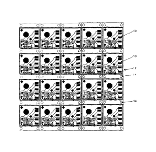
Step 1: PCB Printing
Printed Circuit Boards (PCB's) 10 are printed on a sheet 12 of suitable
flexible
substrate in 5-inch x 4-inch format. Figure 1.1 shows a sheet of such PCB's.
The holes 14 positioned around the periphery of each PCB are used to align the
PCB in an automatic soldering machine used to install electronic components on
the
PCB.
Step 2: Soldering Components on the PCB
Electronic components are installed on the PCB 10 using an automated soldering
machine. The sheet 12 of PCB's (Figure 1.1) is placed on the soldering
machine's
customized jig. The jig has protrusions on its surface that engage the holes
14 and thus
permit the sheet of PCB's to be located precisely therein. Once the sheet is
in place, the
components are soldered to the PCB. Figure 2.1 shows components positioned on
a
PCB. The components may include a capacitors 16, 18 an oscillator 20, a
resistor 22, a
diode, 24 and a microcontroller 26.
4
CA 02493410 2012-05-11
Step 3: Transferring Firmware to the PCB's
Firmware is software specifically designed to control microcontroller
operations.
Firmware is saved in individual files and uploaded to a particular website.
Each file
contains a Tag Firmware Version and a unique Tag Identification (ID) Number.
These
files are downloaded to a Personal Computer (PC) connected to a Wouter Box 28.
The Wouter Box 28 is a specialized piece of hardware that allows 20 PCB's to
be
programmed and serialized simultaneously. Figure 3.1 shows a Wouter Box 28.
The Wouter Box 28 is connected to a Nail Bed 30 comprising 100 pins to allow
the 20
PCB's carried by a sheet 12 to be programmed simultaneously. The Nail Bed 30
enables simultaneous transfer of 20 firmware files from a Wouter Box 28 to 20
PCBs. A
Nail Bed is shown in Figure 3.2 which schematically illustrates the process of
transferring
firmware from a PC to a Wouter Box to a Nail Bed to 20 MedicTM ECM Tags.
To control the transfer of firmware, "Big Burner", also known as QA1 software,
is
used. Big Burner software is installed on a PC connected to Wouter Box 28.
Figure 3.3
shows the screenshot of Big Burner software.
In addition to transferring firmware, Big Burner also verifies that the
oscillator
calibration coefficient is not corrupted due to poor contact between the Nail
Bed pins and
the PCB's. Big Burner automatically marks any PCB's that were not successfully
programmed with the firmware, so that these tags can be removed from the
assembly
process. Figure 3.4 shows a screenshot of Big Burner displaying a failed
attempt at
programming one of 20 PCBs. The failed attempt is shown with a large "X" at
position
number 4 in the bottom line of PCB's.
Step 4: Battery Installation on the PCBs
Once the PCB's are programmed, a 3.3-volt battery 32 is installed on each PCB
by soldering. Figure 4.1 shows a PCB with the battery installed thereon.
Step 5: Protective Foam Placement on the PCBs
A layer 34 of protective foam is applied to the PCB's. Since both sides of the
foam are adhesive, the foam is adhered to the PCB's. The front side of the
foam
identifies the PCB type (i.e., Med-icTM) and the Firmware Version. The
backside of the
foam has a protective paper layer attached. When adhering the foam 34 to the
PCB's,
this paper is first peeled off to expose the adhesive. The backside of the
foam is then
CA 02493410 2012-05-11
attached to the PCB's. Figure 5.1A and B show the front of the foam and a
single PCB
with foam attached.
Step 6: Foam Placement on the PCBs
Another layer 36 adhesive foam is glued to the back of the PCB's. This allows
the option of attaching PCB's to any paper material. Paper from one side of
the foam 36
is peeled off and that side is attached to the back of the PCB. The other side
of the
foam is left with its protective backing in place. When the PCB is to be
affixed onto a
paper material the protective backing is removed and the PCB attached. Figures
6.1
shows the front and back of the foam.
Step 7: PCB Sheet Separation
A sheet 12 of PCB's 10 is cut into 20 separate PCB's. These PCB's 10 are now
known as Tags, and will continue to be identified by the reference number 10.
Figure
7.1 shows the individual tags 10 separated from each other.
Battery Life Measurement:
To assure the quality of the batteries attached to the Tags, battery life is
now
measured.
The rate of loss of energy from batteries is often irregular, making it
difficult to
measure and predict. Factors such as quality, lithium content, connections of
anode and
cathode, and condition of the separator and electrolyte system can contribute
to
inconsistency in energy depletion.
Special firmware, "Battery Test Firmware", has been developed to monitor the
energy and voltage level of a battery through its entire life. Battery Test
Firmware
checks and records the energy and voltage level of a battery at regular
intervals.
Recorded information is displayed when the Tag is scanned on an RF reader
connected
to a PC loaded with the Battery Test Firmware..
Tags are randomly chosen from a production batch after they have been
completely assembled. These selected Tags are then programmed with the Battery
Test
Firmware using Big Burner software. A resistor of low tolerance (approximately
0.1%) is
connected to each programmed Tag. This resistor serves as a reference unit for
the
battery voltage measurements. These Tags are stored in a warehouse where they
are
6
CA 02493410 2012-05-11
periodically scanned to view the battery's energy and voltage level history.
The
functional life of a lithium battery is approximately 2 years.
Step 8: Quality Assurance Check on each Tag
Each Tag 10 is checked with Quality Assurance 2 (QA2) software. To
communicate with the Tag, QA2 software uses the CertiScan TM Reader 38. A Tag
10 is
placed on the reader to start communication with the QA2 software. The
procedure of
placing the Tag on a reader is also referred to as scanning. Figure
8.1 shows the
Certiscan TM Reader 38 and a Tag 10 being scanned.
QA2 checks Timer 1 and battery voltage. Any Tag that fails either of these
tests
is deemed unacceptable for further use. Tags that pass these checks are
assigned
unique ID Numbers that are saved to a QA2 floppy disc. In addition, the test
results for
each Tag are also saved. On completion of this step only successfully
programmed and
readable tags have passed through the inspection process. Figure
8.2 shows
screenshots of QA2 software.
Step 9: Shipping and Handling
Tags 10 that pass QA2 are placed in a plastic tray 40. A tray 40 is capable of
holding 80 Tags and 20 trays form a Lot. (Thus,1 Lot consists of 1600 Tags).
Each Lot
also includes a floppy disc 42 containing the ID numbers and QA2 test results
for all
Tags in that Lot. Three Lots are placed in one Box.
One percent of the Tags are held back for quality testing and are sent to the
engineering office. Boxes of tags are shipped to the user.
Figure 9.1 shows a tray 40 containing 80 Tags and the floppy disc 42 for the
Lot
to which this Tray belongs.
Description of Steps Involved in Producing a Printed Sensor Grid (PSG)
Compatible with a Med-ic TM ECM Tag
Having manufactured a large number of tags 10 for the blister package market,
it
is then necessary to marry each tag to a Printed Sensor Grid (PSG) adapted for
each
blister package provided with a tag. A PSG will carry the conductive
rupturable traces in
a particular pattern dependent on the layout of the blister package itself and
it will also
carry conductive stitching connecting the rupturable traces with the tag 10.
7
CA 02493410 2012-05-11
Background Information
A paper production facility designs and manufactures paper or paper label
stock
to work with Med-ic TM ECM Tags. A PSG is then printed on its surface. The PSG
is also
known as a Grid 44.
A Grid consists of conductive and resistive paths connected to a Tag 10 by
stitching with conductive thread, also the subject of separate patent
applications. This
puts the Tag 10 and Grid 44 in electrical continuity. Details of connecting a
Tag to a Grid
are described in Step 12 hereinafter. The connection between the Grid and the
Tag
enables the Tag to monitor the electrical characteristics of the Grid. The
electrical circuit
comprised of a connected Tag and Grid is shown in Figure B1 .
Operations of the Circuit
In Figure B1, components residing on the Tag 10 and the Grid 44 are enclosed
in
rectangles labelled "Tag" and "Grid". Power is supplied to this circuit by a
3.3 Volt
battery (Vdd).
Initially, Switch 1 is closed to allow Vdd to charge the Capacitor. The
Limiting
Resistor prevents overflow of current to the Capacitor. When the Capacitor is
charged to
approximately 1.1Volt, the Comparator records a Value of 1. This indicates
that the
Capacitor's charged value is higher than the Comparator's threshold value.
Figure B2
shows the operation of charging a Capacitor.
When the Comparator records a Value of 1, a Timer is set to zero. The
Capacitor is discharged to Ground through the components of the Grid. Closing
Switch
2 allows the Capacitor to discharge to Ground. Current flows first from the
Capacitor to a
Reference Resistor on the Grid. When the current reaches the point of the
Resistors in
parallel (Figure B1 with R2 in parallel with G_Switch 2), it chooses the path
of least
resistance and passes through the closed G_Switch. After passing through all
closed
G_Switches, the current goes through closed G_Switch 2 to ground. Figure B3
shows
the path taken by the current discharged from the Capacitor.
A Diode in the circuit prevents the current from flowing through the Limiting
Resistor. Therefore current is forced to take the path shown in figure B3. The
Reference Resistor is three times bigger than any other Resistor in the grid
circuit.
Since the printing of a grid can vary from grid to grid, the Resistors can
also vary. The
Reference Resistor provides an average value for a specific Tag to establish a
relative
current when the Capacitor is discharging.
8
CA 02493410 2012-05-11
As soon as the Capacitor begins discharging, a Timer is started to measure the
time it takes for the Capacitor to discharge. Once the Capacitor's discharge
value
reaches the Comparator's threshold value of 1.1 Volts, the Comparator records
a Value
of 0 and stops the Timer. The time measured by the Timer is stored in the
EPROM of
the microcontroller.
If G_Switch 2 in the grid is opened, as shown in Figure B4, the current's path
changes. Current now flows through R2, the path of least resistance. The path
through
R2 increases the time for the Capacitor to reach the threshold value of the
Comparator.
The Microcontroller compares the opening and closing times of G_Switch 2. If
the times do not match, the Microcontroller decides that G_Switch 2 is open.
Step 10: Printing Sensor Grids
Electronic components such as resistors and conductive traces are printed on
the
surface of the paper or label stock. Silver ink is used to print conductive
traces 46 and
carbon ink is used to print resistors 48 (resistive paths). These printed
elements are
collectively referred to as the Grid.
A Tag and Grid form an electronic circuit that allows the Tag to monitor the
Grid
for changes in its electrical characteristics. Figure B1 shows schematically
the circuit
formed by the Tag and the Grid. The Grid is printed on paper or label stock as
shown in
Figure 10.1. This Grid behaves and operates as described under the Background
section.
A Flexographic printing process as described in other patent applications is
used
to print the Grids. Figure 10.2 illustrates the step-by-step application of
coatings and
inks to the paper's surface. In lieu of or in addition to coating, protective
self-adhered
tape may be used.
As described in Figure 10.2, Step 1 involves choosing the paper thickness. Ten-
or 12-point paper is generally used. Alternatively, 3 mil or similar self-
adhesive label
stock may be used.
In Step 2 a layer of Curable Ultraviolet (UV) Coating is applied to the paper.
This
coating prevents cracks from forming in the resistive or conductive paths when
the paper
is bent. Cracks can interfere with the electrical continuity of the paths
causing the
system to malfunction.
In addition, paper is composed of fibres, making its surface irregular and
sensitive to changes in temperature and humidity. Changes in a paper's surface
9
CA 02493410 2012-05-11
architecture alter the electrical characteristics of paths printed on it.
Curable UV Coating
makes the paper's surface more uniform and resistant to temperature and
humidity
effects.
UV Coating also provides extra flexibility if the paper has a clay coating.
Clay
coating is applied to paper to make it glossy. The clay coating is brittle and
can crack
when the paper is bent. Consequently, Carbon or silver ink paths applied
directly to the
clay coat could lose their electrical continuity. Application of Curable UV
Coating to the
clay coat prevents this. In Step 3, Resistors and Traces are printed with
carbon or silver
ink.
Step 4 involves applying another layer of Curable UV coating. This layer is
applied on top of both carbon and silver inks and serves as an insulator to
prevent
electrical contact with outside sources other than the Tag. This coat also
fills in the
pores of the carbon and silver ink, serving as a bonding material. Self-
adhesive paper or
plastic tape can be used in conjunction with or in place of the coating. The
Grid shown
in Figure 10.1 is obtained on completion of the four steps in Figure 10.2.
Paper is not the only material on which the Grid can be printed. Paper label
stock, polymer film and paper-backed foil can also be used.
A layer of adhesive is applied to the bottom surface of the paper, as shown in
Figure 10.3.
When the paper is heated, this adhesive melts and attaches the paper to other
surfaces with which it is in contact. This process is explained in Step 15
hereinbelow.
The paper with its printed Grid is then die cut. Figure 10.4 shows a die cut
paper.
Referring back to Figure B4, G_Switch 2 is opened intentionally to change the
current's path. To open a switch on a Grid (see Figure 10.1) a section of the
conductive
path must be broken completely. A person needs to apply pressure on a specific
section
of the Grid to break that section. This action is taken when a blister package
of
medication is placed inside the paper with the plastic blisters protruding
through the die
cut holes in the paper, and the paper is heat sealed to enclose the blister
package. This
process is described in Step 14.
The Grid is aligned with the individual blisters in such a way that pushing a
tablet
through the backing of the blister package will break the associated path of
the Grid.
This forces the current to take a resistive path. However, breakage of the
conductive
path may occur in other sections of the Grid if pressure is not applied
properly. To
facilitate breaking in the appropriate area of the Grid, die cutting is used
to score
CA 02493410 2012-05-11
patterns, as at 50, around areas of the Grid that are required to serve as
switches.
Figure 10.4 shows a Die Cut Grid.
When a tablet is expelled from its blister, it breaks the path in the section
of the
Grid at the associated scored area. A semi-circular pattern of scores 50
prevents
creases from forming on conductive paths when heat-sealed paper with an
enclosed
blister package is deformed. Creases cause resistance changes in the
conductive
paths, resulting in malfunction of the system. Figure 10.5 shows a broken path
with its
associated score pattern.
The scoring pattern acts like a door, allowing the tablet to break the grid
and slide
out.
Step 11: Checking Grid Resistances
Once the paper Grid has been die cut, a unique ID Number is assigned to it.
The
Grid's resistances must then be verified. Grid resistances must fall into a
range for that
Grid to be acceptable.
The generation of an ID Number and verification of the Grid's resistances is
done
by proprietary software known as "Package Quality Assurance One" (PQA1)
Software.
PQA1 is installed on a PC with a Label Maker and a Multimeter connected to the
PC.
When launched, PQA1 automatically detects if the Label Maker and Multimeter
are
connected and operating. It also checks that a specific database and
connection to it
exist. This database contains all the ID Numbers for various types of paper
substrate.
Once PQA1 has verified that the peripherals and database are connected, it
allows a
user to enter the type of paper being checked. When the <Print> button is
pressed,
PQA1 retrieves a unique ID Number for that type of paper and generates a
label, using
Label Maker, with that number printed on it. This label also contains a
barcode
representing the ID Number. Figure 11.1 shows a screenshot of a paper type
entered
into PQA1 software.
The Label is pasted on the paper adjacent to the Grid and shows the ID Number
of that paper Grid. PQA1 completes Step 1 and progresses to Step 2, where it
displays
the unique ID Number and enables a user to measure the Grid's resistances.
A Grid preferably consists of two smaller grids 52, 54. The reason for
dividing
the Grid into sub-grids is that if one grid fails the other is not affected
and the overall Grid
would still operate. It also reduces the overall magnitude of resistance by
half.
11
CA 02493410 2012-05-11
=
The resistances are measured using a Multimeter with its probes first placed
on
common and Grid 1 (52), and then on common and Grid 2 (54). Resistances are
read
automatically by the Multimeter and transmitted to PQA1 software. Figure 11.2
shows a
Grid and identifies the sub-grids and areas where the probes are placed.
PQA1 software accepts the measured resistances and checks to see whether
these resistances fall into an acceptable range. If a resistance is outside
the range
PQA1 highlights that resistor's field in colour red. Figure 11.3 shows a
screenshot of
PQA1 software with both steps completed.
When the <Submit> button is pressed, PQA1 records the resistances measured
to a database with reference to that particular Grid ID Number.
Further Quality Assurance (QA) is conducted on 32-Dose and 18-Dose Grids by
measuring each printed resistor. Figure 11.4 shows a 32-Dose Grid with silver
ink pads
56 printed on it to enable measurement of each resistor (black, carbon ink
path).
The contact pad 56 divides each resistor into two parallel resistors. The
resistance of an individual resistor can be determined by placing the two
probes of a
Multimeter on the adjacent contact pads. This procedure allows non-destructive
testing
of the Grid. A Nail Bed can be used to automate the procedure. Some conductive
inks
dry more slowly than others and during this process their conductivity will
change. With
such inks it is desirable to perform repeated resistance measurements during
the first 3
to 4 weeks after printing, until stable resistances occur. For even slower
drying inks it
may be desirable to use such measurements to predict the ultimate resistances
that will
occur during the grid's useful life.
Each resistor value R obtained during such measurement is compared to the
minimal allowable value, calculated as:
Rmm > (Rref/3) ¨ 5%
Failure to compare the individual resistors to the grid's reference resistor
can
introduce multiple undetected expulsion events. Making such comparisons at
several
points during the curing process will detect abnormal ink curing due to
inconsistencies in
the grid substrate.
When paper with a grid printed on it is bent the resistance of the grid
changes.
Such changes in resistance could cause the attached tag to record incorrect
events.
(The attachment method is described in Step 12). To address this problem, a
second,
mirror grid is printed on the obverse of the paper. Grids printed on both
sides of the
paper substrate provide a stable resistance value to the tag when the grid is
bent.
12
CA 02493410 2012-05-11
Explanation of Resistance Variation:
Total resistance is based on the length of the resistor and the resistance per
square unit of printed resistor. Equation E11.1 shows the relationship:
RTotal = Length * (Re/square)(E11.1)
A resistor printed on paper is shown in cross-section in Figure 11.5. The
total
resistance of this resistor (R1) is equivalent to its length (L1) multiplied
by the resistance
per square unit.
If the paper is bent convexly, as shown in Figure 11.6, the total resistance
(R1) of
the Resistor will change since the length of the resistor increases. The new
resistance
R2 is greater than R1.
Conversely, if the grid is bent concavely the resistor's length is decreased
and
total resistance R3 will be less than R1. This is illustrated in Figure 11.7.
If a mirror grid is printed on the back of the paper substrate, bending will
cause
R2 to increase on one side and R3 to decrease on the other, giving the
expected
resistance R1. The two grids on opposite sides of the paper must both be in
electrical
continuity with the tag as illustrated in Figure 11.8. The equivalent circuit
created by this
method is shown in Figure 11.9.
Step 12: Stitching Paper with a Tag
Grids passing QA and having unique ID Numbers attached progress to a
stitching station. Here, a BrotherTM BAS-311F-0 Automated Stitching Machine 57
(Figure 12.1) attaches the tag to the appropriate points of the printed grid
using silver
conductive thread. Figure 12.2 shows a tag 10 stitched to a grid 44 via
conductive
stitching 58.
Each stitching procedure is inspected visually and any loose conductive fibers
are removed and a protective self-adhesive label is applied.
A tag stitched to a grid records the time of any significant resistance change
in
the grid. The applicant implements a unique method to calculate precise time,
as
discussed below.
13
CA 02493410 2012-05-11
Calculation of Time by the Tag
Time calculated by the PC is assumed to be accurate as it is synchronized with
an Atomic Clock. The PC's clock is updated at interval T1 of every second.
After 60
intervals, the PC updates the minute counter. The tag 10 uses an oscillator 20
containing a crystal resonator to calculate time. The oscillator updates the
tag's clock
every interval T2. In general, the accuracy of the time calculated by the
oscillator is
determined by the quality of the crystal resonator. T2 is 1 second plus or
minus delta A.
Delta A is the error introduced by the crystal resonator. Figure 12.3 shows
the PC's
accurate time interval T1 of one second and the oscillator's time interval T2.
Equation E12.1 shows the relationship between T1 and T2.
T1 = T2 delta A (E12.1)
If the crystal resonator is of good quality, delta A, will be small. However,
accurate crystal resonators are expensive, as they require time to calibrate
to the correct
frequency.
To reduce delta A, a method that uses the firmware on the reader to calculate
the
precise time recorded by the tag has been developed. This method adjusts the
interval
T2 of the oscillator so the counter incremented at T2 coincides with the CPU
clock
counter change. When a tag is scanned on a reader, the reader records the time
on its
clock and the tag's counter value and notes them as Tsyncl and 1\110c.a11,
respectively.
When the tag is scanned again, the reader again records its clock time and
stores the
counter value of the tag. These values are noted as Tsync2 and N0cal2.
The reader applies equation E12.2 to calculate the T2 value by which the tag's
oscillator should be adjusted.
T2new = (Tsync2 Tsyncl)I (N10ca12 Nlocall)
(E12.2)
The reader uses T2new and equation E12.3 to adjust all the times recorded by
the
tag. Individual event times recorded by the tag are denoted as Tevent=
Tevent = Tsyncl + (tag's counter) * T2new (E12.3)
14
CA 02493410 2012-05-11
Step 13: Checking the Connection between the Tag and the Grid
A stitched tag and grid forms an electronic circuit as shown in Figure 81. To
verify that this circuit has been created the connection between the tag and
the grid must
be verified. The tag's internal components such as the timer must also be
tested.
Proprietary "Package Quality Assurance 2" (PQA2) software does these tests.
PQA2 requires a barcode scanner, CertscanTM reader, and digital camera to be
connected to the PC on which is installed PQA2. PQA2 is launched and a
stitched grid
and tag unit is placed on the Certiscan TM reader. While on the reader the
barcode label
attached to the grid's substrate is scanned by the barcode scanner. PQA2
receives the
scanned result, which is the ID Number of that grid, and checks with the
database to
confirm it is a valid ID Number. If the check fails, PQA2 notifies the
operator of the
problem and requests the next grid and tag unit for scanning. If the ID Number
is valid,
PQA2 sets the tag's ID Number to match the grid's ID Number. It also tests the
tag's
microcontroller timer, instructs tag to measure the grid resistances, and
compares these
measured resistances with a predefined resistance range and with the
resistances
determined by PQA1.
If all operations are successful, PQA2 judges this grid and tag assembly
acceptable for use and displays "PASS" on its screen. Figure 13.1 shows a
screenshot
of a stitched paper judged as "PASS" by PQA2. If any of the operations fail,
PQA2
prohibits the user from using that grid and tag unit and displays "FAIL" on
its screen.
Regardless of Pass or Fail status, a digital image of the grid and tag unit is
taken
automatically by PQA2 for future reference. PQA2 then permits the user to save
all the
results of its operations by pressing <Submit>. Once <Submit> is pressed, PQA2
saves
all its results to the database with reference to the grid and tag unit ID
Number. Figure
13.2 shows a PQA2 workstation with the peripherals attached to the PC and PQA2
software operating.
Step 14: Inserting the Blister Package into the Stitched Paper
A blister package containing medication is inserted into a stitched grid and
tag
unit. The type of paper used depends on the type of blister package being
inserted.
Figure 14.1 shows the front and back of a 14-Dose blister package.
A 14-Dose paper grid is required to accommodate a 14-Dose blister package.
The paper grid 60 has cut outs with precise dimensions and locations that
allow a blister
CA 02493410 2012-05-11
package to be inserted. Figure 14.2 shows a 14-Dose paper with and without a
blister
package inserted.
The paper substrate is folded to create a package containing the grid,
attached
tag, and blister package. Figure 14.3 shows and describes the steps to fold
the paper
substrate. The
end result is a compact package containing all essential elements,
namely the blister package with its pills, capsules or other medication held
within
individual blisters, and the grid adhered to the back of the blister package
so that a
conductive trace is ruptured when the contents of a blister are expelled
therefrom,
allowing the tag to record the time and any other relevant information.
Step 15: Heat-Sealing
The folded paper in Step 5 of Figure 14.3 contains a blister package and
stitched
tag. The folded paper is now heat-sealed to create a functional package. The
folded
paper is placed in a heat-seal machine 62 at 320 Fahrenheit for 7 seconds.
Figure 15.1
shows a view of the heat-seal machine 62.
The temperature of Heat-Seal machine is set by a dial on the machine. A
temperature gauge indicates the current temperature. A lever closes the top
over the
bottom.
The foregoing has described the steps involved in the production of a MedicTM
ECM tag. It is also understood that the present method could be applied to
other
products of a similar nature. The scope of the claims should not be limited by
the
preferred embodiments set forth in the examples, but should be given the
broadest
interpretation consistent with the description as a whole.
16