Note: Descriptions are shown in the official language in which they were submitted.
CA 02493942 2005-O1-26
WO 2004/015870 PCT/CA2003/001204
METHOD AND DEVICE FOR INJECTION LOCKING OF VOLTAGE CONTROLLED OSCILLATORS
USING DIRECT DIGITAL TUNING
BACKGROUND TO THE INVENTION
**Cop~iricrht Notice**
A portion of the disclosure of this patent document contains material which is
subject fo copyright protection. The copyright owner has no objection to the
facsimile reproduction by anyone of the patent document or the patent
disclosure, as it appears in the Patent and Trademark Office patent file or
records, buf otherwise reserves all copyright rights whatsoever
1o Field of Invention
The invention relates to the field of electronics and more particularly to the
tuning and injection locking of voltage controlled oscillators (VCOs).
Description of the Related Prior Art
As will be understood by those skilled in the art, an oscillator is an
electronic device used for the purpose of generating a signal. Oscillators are
found in computers, audio-frequencyequipment, particularly music synthesizers,
2o and wireless receivers and transmitters. There are many types of oscillator
devices, but they all operate according to the same basic principle: an
oscillator
always employs a sensitive amplifier whose output is fed back to the input in
phase. Thus, the signal regenerates and sustains ifiself. This is known as
positive
feedback.
As will be also understood by those skilled in the art, some oscillators
employ combinations of inductors, resistors, andlor capacitors to generate
their
operating frequency such as resistor-capacitor (RC) and inductor-capacitor
(LC)
1
CA 02493942 2005-O1-26
WO 2004/015870 PCT/CA2003/001204
oscillators. However, the best stability (constancy of frequency) is obtained
in
oscillators that use quartz crystals. When a direct current is applied to such
a
crystal, it vibrates at a frequency that depends on its thickness, and on the
manner in which it is cut from the original mineral rock.
A voltage-controlled oscillator (VCO) is a circuit that generates an
oscillating signal at a frequency proportional to an externally applied
voltage.
VCOs are often found in phase-locked loops (PLLs) used for, among other
things, synchronizing an oscillation frequency to an external reference, or to
a
higher multiple or derivative of a crystal reference. In the first case
(called clock
recovery) the goal is to recreate a clock signal synchronous to that which was
used to generate a data stream. In the second case, the goal is to generate a
higher frequency signal that has the phase noise properties of a low frequency
reference. The phase noise of a VCO is generally very poor and does not meet
the need of many applications. It is also unpredictable in terms of it's
nominal
frequency and drift. The crystal on the other hand is much more exact and has
better phase noise. To generate a high radio frequency (RF) using a lower
frequency crystal oscillator as a reference, a PLL is used.
2o Figure 1 depicts a block diagram of a frequency tuning circuit including a
PLL with VCO circuit. The circuit consists of an oscillator 20 or external
reference clock, a phase detector 22, a low-pass filter 24, a gain stage 26, a
VCO 28 and a divider 29 configured in a loop. The phase detector is a circuit
that normally has an output voltage with an average value proportional to the
phase difference between the input signal from oscillator 20 and the output of
VCO 28. The low-pass filter 24 is used to extract the average value from the
output of the phase detector 22. The average value is then amplified and used
to drive the VCO 28. The divider 29 transforms the high frequency Vosc into a
low frequency V'osc. The negative feedback of the loop results in the output
of
3o the VCO 28 being synchronized or locked with the input signal from
oscillator 20.
In this locked condition, any slight change in the input signal first appears
as a
change in phase between the input signal and the VCO frequency. The phase
2
CA 02493942 2005-O1-26
WO 2004/015870 PCT/CA2003/001204
shift then acts as an error signal to change the VCO frequency to match the
input signal. In other words, the purpose of the phase detector 12 is to
produce
and output which represents how far the frequency produced in VCO 18 is from
that of the input signal. Comparing these frequencies and producing an error
signal proportional to their difference allows the VCO frequency to shift and
become the same frequency as the input signal.
An alternate to PLL is injection locking which does not require the design
of a high frequency phase detector or divider circuitry. The process of
injection
locking is a fundamental property of oscillators, in that it can be observed
in a
wide variety of oscillator types with the same qualitative behaviour observed
in
each case. When a periodic signal is injected into an oscillator (e.g. a VCO)
with
a free-running frequency fo, by summing it with the state oscillation signal,
the
oscillator will lock to and track the injected signal frequency over fo +/-
LBW/2,
~5 where LBW is the locking bandwidth. Within this lock range, the process can
be
modeled as a true first-order PLL which implies that the loop is
unconditionally
stable and that the phase noise of the output tracks the phase noise of the
injected clock over a wide bandwidth. Moreover, the locking bandwidth (LBW)
increases forlarger injection amplitudes. For example, to accommodate process
2o and environment variations, typical radio frequency (RF) applications
require an
LBW of 25 - 50 M Hz greater than the signal bandwidth. However, achieving this
LBW typically requires a large injection signal power, which is undesirable in
certain applications such as integrated (as opposed to discrete) circuits.
Further,
given the inherent advantages of digital (as opposed to analogue) signal
25 processing, the ability to determine the oscillation frequency of the VCO
using
a digital circuit v~ould be advantageous. In particular, in an integrated
circuit
environment, the ability to eliminate off-chip components and to reduce the
overall chip area is desirable.
3o SUMMARY OF THE INVENTION
3
CA 02493942 2005-O1-26
WO 2004/015870 PCT/CA2003/001204
In order to overcome the deficiencies of the prior art, an improved
injection locking circuit is provided which allows the VCO to injection lock
with a
smaller LBW and associated lower signal power. By ensuring that the free
running oscillator frequency is close to the injection harmonic, independent
of
process and environmental variation, the required LBW is greatly reduced. As
a result, the injection power and associated power dissipation is also
reduced.
Further, the signal processing capabilities of digital circuits is used to
determine
the oscillation frequency of the VCO without requiring extensive additional
circuitry.
In order to allow the VCO to injection lock with a smaller reference signal
and therefore a smaller LBW, this invention includes a pre-tuning algorithm to
place the VCO frequency such that the desired frequency is in the desired LBW.
Tuning of the VCO is achieved using direct digital tuning that does not
require
an input reference. Injection locking is performed using a low frequency clock
harmonic as the reference signal. The output signal of the VCO is sub-sampled
and digitized, the center frequency determined and the VCO control voltage
adjusted. The VCO output can be further sub-sampled and digitally tuned so
that it is within the LBW of a reference signal.
In accordance with one aspect of the invention there is provided a method
of digitally pre-tuning and injection locking a voltage controlled oscillator
(VCO)
comprising the steps of: digitally pre-tuning the VCO to within a specified
locking
bandwidth (LBW); injecting an input reference signal into said VCO; and
locking
said VCO to said input reference signal.
Preferably, the step of digitally pre-tuning comprises the steps of:
digitizing the VCO output; determining the VCO output frequency; adjusting the
VCO output frequency; and repeating the steps of digitizing, determining and
3o adjusting until a desired oscillation frequency is reached.
4
CA 02493942 2005-O1-26
WO 2004/015870 PCT/CA2003/001204
In accordance with a second aspect of the invention a circuit for digitally
pre-tuning and injection locking a voltage controlled oscillator (VCO)
comprising:
a reference oscillator for producing a reference input signal; a VCO
electrically
connected to said reference oscillator; and a feedback circuit electrically
connected to said VCO for digitally pre-tuning said VCO and receiving a
reference.
Preferably, the feedback circuit comprises an analogue-to-digital (ADC),
microcontroller and a digital-to-analogue converter (DAC), wherein a control
1o signal is produced in the microcontroller and injected into the VCO.
20
The advantage of the present invention is now readily apparent. A low
power oscillator incorporating injection locking with direct digital tuning is
provided with improved locking range.
BRIEF DESCRIPTION OF THE DRAWINGS
A better understanding of the invention will be obtained by considering the
detailed description below, with reference to the following drawings in which:
Figure 1 depicts a block diagram of an oscillator circuit including a PLL
with VCO circuit in accordance with the prior art;
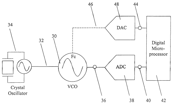
Figure 2 depicts a block diagram of the VCO tuning and injection locking
system in accordance with the present invention;
Figure 3 depicts an example VCO circuit with injection input port in
accordance with the present invention; and
3o Figure 4 a flow diagram of the tuning and injection locking process in
accordance with the present invention.
5
CA 02493942 2005-O1-26
WO 2004/015870 PCT/CA2003/001204
DESCRIPTION OF THE PREFERRED EMBODIMENT
The invention may be embodied in many different forms and should not
be construed as limited to the embodiments set forth herein; rather, these
embodiments are provided so that this disclosure will be thorough and
complete,
and will fully convey the scope of the invention to those skilled in the art.
In the
drawings, like numbers refer to like elements throughout. The accompanying
drawings and the description below refer to the preferred embod invent, but is
not
limited thereto.
The present invention arises from the realization that the signal
processing capabilities of digital circuits, such as those commonly employed
in
radio transceiver circuits, may be used to determine the oscillation frequency
of
a VCO without requiring extensive additional circuitry.
As shown in Figure 2, the tuning of the VCO 30 is accomplished in the
digital domain and involves three main components: analogue-to-digital
converter (ADC) 38, digital microcontroller 42 and digital-to-analogue (DAC)
converter. To begin, reference signal 32 normally inputted to VCO 30 from the
2o reference crystal oscillator 34 is turned off. Pre-tuning is performed by
first sub-
sampling VCO output 36 is first sub-sampled by ADC 38. The sub-sampled
signal 40 is then processed in the digital domain using digital m
icrocontroller 42
where the center frequency (f~) of the VCO 30 is determined. As a skilled
workman will appreciate, several methods are available for determining f~. For
example, f~ can be determined by performing a Fast Fourier Transformation
(FFT) of the sampled data, removing the narrow band desired signal and any
other interfering signals, smoothing the amplified noise if necessary and
finding
the peak of the resultant frequency response. A more efficient approach is to
replace the FFT with a digital down-conversion stage. The resulting phase
shift
so from one sample to the next can be measured to calculate the frequency, f~
of
the VCO 30. Once the VCO frequency is determined it is adjusted by generating
digital control signals 44 that are converted to analog signals 46 using DAC
48.
6
CA 02493942 2005-O1-26
WO 2004/015870 PCT/CA2003/001204
This feedback process involving the ADC 38, microprocessor 42 and DAC 48 is
continuously repeated until the desired VCO frequency is reached.
By pre-tuning VCO 30 so that its oscillation frequency f~ is close to the
s desired frequency, the required LBW is reduced significantly. A reduction in
the
LBW reduces the required power of reference signal 32. This allows a lower
frequency reference signal with significant higher harmonics to be used as the
reference signal. In the preferred embodiment, a low frequency crystal
oscillator
is used to injection lock an RF VCO with the Nt" harmonic, where N is the
result
of dividing the VCO frequency with the fundamental crystal frequency.
Once the VCO 30 is tuned within the LBW, the input to the VCO 30 is
turned on, allowing the reference signal 32 to be injected into VCO 30. In the
preferred embodiment, the reference signal 32 takes the form of a crystal
oscillator 34 whose high frequency harmonics contain one such harmonic at the
desired oscillation frequency for the VCO. The VCO is tuned close enough to
th is desired oscillation frequency to allow injection locking. Once the
reference
signal is applied, the VCO remains locked to the harmonic of the crystal
oscillator.
Figure 3 depicts a sample circuit diagram used in the preferred
embodiment of VCO 30. The tank circuit of the VCO is comprised of inductors
48 and variable capacitors 50. As will be appreciated by those in the art, a
tank
circuit is a parallel resonator circuit comprised of an inductor, a capacitor
and an
2s optional resistor. Since the capacitor and the inductor both store energy,
it is
commonly referred to as a tank circuit. As will also be appreciated, variable
capacitors 50 could be replaced with a set of switched capacitor banks.
Returning to Figure 3, the variable capacitors 50 have a control voltage
so 52 that is adjusted by the digital-to-analog converter 48. The losses in
the tank
circuit are cancelled by the negative impedance created by a differential pair
of
transistors 54. This creates the condition for oscillation. The input
differential
7
CA 02493942 2005-O1-26
WO 2004/015870 PCT/CA2003/001204
pair of transistors 56 converts the input reference to a current. The current
is
injected into the tank circuit of the VCO 30 (i.e. added to the current signal
of
the oscillator tank circuit).
Figure 4 is a flow diagram of the tuning and injection process in operation.
When the VCO is initially powered up 100, the VCO oscillates 110 and the
output is sub-sampled 120. The oscillation frequency, f~ is determined 130 in
the
digital domain. Next, a test is performed 140 to see if f~ is within the
predetermined LBW range. If f~ is correct then the tuning cycle is complete,
the
input to the VCO is turned on 150 and the VCO is injection locked to the
reference signal 160. If f~ is not correct then the control signal is adjusted
170
and the tuning process is repeated.
The above description of the preferred embodiment utilizes direct
15 digitization of the VCO signal. As will be understood by those skilled in
the art,
sub-sampling of the VCO output is a good method for digitizing a narrow-band
high frequency signal but the step of digitizing could also be accomplished by
mixing down to an intermediate frequency (IF) and then digitizing with the ADC
by sampling or sub-sampling. This alternate embodiment is also meant to be
2o included within the scope of the invention.
In addition, the preferred embodiment uses digital circuitry to determine
the oscillation frequency of the VCO. The present invention is not limited to
this
embodiment. Other circuits can be construed that would be capable of
2s determining the oscillation frequency of the VCO using analog circuitry.
This
analog circuitry in turn could be used to adjust the frequency of the VCO
until it
is within the LBW of the desired signal and the injection locking is then
turned
on.
so Finally, the preferred embodiment uses a microcontroller for processing
the sub-sampled VCO output signal within the digital domain. As a workman
skilled in the art will appreciate, a microcontroller is usually embedded into
some
s
CA 02493942 2005-O1-26
WO 2004/015870 PCT/CA2003/001204
other device (e.g. a radio transceiver) and typically includes: (a) a central
processing unit (CPU) that executes software programs; (b) Random Access
Memory (RAM); (c) Erasable Programmable Read Only Memory (EPROM); (d)
serial and parallel I/O; (e) timers; and (f) an interrupt controller. In the
present
invention, the processing could be equally accomplished by the use of pure
digital circuitry designed to perform the functions described in relation to
Figure
2 (e.g. performing an FFT).
As will be understood by those skilled in the art, the present invention
relates to an injection locking circuit incorporating direct digital tuning.
The circuit
described herein can be produced in discrete or integrated circuit form and
may
be used in combination with other components to perform a specified analogue
or digital function in, for example, a radio transceiver. It is to be
understood by
the reader that a variety of other implementations may be devised by skilled
15 persons and the claimed invention herein is intended to encompass all such
alternative implementations, substitutions and equivalents. Persons skilled in
the field of electronic circuit design will be readily able to apply the
present
invention to an appropriate implementation for a given application. For
example,
other types of VCOs or tuning algorithms could be used.
A person understanding this invention may now conceive of alternative
structures and embodiments or variations of the above all of which are
intended
to fall within the scope of the invention as defined in the claims that
follow.
9