Note: Descriptions are shown in the official language in which they were submitted.
CA 02494487 2005-02-02
WO 2004/012896 PCT/US2003/023792
METHOD AND APPARATUS FOR HIGH VOLUME ASSEMBLY OF
RADIO FREQUENCY IDENTIFICATION TAGS
BACKGROUND OF THE INVENTION
Field of the Invention
The present invention relates generally to the assembly of electronic
devices. More particularly, the present invention relates to the assembly of
radio frequency identification (RFID) tags.
Related Art
Pick and place techniques are often used to assemble electronic
devices. Such techniques involve a manipulator, such as a robot arm, to
remove integrated circuit (IC) dies from a wafer and place them into a die
carrier. The dies are subsequently mounted onto a substrate with other
electronic components, such as antennas, capacitors, resistors, and inductors
to
form an electronic device.
Pick and place techniques involve complex robotic components and
control systems that handle only one die at a time. This has a drawback of '
limiting throughput volume. Furthermore, pick and place techniques have
limited placement accuracy, and have a minimum die size requirement.
One type of electronic device that may be assembled using pick and
place techniques is an RFID "tag." An RFID tag may be affixed to an item
whose presence is to be detected andlor monitored. The presence of an RFID
tag, and therefore the presence of the item to which the tag is affixed, may
be
checked and monitored by devices known as "readers."
As market demand ilzcreases for products such as RFID tags, and as
die sizes shrink, high assembly throughput rates for very small die, and Iow
production costs are crucial in providing commercially-viable products.
Accordingly, what is needed is a method and apparatus for high volume
CA 02494487 2005-02-02
WO 2004/012896 PCT/US2003/023792
assembly of electronic devices, such as RFID tags, that overcomes these
limitations.
SUMMARY OF THE INVENTION
The present invention is directed to methods, systems, and apparatuses
for producing one or more electronic devices, such as RFID tags, that each
include a die having one or more electrically conductive contact pads that
provide electrical connections to related electronics on a substrate.
In a first aspect, a plurality of RFID tags is assembled according to the
present invention. A plurality of dies are separated from a scribed wafer and
attached to a transfer or support surface (commonly referred to as a "green
tape" in the industry). The dies are transferred from the support surface to
corresponding tag substrates either directly or via one or more intermediate
surfaces.
In a first aspect, dies are transferred between surfaces using an
adhesive surface mechanism and process.
In another aspect, dies are transferred between surfaces using a
punching mechanism and process.
In another aspect, dies are transferred between surfaces using a multi-
barrel die collet mechanism and process.
In another aspect, a die frame is formed. Furthermore, dies are
transferred using the die frame.
In one aspect for making a die frame, a wafer that comprises a plurality
of dies is attached to a surface of a tape structure. A grid of grooves is
formed
in the wafer to separate the plurality of dies on the surface of the tape
structure. A portion of the tape structure that is accessible through the
grooves
of the grid is caused to harden into a grid shaped structure. The grid shaped
structure removably holds the plurality of dies. One or more dies of the
plurality of dies can be moved from the grid shaped structure onto a target
surface.
CA 02494487 2005-02-02
WO 2004/012896 PCT/US2003/023792
-3-
In another aspect for making a die frame, a wafer that comprises a
plurality of dies is attached to a surface of a tape structure. The tape
structure
comprises an encapsulated hardening material. A grid of grooves is formed in
the wafer to separate the plurality of dies on the surface of the tape
structure.
The surface of the tape structure is breached in the grooves while forming the
grooves to cause the encapsulated hardening material to harden in the grooves
into-a grid shaped hardened material in the grooves of the grid.
In an aspect, dies may be transferred from a die frame made according
to the present invention. A die ,frame is positioned closely adjacent to a
surface of a substrate such that a die of a plurality of dies removably held
in
the die frame is closely adjacent to the substrate. The die is transferred
onto
the closely adjacent substrate from the die frame. Each die may be transferred
from the die frame to the closely adjacent surface in this ma~u~er. Dies may
be
transferred from the die frame one by one, or multiple dies may be transferred
at a time.
Tn one aspect, dies may be transferred between surfaces in a "pads up"
orientation. When dies are transferred to a substrate in a "pads up"
orientation, related electronics can be printed or otherwise formed to couple
contact pads of the die to related electronics of the tag substrate.
In an alternative aspect, the dies may be transferred between surfaces
in a "pads down" orientation. When dies are transferred to a substrate in a
"pads down" orientation, related electronics can be pre-printed or otherwise
pre-deposited on the tag substrates.
In another aspect, a system for forming a die frame is described. A
wafer preparation module applies a wafer to a surface of a tape structure. The
wafer preparation module forms a grid of grooves in the wafer to separate the
plurality of dies on the surface of the tape structure. A hardening agent
source
causes a portion of the tape structure that is accessible through the grooves
of
the grid to harden into a grid shaped structure. The grid shaped stnzcture
removably holds the plurality of dies. One or more dies of the plurality of
dies
can be moved from the grid shaped structure onto a target surface.
CA 02494487 2005-02-02
WO 2004/012896 PCT/US2003/023792
-4-
In still another aspect, another system for forming a die frame is
described. A wafer preparation module applies a wafer to a surface of a tape
structure. The wafer preparation module forms a grid of grooves in the wafer
to separate the plurality of dies on the surface of the tape structure. The
tape
structure comprises an encapsulated hardening material. A wafer singulation
module forms a grid of grooves in the wafer to separate the plurality of dies
on
the surface of the tape structure. The wafer singulation module breaches the
surface of the tape structure in the grooves when forming the grooves to cause
the encapsulated hardening material to harden in the grooves into a grid
shaped hardened material
In another aspect of the present invention, a system and apparatus
enables the assembly of RFID tags. A die transfer module is present to
transfer a plurality of dies from the support surface to the tag substrates in
either a pads up or down manner
In another aspect of the present invention, an alternative system and
apparatus enables the assembly of RFID tags. A wafer preparation module is
present to transfer the dies from the support surface to a transfer surface. A
die transfer module transfers the dies from the transfer surface to the tag
substrates in either a pads up or down manner.
These and other advantages and features will become readily apparent
in view of the following detailed description of the invention.
BRIEF DESCRIPTION OF THE DRAW1NGS/FIGURES
The accompanying drawings, which are incorporated herein and form a
part of the specification, illustrate the present invention and, together with
the
description, further serve to explain the principles of the invention and to
enable a person skilled in the pertinent art to make and use the invention.
FIGS. lA shows a block diagram of an exemplary RFID tag, according
to an embodiment of the present invention.
FIGS. 1B and 1 C show detailed views of exemplary RFID tags,
according to embodiments of the present invention.
CA 02494487 2005-02-02
WO 2004/012896 PCT/US2003/023792
-5-
FIGS. 2A and 2B show plan and side views of an exemplary die,
respectively.
FIGS. 2C and 2D show portions of a substrate with a die attached
thereto, according to example embodiments of the present invention.
FIG. 3 is a flowchart illustrating a continuous-roll tag assembly
operation.
FIGS. 4A and 4B are plan and side views of a wafer having multiple
dies affixed to a support surface, respectively.
FIG. 5 is a view of a wafer having separated dies affixed to a support
surface.
FIG. 6 shows a flowchart providing steps for transferring dies from a
first surface to a second surface, according to embodiments of the present
invention.
FIG. 7 shows a flowchart providing steps for transferring a plurality of
dies from a first surface to a second surface using an adhesive surface.
FIGS. g-IO show views of a plurality of dies being transferred from a
first surface to a second surface using an adhesive according to the process
of
FIG. 7.
FIG. 11 is a flowchart illustrating a "pads up" die transfer onto a tag
substrate.
FIGS. 12A and 12B are plan and side views, respectively, of a plurality
of dies in contact with a support surface and a transfer surface.
FIG. 13 is a view of a plurality of dies attached to a transfer surface.
FIG. 14 is a view of a "pads up" oriented die in contact with a transfer
surface and a tag substrate.
FIG. 15 is a view of a "pads up" oriented die attached to a tag
substrate.
FIG. 16 is a flowchart illustrating a "pads down" die transfer onto a tag
substrate.
FIG. 17 is a view of a plurality of dies in contact with primary and
secondary transfer surfaces.
CA 02494487 2005-02-02
WO 2004/012896 PCT/US2003/023792
-6-
FIG. 18 is a view of a plurality of dies attached to a secondary transfer
surface.
FIG. 19 is a view of a "pads down" oriented die in contact with a
transfer surface and a tag substrate.
FIG. 20 is a view of a "pads down" oriented die attached to a tag
substrate.
FIG. 21 shows a flowchart providing steps for transferring a plurality
of dies from a first surface to a second surface using a parallel punching
process, according to embodiments of the present invention.
FIGS. 22-29 show views of a plurality of dies being transferred from a
first surface to a second surface using the punching process of FIG. 21.
FIG. 30 shows a flowchart providing steps for assembling RFC tags,
according to embodiments of the present invention.
FIGS. 31-36 show views of a plurality of dies being transferred from a
chip carrier to a substrate using the punching process of FIG. 30.
FIGS. 37-39 show view of substrate structures that include a plurality
of individual substrates.
FIGS. 40-45 show views of a plurality of dies being transferred from a
chip carrier to a substrate using the punching process of FIG. 30.
FIGS. 46 and 47 show views of the formation of electrical conductors
on a substrate.
FIGS. 48A and 48B show views of an example multi-barrel die
transfer apparatus, according to an embodiment of the present invention.
FIG. 49 shows a flowchart providing example steps for transfernng
dies using a multi-barrel die transfer apparatus, according to an embodiment
of
the present invention.
FIG. 50 shows a cross-sectional view of a mufti-barrel transfer
apparatus being applied to first surface.
FIGS. 51 and 52 show cross-sectional views of a mufti-barrel transfer
apparatus transferring dies to second surfaces.
CA 02494487 2005-02-02
WO 2004/012896 PCT/US2003/023792
_7_
FIG. 53 shows a cross-sectional top view of an example barrel with die
inside, according to an embodiment of the present invention.
FIG. 54 is a flowchart illustrating a post processing operation.
FIGS. 55 and 56 are block diagrams of tag assembly devices.
FIGS. 57A and 57B show flowcharts providing steps for making a die
frame, according to example embodiments of the present invention.
FIG. 58-62 show example views of a wafer at different process steps
while being formed into a die frame, according to embodiments of the present
invention.
FIG. 63 shows a cross-sectional view of an example die frame,
according to an embodiment of the present invention.
FIGS. 64A-64C show views of a scribed wafer attached to an adhesive
surface, and held in a wafer frame.
FIGS. 65A and 65B show the scribed wafer of FIGS. 64A-64C with a
solidifiable material applied thereto, according to example embodiments of the
presentinvention.
FIG. 66 shows a flowchart providing example steps for transferring
dies using a die frame, according to an embodiment of the present invention.
FIG. 67 shows a block diagram of dies being transferred from a die
frame to a substrate tape, according to an example embodiment of the present
invention.
FIGS. 68A and 68B show flowcharts providing example steps for
transferring dies using a die frame, according to embodiments of the present
invention.
FIG. 69 shows a system for transferring dies from a stack of die frames
to a substrate structure, according to an example embodiment of the present
invention.
FIG. 70 shows a block diagram of dies being transferred from a stack
of die frames into a mufti-barrel die transfer apparatus, according to an
example embodiment of the present invention.
CA 02494487 2005-02-02
WO 2004/012896 PCT/US2003/023792
_$_
FIG. 71 shows a flowchart providing steps for making a die frame,
according to an example embodiment of the present invention.
FIGS. 72, 73A, and 73B show views of a wafer having separated dies
attached to an adhesive surface of tape structures, according to example
embodiments of the present invention.
FIG. 74 shows a system for forming a hardened grid in the tape
structure that supports the separated dies shown in FIGS. 71-73, according to
an example embodiment of the present invention.
FIG. 75 shows a die being moved from the hardened grid shown in
ZO FIG. 74, according to an example embodiment of the present invention.
FIG. 76 shows a flowchart providing steps for making a die frame,
according to an example embodiment of the present invention.
FIG. 77 shows a wafer attached to an adhesive surface of a tape
structure that includes an encapsulated hardening material, according to an
example embodiment of the present invention.
FIG. 78 shows a laser being used to separate dies of the wafer of FIG.
77 and to cause the encapsulated hardening material to harden, according to an
example embodiment of the present invention.
FIG. 79 shows a perspective view of a saw being used to separate dies
of a portion of the wafer of FIG. 77 and to cause the encapsulated hardening
material to harden into a die frame, according to an example embodiment of
the present invention.
FIG. 80 shows a perspective view of a portion of the wafer of FIG. 77
that has been separated on the tape structure, with a die frame formed by the
encapsulated hardening material, according to an example embodiment of the
present invention.
FIG. 81 shows a die frame formed by an encapsulated hardening
material that has been detached from a tape structure, according to an example
embodiment of the present invention.
The present invention will now be described with reference to the
accompanying drawings. In the drawings, like reference numbers generally
CA 02494487 2005-02-02
WO 2004/012896 PCT/US2003/023792
-9-
indicate identical, functionally similar, and/or structurally similar
elements.
The drawing in which an element first appears is indicated by the lefimost
digits) in the reference number.
DETAILED DESCRIPTION OF THE INVENTION
The present invention provides improved processes and systems for
assembling electronic devices, including RFID tags. The present invention
provides improvements over current processes. Conventional techniques
include vision-based systems that pick and place dies one at a time onto
substrates. The present invention can transfer multiple dies simultaneously.
Vision-based systems are limited as far as the, size of dies that may be
handled,
such as being limited to dies larger than 600 microns square. The present
invention is applicable to dies 100 microns square and even smaller.
Furthermore, yield is poor in conventional systems, where two or more dies
may be accidentally picked up at a time, causing losses of additional dies.
The present invention provides an advantage of simplicity.
Conventional die transfer tape mechanisms may be used by the present
invention. Furthermore, much higher fabrication rates are possible. Current
techniques process 5-8 thousand units per hour. The present invention can
provide improvements in these rates by a factor of N. For example,
embodiments of the present invention can process dies 5 times as fast as
conventional techniques, at 100 times as fast as conventional techniques, and
at even faster rates. Furthermore, because the present invention allows for
flip-chip die attachment techniques, wire bonds axe not necessary.
Elements of the embodiments described herein may be combined in
any manner. Example RF1D tags are described in the section below.
Assembly embodiments for RFm tags are described in the next section.
Further processing processes are then described, followed by a description of
tag assembly systems.
CA 02494487 2005-02-02
WO 2004/012896 PCT/US2003/023792
-10-
1.0 RFID Tag
The present invention is directed to techniques for producing electronic
devices, such as RFID tags. For illustrative purposes, the description herein
primarily relates to the production of RFID tags. However, the description is
also adaptable to the production of further electronic device types, as would
be
understood by persons skilled in the relevant arts) from the teachings herein.
FIG. IA shows a block diagram of an exemplary RFID tag 100,
according to an embodiment of the present invention. As shown in FIG. lA,
RFID tag 100 includes a die 104 and related electronics I06 located on a tag
substrate 116. Related electronics 106 includes an antenna 114 in the present
example. FIGS. 1B and 1C show detailed views of exemplary RFID tags I00,
indicated as RFII7 tags 100a and 100b. As shown in FIGS. 1B and 1C, die
104 can be mounted onto antenna 114 of related electronics 106. As is fiuther
described elsewhere herein, die 104 may be mounted in either a pads up or
pads down orientation.
RFID tag 100 may be located in an area having a large number or pool
of RF117 tags present. RFID tag 100 receives interrogation signals transmitted
by one or more tag readers. According to interrogation protocols, RFID tag
100 responds to these signals. Each response includes information that
identifies the corresponding RFID tag 100 of the potential pool of RFID tags
present. Upon reception of a response, the tag reader determines the identity
of the responding tag, thereby ascertaining the existence of the tag within a
coverage area defined by the tag reader.
RFID tag 100 may be used in various applications, such as inventory
control, airport baggage monitoring, as well as security and surveillance
applications. Thus, RFID tag 100 can be affixed to items such as airline
baggage, retail inventory, warehouse inventory, automobiles, compact discs
(CDs), digital video disks (DVDs), video tapes, and other objects. RFID tag
100 enables location monitoring and real time tracking of such items.
In the present embodiment, die 104 is an integrated circuit that
performs RFID operations, such as communicating with one or more tag
CA 02494487 2005-02-02
WO 2004/012896 PCT/US2003/023792
-11-
readers (not shown) according to various interrogation protocols. Exemplary
interrogation protocols are described in U.S. Patent No. 6,002,344 issued
December 14, 1999 to Bandy et al. entitled System and Method for Electronic
Inventory, and U.S. Patent Application No. 10/072,885, f led on February 12,
2002. Die 104 includes a plurality of contact pads that each provide an
electrical connection with related electronics 106.
Related electronics 106 are connected to die 104 through a plurality of
contact pads of IC die 104. In embodiments, related electronics 106 provide
one or more capabilities, including RF reception and transmission
capabilities,
sensor functionality, power reception and storage functionality, as well as
additional capabilities. The components of related electronics 106 can be
printed onto a tag substrate 116 with materials, such as conductive inks.
Examples of conductive inks include silver conductors 5000, 5021, and 5025,
produced by DuPont Electronic Materials of Research Triangle Park, N.C.
Other materials or means suitable for printing related electronics 106 onto
tag
substrate 116 include polymeric dielectric composition 5018 and carbon-based
PTC resistor paste 7282, which are also produced by DuPont Electronic
Materials of Research Triangle Park, N.C. Other materials or means that may
be used to deposit the component material onto the substrate would be
apparent to persons skilled in the relevant arts) from the teachings herein.
As shown in FIGS. lA-1C, tag substrate 116 has a first surface that
accommodates die 104, related electronics 106, as well as further components
of tag 100. Tag substrate 116 also has a second surface that is opposite the
first surface. An adhesive material ar backing can be included on the second
surface. When present, the adhesive backing enables tag 100 to be attached to
objects, such as books and consumer products. Tag substrate 116 is made
from a material, such as polyester, paper, plastic, fabrics such as cloth,
and/or
other materials such as commercially available Tyvec~.
In some implementations of tags 100, tag substrate 116 can include an
indentation or "cell" (not shown in FIGS. lA-1C) that accommodates die 104.
CA 02494487 2005-02-02
WO 2004/012896 PCT/US2003/023792
-12-
An example of such an implementation is included in a "pads up" orientation
of die 104, as is further described elsewhere herein.
FIGS. 2A and 2B show plan and side views of an example die 104.
Die 104 includes four contact pads 204a-d that provide electrical connections
between related electronics 106 and internal circuitry of die 104. Note that
although four contact pads 204a-d are shown, any number of contact pads may'
be used, depending on a particular application. Contact pads 204 are made of
an electrically conductive material during fabrication of the die. Contact
pads
204 can be further built up if required by the assembly process, by the
depostion of additional and/or other materials, such as gold and solder flux.
Such post processing, or "bumping," will be known to persons skilled in the
relevant arts.
FIG. 2C shows a portion of a substrate 116 with die 104 attached
thereto, according to an example embodiment of the present invention. As
shown in FIG. 2C, contact pads 204a-d of die 104 are coupled to respective
contact areas 210a-d of substrate 116. Contact areas 210a-d provide electrical
connections to related electronics 106. The arrangement of contact pads 204a-
d in a rectangular shape allows for flexibility in attachment of die 104 to
substrate 116, and good mechanical adherement. This arrangement allows for
a range of tolerance for imperfect placement of IC die 104 on substrate 116,
while still achieving acceptable electrical coupling between contact pads 204a-
d and contact areas 210a-d. For example, FIG. 2D shows an imperfect
placement of IC die 104 on substrate 116. However, even though IC die 104
has been improperly placed, acceptable electrical coupling is achieved
between contact pads 204a-d and contact areas 210a-d.
Note that although FIGS. 2A-2D show the layout of four contact pads
204a-d collectively forming a rectangular shape, greater or lesser numbers of
contact pads 204 may be used. Furthermore, contact pads 204a-d may be laid
out in other shapes in embodiments of the present invention.
CA 02494487 2005-02-02
WO 2004/012896 PCT/US2003/023792
-13-
2.0 RFID Tag Assembly
The present invention is directed to continuous-roll assembly
techniques and other techniques for assembling tags, such as RFID tag 100.
Such techniques involve a continuous web (or roll) of the material of the tag
S antenna substrate 116 that is capable of being separated into a plurality of
tags.
As described herein, the manufactured one ox more tags can then be post
processed for individual use. For illustrative purposes, the techniques
described herein are made with reference to assembly of RFID tag 100.
However, these techniques can be applied to other tag implementations and
other suitable devices, as would be apparent to persons skilled in the
relevant
arts) from the teachings herein.
The present invention advantageously eliminates the restriction of
assembling electronic devices, such as RFID tags, one at a time, allowing
multiple electronic devices to be assembled in parallel. The present invention
1 S provides a continuous-roll technique that is scalable and provides much
higher
throughput assembly rates than conventional pick and place techniques.
FIG. 3 shows a flowchart 300 with example steps relating to
continuous-roll production of RFID tags 100, according to example
embodiments of the present invention. FIG. 3 shows a flowchart illustrating a
process 300 for assembling tags 100. Process 300 begins with a step 302. In
step 300, a wafer 400 having a plurality of dies 104 is produced. FIG. 4A
illustrates a plan view of an exemplary wafer 400. As illustrated in FTG. 4A,
a
plurality of dies 104 are arranged in a plurality of rows 402a-n.
In a step 304, wafer 400 is applied to a support surface 404. Support
2S surface 404 includes an adhesive material to provide adhesiveness. For
example support surface 404 may be an adhesive tape that holds wafer 400 in
place for subsequent processing. FIG. 4B shows an example view of wafer
400 iiz contact with an example support surface 404.
In a step 306, the plurality of dies 104 on wafer 400 are separated. For
example, step 306 may include scribing wafer 400 according to a process,
such as laser etching. FTG. S shows a view of wafer 400 having example
CA 02494487 2005-02-02
WO 2004/012896 PCT/US2003/023792
-14-
separated dies 104 that are in contact with support surface 404. FIG. 5 shows
a plurality of scribe lines 502a-1 that indicate locations where dies 104 are
separated.
In a step 308, the plurality of dies 104 are transferred from support
S surface 404 to tag substrate 116. In an embodiment, step 308 may allow for
"pads down" transfer. Alternatively, step 308 may allow for "pads up"
transfer. As used herein the ternzs "pads up" and "pads down" denote
alternative implementations of tags 100. In particular, these terms designate
the orientation of connection pads 204 in relation to tag substrate 116. In a
"pads up" orientation for tag 100, die 104 is transferred to tag substrate 116
with pads 204a-204d facing away from tag substrate 116. In a "pads down"
orientation for tag 100, die 104 is transferred to tag substrate 116 with pads
204a-204d facing towards, and in contact with tag substrate 116. An example
of step 308 involving "pads up" transfer is described in greater detail herein
with reference to FIG. 11. An example of step 308 involving "pads down"
transfer is described in greater detail herein with reference to FIG. 16.
In a step 310, post processing is performed. During step 310, assembly
of RFID tags) 100 is completed. Step 310 is described in fiuther detail below
with reference to FIG. 54.
2.1 Die Transfer Embodiments
Step 308 shown in FIG. 3, and discussed above, relates to transferring
separated dies from a support surface to a tag substrate. The separated dies
that axe attached to the support surface (e.g., as shown in FIG. 5) can be
transferred to the tag substrate by a variety of techniques. Conventionally,
the
transfer is accomplished using a pick and place tool. The pick and place tool
uses a vacuum die collet controlled by a robotic mechanism that picks up the
die from the support structure by a suction action, and holds the die securely
in
the die collet. The pick and place tool deposits the die into a die earner or
transfer surface. For example, a suitable transfer surface is a "punch tape"
manufactured by Mulbauer, Germany. A disadvantage of the present pick and
CA 02494487 2005-02-02
WO 2004/012896 PCT/US2003/023792
-15-
place approach is that only one die at a time may be transferred. Hence, the
present pick and place approach does not scale well for very high throughput
rates.
The present invention allows for the transfer of more than one die at a
time from a support surface to a transfer surface. In fact, the present
invention
allows for the transfer of more than one die between any two surfaces,
including transferring dies from a support surface to an intermediate surface,
transferring dies between multiple intermediate surfaces, transferring dies
between an intermediate surface and the final substrate surface, and
transferring dies directly from a support surface to the final substrate
surface.
FIG. 6 shows a flowchart 600 providing steps for transferring dies
from a first surface to a second surface, according to embodiments of the
present invention. Structural embodiments of the present invention will be
apparent to persons skilled in the relevant arts) based on the following
discussion. These steps are described in detail below.
Flowchart 600 begins with step 602. In step 602, a plurality of dies
attached to a support surface are received. For example, the dies are dies
104,
which are shown attached to a support surface 404 in FIG. 4A. The support
surface can be a "green tape" as would be known to persons skilled in the
relevant art(s).
In step 604, the plurality of dies are transferred to a subsequent surface.
For example, dies 104 may be transferred according to embodiments of the
present invention. For example, the dies may be transferred by an adhesive
tape, a punch tape, a multi-barrel transport mechanism and/or process, or a
die
2S frame, such as are further described below, and may be transferred by other
mechanisms and processes, or by combinations of the mechanisms/processes
described herein. In embodiments, the subsequent surface can be an
intermediate surface or an actual final substrate. For example, the
intermediate surface can be a transfer surface, including a "blue tape" as
would be known to persons skilled in the relevant art(s). When the subsequent
CA 02494487 2005-02-02
WO 2004/012896 PCT/US2003/023792
-16-
surface is a substrate, the subsequent surface may be a substrate structure
that
includes a plurality of tag substrates, or may be another substrate type.
In step 606, it is determined whether the subsequent surface is a final
surface. If the subsequent surface is a substrate to which the dies are going
to
be permanently attached, the process of flowchart 600 is complete. Thus, as
shown in FIG. 6, the process proceeds to step 310 of flowchart 300, as shown
in FIG. 3. If the subsequent surface is not a final surface, then the pxocess
proceeds to step 604, where the plurality of dies are then transferred to
another
subsequent surface. Steps 604 and 606 may be repeated as many times as is
required by the particular application.
Any of the intermediate/transfer surfaces and final substrate surfaces
may or may not have cells formed therein for dies to reside therein. Various
processes described below may be used to transfer multiple dies
simultaneously between first and second surfaces, according to embodiments
of the present invention. In any of the processes described herein, dies may
be
transferred in either pads-up or pads-down orientations from one surface to
another.
The die transfer processes described herein include transfer using an
adhesive surface, a parallel die punch process, a multi-barrel die collect
process, a die frame, and a die support frame. Elements of the die transfer
processes described herein may be combined in any way, as would be
understood by persons skilled in the relevant art(s). These die transfer
processes, and related example structures for performing these processes, are
further described in the following subsections.
2.1.1 Die Transfer Using an Adhesive Surface
According to an embodiment of the present invention, an adhesive
substance coated onto a second surface may be pressed against separated die
that reside on a first surface, causing the die to attach to the adhesively
coated
second surface. The second surface may be moved away from the first
surface, to carry the attached die away from the first surface. The die can
then
CA 02494487 2005-02-02
WO 2004/012896 PCT/US2003/023792
_17_
be transferred to subsequent intermediate/transfer surfaces, or to a final
surface, such as a substrate.
FIG.7 shows a flowchart 700 providing steps for transferring a
plurality of dies from a first surface to a second surface using an adhesive
surface. For illustrative purposes, flowchart 700 will be described in
reference
to FTGS. 8-10, although the process of flowchart 700 is not limited to the
structures shown in FIGS. 8-10.
I
Flowchart 700 begins with step 702. In step 702, the second surface is
positioned to be closely adjacent to the first surface that has a plurality of
dies
attached thereto. For example, as shown in FIG. 8, a plurality of dies 104 are
attached to a first surface 802. A second surface 804 is positioned closely to
first surface 802. In embodiments, for example, surface 802 may be a scribed
wafer or support surface, or may be an intermediate surface. Furthermore,
second surface 804 may be an intermediate or transfer surface, or may be a
substrate surface. An example support surface is shown in FIG.4A, as
support surface 404. Second surface 804 may be a green tape or a blue tape,
as they are known in the industry, for example.
In step 704, a distance between the first surface and a second surface is
reduced until the plurality of dies contact the second surface and attach to
the
second surface due to an adhesiveness of the second surface. An example of
this is shown in FIG. 9. As shown in FIG. 9, second surface 802 is in contact
with plurality of dies 104. Either or both of first and second surfaces 802
and
804 may be moved to cause the contact. Note that second surface 804 may
have the adhesiveness because it is an adhesive tape, or may be a surface that
has an adhesive material, such as an epoxy, glue, or wax applied thereto, to
cause it to be adhesive.
In step 706, the first surface and second surface are moved apart,
whereby the plurality of dies remain attached to the second surface. For
example, this is illustrated in FIG. 10. As shown in FIG. 10, first surface
802
and second surface 804 have been moved apart, and the plurality of dies 104
remain attached to second surface 804. The plurality of dies 104 are detached
CA 02494487 2005-02-02
WO 2004/012896 PCT/US2003/023792
-18-
from first surface 802. The plurality of dies 104 remain attached to second
surface 804 due to a greater adhesiveness of second surface 804 relative to
first surface 802.
In an embodiment, flowchart 700 may include the additional step
S where an adhesive material is applied to the second surface so that the
adhesiveness of the second surface is greater than that of the first surface.
Note that overlapping (including identical) means may be used to
perform steps 704 and 706 to reduce the distance between the first and second
surfaces, and to move the first and second surfaces apart, or different means
may be used. For example, the means used for performing steps 704 andlor
706 may include the use of rollers, piston-type punching techniques, air jets,
and/or any other suitable mechanisms described elsewhere hexein or otherwise
known.
Note that flowchart 700 is applicable to dies being oriented in a pads-
up or pads-down orientation on either of first and second surfaces 802 and
804. For example, flowchart 700 may include the further step where the
plurality of dies attached to the first surface are oriented so that at least
one
contact pad of each die of the plurality of dies is facing away from the first
surface. Hence, when the first surface and second surface are moved apart, the
plurality of dies will remain attached to the second surface in a pads-down
manner. Alternatively, flowchart 700 can include the step where the plurality
of dies attached to the first surface are oriented so that at least one
contact pad
of each die of the plurality of dies is facing towards the first surface.
Hence,
when.the first surface and second surface are moved apart, the plurality of
dies
remain attached to the second surface in a pads-up manner.
In embodiments, the process of flowchart 700 may be implemented on
any portion of, or all of the separated die on the first surface. For example,
this process may be accomplished in one or more iterations, using one or more
strips of an adhesive coated second surface 804 that each adhere to and carry
away a single column of die 104 from first surface 802. Alternatively, a sheet
CA 02494487 2005-02-02
WO 2004/012896 PCT/US2003/023792
-19-
sized adhesive coated second surface 804 may be used to adhere to and carry
away multiple colurnnslany size array of die 104 from first surface 802.
The following two subsections are presented herein to provide more
detailed examples of die transfer using an adhesive surface, for illustrative
S purposes. However, the present invention is not limited to these examples.
2.1.1.1 Pads Up Transfer
As described herein with reference to FIG. 3, in step 308, dies 104 can
be transferred from support surface 404 to tag substrate 116 in a "pads up"
manner. When a die 104 is transferred to tag substrate 116 in this manner, it
is
oriented so that connecting pads 204a-d face away from tag substrate 116.
FIG. 11 is a flowchart illustrating performance of step 308 in greater
detail for "pads up" transfer. This performance begins with a step 1102. In
step 1102, one or more dies 104 are oriented for "pads up" transfer from
support surface 404 onto tag substrate 116. Step 1102 is described in greater
detail with reference to FIGS. I2A, 12B, 13, 14, and 15, which provide
exemplary views of dies I04, support surface 404, a transfer surface 1202, and
tag substrate 116 during various stages of a "pads up" transfer operation.
Step 1102 comprises transferring dies) 104 onto a transfer surface.
Thus, step 1102 includes steps 1120 and 1122. In step 1120, dies) 104 are
placed in contact with transfer surface 1202. A performance of this step is
illustrated in FTGs. 12A and 12B, which provide views of a die 104 in contact
with support surface 404 and transfer surface 1202. Transfer surface 1202 is
an adhesive material, such as tape. Placing dies) 104 in contact with transfer
surface 1202 can include the step of reducing the physical separation between
support surface 404 and transfer surface 1202 until die 104 contacts transfer
surface 1202. This can be performed through the use of rollers, piston-type
punching techniques, and/or air jets.
Step 1120 further includes the step of aligning transfer surface 1202
with one or more rows 402. For example, FIG. I2A shows transfer surface
1202 aligned with row 402a. In this example, transfer surface 1202 has a
CA 02494487 2005-02-02
WO 2004/012896 PCT/US2003/023792
-20-
width 1204 that is selected to contact a single row 402 of dies 104. However,
other widths 1202 can be employed that enable contact with multiple rows
402.
In step 1122, dies) 104 are removed from support surface 404, thereby
S resulting in the transfer of dies) 104 from support surface 404 to transfer
surface 1202. FIG. I3 is a view of a plurality of dies 104 transferred to
transfer surface 1202. Removal of dies) 104 from support surface 404 can
include the steps of providing a stronger adhesive on transfer surface 1202
than on support surface 404, and increasing the physical separation between
support surface 404 and transfer surface 1202. Alternatively, removal of dies
104 from support surface 404 can include the steps of providing a release
adhesive on support surface 404 that loses its adhesive properties upon a
release action, such as exposure to thermal energy, radiation, or ultraviolet
light, and creating a release action at a time when removal is desired.
1S After performance of 1202, a step 1104 is performed. In step 1104, an
adhesive is applied to tag substrate 116. This adhesive will provide a bond
between die 104 and tag substrate 116.
A step 1106 follows step 1104. In step 1106, dies) 104 are transferred
onto tag substrate 116 in a "pads up" manner. Step 1106 includes the steps of
placing dies) 104 in contact with tag substrate 116 and removing dies) 104
from transfer surface 1202. Snapshots from a performance of step 1106 are
illustrated in FIGS. 14 and 1S.
FIG. 14 shows a die 104n in contact with a transfer surface 1202 and
tag substrate 116. Die 104n is in contact with a cell or indentation 1402 that
is
2S formed on tag substrate 116. Indentation 1402 enables connection pads 204
to
be substantially even with surfaces) on tag substrate 116 that accommodate
related electronics 106. Placing dies) 104 in contact with tag substrate 116
includes the step of reducing the physical separation between transfer surface
1202 and tag substrate 116 until die 104 contacts tag substrate 116. This can
be performed through the use of rollers, piston-type punching techniques,
andlor air jets. In addition, placing dies) 104 in contact with tag substrate
116
CA 02494487 2005-02-02
WO 2004/012896 PCT/US2003/023792
-21 -
in a "pads up" orientation includes the step of aligning dies) 104 with
corresponding indentations 1402.
' Removal of dies) 104 from transfer surface 1202 can include the steps
of providing a stronger adhesive on tag substrate 116 than on transfer surface
2202, and increasing the physical separation between transfer surface 1202
and tag substrate I04. Alternatively, removal of dies 104 from support surface
404 can include the steps of providing a release adhesive on transfer surface
1202 that loses it adhesive properties upon a release action, such as exposure
to thermal energy, radiation, or ultraviolet light, and creating a release
action
at a time when removal is desired.
FIG. 15 shows a die 104n released from transfer surface 1202 and
transferred to tag substrate 116. As illustrated in FIG. 15, pads 204 are
substantially even with surfaces 1502 and 1504 of tag substrate 116, thereby
enabling electrical connections to be easily formed between pads 204 and
related electronics 106 printed on these surfaces.
After step 1106, a step 1108 is performed. In step 1108, related
electronics 106 are printed on tag substrate 116. Step 1106 can comprise the
steps of printing related electronics 106 onto tag substrate 116 through a
screen printing process, an ink jet process, and/or a thermal spray process.
Alternatively, step 1106 can comprise the step of removing conductive
material already disposed on tag substrate 116 through an oblation process.
After step 1108, a step 1110 is performed. In step 1110, an
overcoating is applied on tag substrate 116. This overcoating protects
elements of tag 100, such as die 104 and related electronics 106, from
mechanical forces. In addition, this overcoating provides electrical
insulation.
Moreover, this overcoating can provide a compression force on tag substrate
116 to further ensure proper connections between related electronics 106 and
die 104. Such a compression force can be provided through the use of heat
shrinkable materials.
CA 02494487 2005-02-02
WO 2004/012896 PCT/US2003/023792
-22-
2.1.1.2 Pads Down Transfer
As described herein with reference to FIG. 3, in step 308, dies 104 can
be transferred from support surface 404 to tag substrate 116 in a "pads down"
manner. When a die 104 is transferred to tag substrate 116 in this manner, it
is
oriented so that connecting pads 204a-d face towards tag substrate 116.
FIG. 16 is a flowchart illustrating a performance of step 308 in greater
detail for "pads down" transfer. This performance begins with a step 1602. In
step 1602, one or more dies 104 are oriented for pads down transfer from
support surface 404 onto tag substrate 116. Step 1602 is described in greater
detail with reference to FIGS. 12A, 12B, 13-15, and 17-20. These drawings
provide exemplary views of dies 104, support surface 404, a transfer surface
1202, a secondary transfer surface 1702, and tag substrate 116 during various
stages of a "pads down" transfer operation.
Step 1602 comprises a step 1620 of transfernng dies) 104 onto a
primary transfer surface and a step 1622 of transfernng dies) 104 onto a
secondary transfer surface.
In step 1620, dies) 104 are placed in contact with transfer surface
1202 and removed from support surface 404, thereby resulting in the transfer
of dies) 104 from support surface 404 to transfer surface 1202.
FIGs. 12A and 12B provide views of a die 104 in contact with support
surface 404 and transfer surface 1202. Transfer surface 1202 is an adhesive
material, such as tape. Placing dies) 104 in contact with transfer surface
1202 can include the step of reducing the physical separation between support
surface 404 and transfer surface 1202 until die 104 contacts transfer surface
1202. This can be performed through the use of rollers, piston-type punching
techniques, and/or air jets.
FIG. 13 is a view of a plurality of dies 104 removed from support
surface 404 and transferred to transfer surface 1202. Removal of dies) 104
from support surface 404 can include the steps of providing a stronger
adhesive on transfer surface 1202 than on support surface 404, and increasing
the physical separation between support surface 404 and transfer surface 1202.
CA 02494487 2005-02-02
WO 2004/012896 PCT/US2003/023792
- 23 -
Alternatively, removal of dies 104 from support surface 404 can include the
steps of providing a release adhesive on support surface 404 that loses it
adhesive properties upon a release action, such as exposure to thermal energy,
radiation, or ultraviolet light, and creating a release action at a time when
removal is desired.
After step 1620, a step 1622 is performed. In step 1622, dies) 104 are
transferred from transfer surface 1202 onto secondary transfer surface 1702.
In step 1622, dies) 104 are placed in contact with secondary transfer surface
1702. FIG. 17 provides an exemplary view of such contact, where dies) 104
are in contact with transfer surface 1202 and secondary transfer surface 1702.
Placing dies) I04 in contact with secondary transfer surface 1702 can include
the step of reducing the physical separation between support surface 404 and
transfer surface 1202 until die 104 contacts transfer surface 1202. This can
be
performed through the use of rollers, piston-type punching techniques, and/or
air jets.
Next, pursuant to step 1622, dies) 104 are removed from transfer
surface 1202 to complete the transfer to secondary transfer surface 1702. FIG.
1 ~ is a view of a die 104 that has been removed from transfer surface 1202,
and is therefore transferred to secondary transfer surface 1702. As described
herein, both transfer surface 1202 and secondary transfer surface 1702 are
adhesive surfaces. Thus, removal of dies) 104 from transfer surface 1202 can
include the steps of providing a stronger adhesive on secondary transfer
surface 1702 than on transfer surface 1202, and increasing the physical
separation between transfer surface 1202 and secondary transfer surface 1702.
Alternatively, removal of dies) 104 from transfer surface 1202 can include the
steps of providing a release adhesive on transfer surface 1202 that loses it
adhesive properties upon a release action, such as exposure to thermal energy,
radiation, or ultraviolet light, and creating a release action at a time when
removal is desired.
In step 1604, related electroncs 106 are printed onto tag substrate 116.
Step 1604 can comprise the steps of printing related electronics 106 onto tag
CA 02494487 2005-02-02
WO 2004/012896 PCT/US2003/023792
-24-
substrate II6 through a screen printing process, an ink jet process, andlor a
thermal spray process. Alternatively, step 1604 can comprise the step of
removing conductive material already disposed on tag substrate 116 through
an oblation process.
In step 1606, a layer of conductive adhesive is placed on tag substrate
116. This step comprises applying an anisotropic adhesive that conducts
electricity in a single dimension. One such adhesive is commercially available
"z-axis" adhesive, which is well-known in the relevant arts. Anisotropic
adhesives conduct electricity in a single direction. Therefore, they
advantageously enable electrical comiections to be established between
connecting pads 204 and related electronics 106 without shorting connecting
pads 204 together.
In step 1608, dies) 104 are transferred onto tag substrate 116 in a
"pads down" manner. The anisotropic adhesive layer placed on tag substrate
116 in step 1606 provides an electrical coimection between each connecting
pad 204 and corresponding elements of related electronics 106. Step 1608
comprises the steps of placing dies) 104 in contact with tag substrate 1 I6
and
removing dies) 104 from secondary transfer surface 1702.
Placing dies) 104 in contact with tag substrate 116 can include the
step of reducing the physical separation between secondary transfer surface
1702 and tag substrate 116 until die 104 contacts tag substrate 116. This can
be performed through the use of rollers, piston-type punching techniques,
and/or air jets. FIG. 19 is a view of a "pads down" oriented die 104 in
contact
with secondary transfer surface 1702 and tag substrate 116. As shown in FIG.
19, a punching member 1902 can be used to punch secondary transfer surface
1702 at a location opposite of die 104, to transfer die 104 from secondary
transfer surface 1702 to tag substrate 116. As describe above, other transfer
mechanisms and/or processes may be alternatively used.
Removal of dies) 104 from secondary transfer surface 1702 can
include the steps of providing a stronger adhesive on tag substrate 116 than
on
secondary transfer surface 1702, and increasing the physical separation
CA 02494487 2005-02-02
WO 2004/012896 PCT/US2003/023792
- 25 -
between secondary transfer surface 1702 and tag substrate 116. Alternatively,
removal of dies 104 from secondary txansfer surface 1702 can include the
steps of providing a release adhesive on secondary transfer surface 1702 that
loses its adhesive properties upon a release action, such as exposure to
thermal
energy, radiation, or ultraviolet light, and creating a release action at a
time
when removal is desired. FIG. 20 is a view of a "pads down" oriented die 104
attached to tag substrate 116.
2.1.2 Parallel Die Punch onto a Support Surface
According to a parallel die punch process of the present invention, a
second surface, such as a punch tape, is aligned over separated dies attached
to
a first surface. The punch tape has multiple die receptor holes, "divots," or
cells formed in a surface. Each receptor cell in the punch tape is aligned
with
a corresponding die of the first surface. Multiple mechanical punches are
actuated to push the die from the first surface into the corresponding
receptor
cell of the punch tape. In this manner, any number of dies, including tens and
hundreds of dies, can be transferred simultaneously into the punch tape,
instead of merely transferring one die at a time.
FIG. 21 shows a flowchart 2100 providing steps for transferring a
plurality of dies from a first surface to a second surface using a parallel
punching process, according to embodiments of the present invention. Note
that steps of flowchart 800 that are optional are shown enclosed in dotted
lines. Further structural embodiments will be apparent to persons skilled in
the relevant arts) based on the following discussion.
Flowchart 2100 will be described in relation to FIGS.22-29, for
illustrative purposes. A perspective view of an example punch tape 2200 is
shown in FIG. 22, according to an embodiment of the present invention.
FIG. 23 shows a cross-sectional view of punch tape 2200. As shown in
FIG. 22, punch tape 2200 has a plurality of cells 2202 formed in a top
surface.
In some embodiments, punch tape 2200 may further have a plurality of guide
holes 2204 formed in the top surface.
CA 02494487 2005-02-02
WO 2004/012896 PCT/US2003/023792
-26-
As the example shown in FIG. 23, punch tape 2200 may be formed
from a punch tape body 2302 and an adhesive tape 2304. Adhesive tape 2304
is attached to a bottom surface of punch tape body 2302. Punch tape body
2302 is typically flexible, and may have a variety of tlucknesses, including
S thicknesses ranging from S mils to 11 mils, or other thicknesses. Punch tape
body 2302 may be made from plastic or from other flexible or non-flexible
material. Adhesive tape 2304 may be any type of adhesive tape or other
adhesive material. Alternatively, punch tape 2200 may be a conventional chip
carrier as are available in the industry, and/or may be a single piece punch
tape.
Cells 2202 axe open on a top surface of punch tape 2200 and are not
open on the bottom surface of punch tape 2200. Plurality of cells 2202 are
formed from a plurality of openings through punch tape body 2302, having
one end covered by adhesive tape 2304. The openings may be preformed, or
1 S may be formed in punch tape 2200 by laser etching, or by other process.
When present, guide holes 2204 may penetrate all the way through
punch tape 2200 to be open at the bottom and top surfaces of punch tape 2200,
or may be open at only one of the two surfaces. Guide holes 2204 may be
used to align punch tape 2200 with a surface.
In the discussion that follows, punch tape 2200 is described as
receiving dies from a support surface, and transferring dies to a substrate.
However, in embodiments, for example, punch tape 2200 may receive dies
from a surface that is a scribed wafer or support surface, or an intermediate
surface. Furthermore, punch tape 220 may transfer dies to an intermediate or
2S transfer surface, or to a substrate surface.
Flowchart 2100 shown in FIG. 21 begins with step 2102. hi step 2102,
a support surface is positioned closely adjacent to a surface of a punch tape,
such that each die of a plurality of dies attached to a first surface of the
support
surface is closely adjacent to a corresponding empty cell of a plurality of
empty cells in the surface of the punch tape. FIG. 24 illustrates step 2102.
For example, as shown in FIG. 24, the support surface of step 2102 may be
CA 02494487 2005-02-02
WO 2004/012896 PCT/US2003/023792
-27-
support surface 404, which is positioned closely adjacent to punch tape 2200.
As shown in FIG. 24, a plurality of dies 104a are attached to support surface
404, and another plurality of dies 104b are attached to the surface of support
surface 404. Each die of plurality of dies 104a is positioned closely adjacent
to an empty cell 2202 in punch tape 2200.
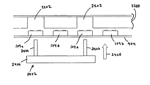
FIG. 24 also shows a punching apparatus 2402 positioned adjacent to
support surface 404, according to an example embodiment of the present
invention. Punching apparatus 2402 includes a body 2404 and a plurality of
punching members 2406. Punching members 2406 are attached to body 2404.
20 In embodiments, punching body 2402 may be any type of applicable punching
device, including a flat surface having punching members 2406 extending
therefrom, or may be a rolling-pin type device with punching members 2406
extending outward radially therefrom. Punching apparatus 2402 may be
configured in additional ways.
In step 2104, all dies of the plurality of dies are simultaneously
transferred into closely adjacent, corresponding empty cells from the support
surface. For example, as shown in FIG. 25, all dies of plurality of dies 104A
are simultaneously being transferred into the corresponding empty cells 2202
of punch tape 2200 by punching apparatus 2402. As shown in FIG. 25,
punching mechanism 2402 has moved upward to push each of the plurality of
dies 104A into their corresponding cells 2202 by pushing through substrate
surface 404. As shown in FIG. 25, substrate surface 404 substantially flexes
to allow punching members 2406 to push plurality of dies 104a upwards
without substantial damage to support surface 404. Although not shown in
FIG. 25, plurality of dies 104a become attached in cells 2202 due to the
adhesiveness of adhesive tape 2304, and remain in cells 2202 after punching
members 2406 are removed or retracted.
In optional step 2106, the punch tape is incremented relative to the
support surface to position each die of another plurality of dies attached to
the
first surface of the support surface closely adjacent to a corresponding empty
cell of another plurality of empty cells in the surface of the punch tape. For
CA 02494487 2005-02-02
WO 2004/012896 PCT/US2003/023792
_ 28 _
example, as shown in FIG.26, punch tape 2200 has been moved and
positioned closely adjacent to plurality of dies 104b such that an empty cell
2202 of punch tape 2200 is closely adjacent to each die of plurality of dies
104b.
Note that the process of incrementing punch tape 2200 relative to
support surface 404 means that any one or more of punch tape 2200, support
surface 404, and/or punching mechanism 2402 may be moved in order to
properly position these elements relative to dies 104 on support surface 404.
In optional step 2108, all dies of the another plurality of dies are
simultaneously transferred from the support surface into closely adjacent
corresponding empty cells. For example, as shown in FIG. 26, punching
mechanism 2402 pushes each die of plurality of dies 104b into the adjacent
cell 2202. Plurality of dies 104b become attached in cells 2202 due to an
adhesiveness of adhesive tape 2304.
In optional step 2110, steps 2106 and 2108 can be repeated until
substantially all dies attached to the support surface have been transferred
from the support surface to the punch tape. Note that optional steps 2106,
2108, and 2110 apply to embodiments where multiple iterations are required
to punch plurality of dies from one surface to another so that all dies
attached
to the first surface are transferred to the second surface. In other words,
for
example, the plurality of dies that are transferred in a single step may be
substantially equal to one out of every N dies of a total number of dies
attached to the support surface. Thus, in such an embodiment, the support
surface may be positioned closely adjacent to the surface of the punch tape,
such that each die of the one out of every N dies attached to the first
surface of
the support surface is closely adjacent to a corresponding empty cell of the
plurality of empty cells in the surface of the punch tape. Hence, the
plurality
of dies are transferred, but not all dies.
In an alternative embodiment, the plurality of dies transferred may be
all of the dies attached to the first surface, so that further iterations are
not
required. For example, FIG. 27 shows a plurality of dies 104 attached to
CA 02494487 2005-02-02
WO 2004/012896 PCT/US2003/023792
-29-
support surface 404, where each die is positioned closely adjacent to
corresponding cell 2202 in punch tape 2200. As shown in FIG. 27, punching
mechanism 2402 has a plurality of punching members 2406 that correspond to
plurality of dies 104. Hence, when punching members 2406 simultaneously
punch upward into support surface 404, all dies of plurality of dies 104 are
moved into corresponding cells 2202 of punch tape 2200, simultaneously.
Note that the punch mechanism die transfer embodiments described
herein are applicable to both pads-up and pads-down die orientations. Hence,
plurality of dies 104 may be transferred into corresponding cells 2202 with
pads facing in or out of the corresponding cells 2202, as desired.
Furthermore,
punching mechanism embodiments may be alternated with adhesive tape
transfer embodiments described above in order to flip the orientation of dies
104. Hence, an adhesive tape may be used to transfer dies one or more times
followed by a final transfer of the plurality of dies 104 by the punching
mechanism. Hence, the adhesive tape embodiments may be used to orient the
dies with either pads up or pads down prior to being punched into cells 2202.
For instance, in an example step 2106, support surface 404 may be
incremented by one column of dies 104 relative to punch tape. Punch tape
2200 may be spooled on a roll. Punch tape 2200 is advanced so that empty die
receptor cells 2202 are aligned over a column of dies 104 on support surface
404. Dies 104 in the column of support surface 404 are punched into the
empty die receptor cells 2202 in step 2108. Support surface 404 may then be
again incremented by one column, and punch tape 2200 is again advanced, so
that the next column of dies 104 of support surface 404 may be punched into
further empty die receptor cells of punch tape 2200. This procedure may be
repeated until support surface 404 is exhausted of dies 104.
Example die transfer embodiments using a punching mechanism are
described in detail in the following subsection.
CA 02494487 2005-02-02
WO 2004/012896 PCT/US2003/023792
-30-
2.1.2.1 Direct transfer from support surface to antenna substrate
According to an embodiment of the present invention, a punching
mechanism may simultaneously transfer each die of a plurality of dies from a
first surface directly onto a corresponding antenna substrate. In embodiments
where the first surface is a support surface that attaches separated dies from
a
wafer, this process allows for extremely rapid fabrication of a large number
of
electronic devices, such as RFID tags 100.
Steps 2102 and 2104 of flowchart 2100 support the transfer for die
from a support surface to a substrate, where instead of using a punch tape as
a
second surface, an substrate is used as the second surface. FIG. 28
illustrates
an example using punching mechanism 2402 to transfer a plurality of dies 104
from a support surface 404 to a substrate structure 2802 that includes a
plurality of tag substrate portions (i.e., tag substrates 116a-d).
As shown in FIG. 28, punclung mechanism 2402 has a plurality of
punching members 2406 that are positioned adjacent to dies 104 on an
opposite surface of support surface 404. In a modified step 2102, support
surface 404 is positioned closely adjacent to a surface of substrate structure
2802, such that each die 104 of the plurality of dies is closely adjacent to a
tag
substrate 116. Each tag substrate 116 has contact areas 210a and 210b for
coupling to contact pads 204a and 204b of each die 104.
Note that an underfill material layer 2804 can be optionally applied to
the surface of substrate structure 2802. This allows for each die 104 to be
underfilled when attached to substrate structure 2802.
Tn a modified step 2104, all dies 104 of the plurality of dies are
simultaneously transferred onto the closely adjacent, corresponding tag
substrate 116 from support surface 404. For example, as shown in FIG. 28,
punching members 2408 may be moved in the direction of arrow 2408 to
transfer dies 104. FIG. 29 shows substrate structure 2802 with each of dies
104 attached to a corresponding one of tag substrates 116a-d. Underfill
material layer 2804 provides for an underfill material to be located between
CA 02494487 2005-02-02
WO 2004/012896 PCT/US2003/023792
-31-
each die 104 and tag substrate 116. Example underfill materials suitable for
underfill material layer 2804 are further described in the following section.
In this manner, a plurality of RFID tags 100 may be rapidly created,
with fewer process steps. Tag substrates 116a-d shown in FIG. 29 may be
subsequently separated to create a plurality of individual RFID tags 100. Note
that while FIGS. 28 and 29 show the transfer of dies 104 directly to tag
substrates 116 in a "pads down" orientation, it will be understood to persons
skilled in the relevant arts) from the teachings herein that this transfer of
dies
104 directly to tag substrates 116 may also be accomplished in a "pads up"
orientation.
2.1.2.2 Underfill Material Embodiments
According to a parallel die punch embodiment of the present invention,
a second surface, such as punch tape 2200, is aligned over separated dies 104
attached to a first surface. Each receptor cell 2202 in punch tape 2202 has a
corresponding die 104 placed therein. Each cell 2202 is then filled with an
underfill material. Punching mechanism 2402 is actuated to move the die 104
from punch tape 2202 onto corresponding tag substrates 116 of substrate
structure 2802. In this manner, any number of dies, including tens and
hundreds of dies, can be transferred simultaneously from punch tape 2200,
instead of merely tx-ansferring one die at a time. Furthermore, by applying
the
underfill material prior to transfernng dies 104 to tag substrates 116, each
die
can be easily underfilled on the respective tag substrate 116 during the
transfer
process, providing numerous advantages.
FIG. 30 shows a flowchart 3000 providing steps for assembling RFID
tags, according to embodiments of the present invention. Note that steps of
flowchart 3000 that are optional are shown enclosed in dotted lines.
Flowchart 3000 will be described in relation to FIGS. 31-47, for illustrative
purposes. Further structural embodiments will be apparent to persons skilled
in the relevant arts) based on the following discussion.
CA 02494487 2005-02-02
WO 2004/012896 PCT/US2003/023792
-32-
Flowchart 3000 begins with step 3002. In step 3002, a plurality of dies
are transferred from a support surface to a chip carrier that has a plurality
of
cells accessible on a first surface of the chip carrier so that each die of
the
plurality of dies resides in a corresponding cell of the plurality of cells
and is
S recessed in the corresponding cell with respect to the first surface. For
example, the chip Garner is a punch tape, such as punch tape 2200 shown in
FIG. 31. As shown in FIG. 31, punch tape 2200 has example empty first and
second cells 2202a and 2202b. FIGS. 32 and 33 show first and second dies
104a and 104b being transferred into first and second cells 2202a and 2202b.
First and second dies 104a and 104b may be transferred into first and second
cells 2202a and 2202b by any process described here or otherwise lmown,
including by a pick and place process. First and second dies 104a and 104b
may be transferred into first and second cells 2202a and 2202b one at a time,
as shown in FIGS. 32 and 33, or simultaneously. Note that two dies are shown
1S in the current example for illustrative purposes, and that the present
invention
is applicable to any number of dies.
In step 3004, an underfill material is applied into each cell of the
plurality of cells. For example, as shown in FIG. 34, an underfill material
3402 is applied into first and second cells 2202a and 2202b to substantially
cover each of dies 104a and 104b, shown as first and second underfill material
portions 3402a and 3402b. Underfill material 3004 is used to underfill dies
104 when attached to a substrate, such as a tag substrate 116, for purposes
such as environmental and hermetic protection, among other reasons.
In embodiments, underfill material 3402 may be any underfill material
2S conventionally known to persons skilled in the relevant art(s). Underfill
material 3402 may be electrically conductive, or electrically non-conductive.
For example, underfill material 3402 may be isotropically conductive, i.e.,
substantially uniformly conductive in all directions. Furthermore, underfill
material 3402 may be anisotropically conductive, i.e., conductive in a desired
direction. For example, underfill material 3402 may be a Z-axis epoxy.
CA 02494487 2005-02-02
WO 2004/012896 PCT/US2003/023792
- 33 -
In an embodiment, the amount of underfill material 3402 applied in
each cell 2202 can be controlled, so that an amount required by the particular
application is present. For example, FIG. 34 shows first and second underfill
material 3402a and 3402b have been applied so that the underfill material
S extends out of first and second cells 2202a and 2202b. In another example,
FIG. 3S shows first and second underfill material 3402a and 3402b have been
applied so that the underfill material is flush or even with the top surface
of
punch tape 2200. For example, in order to cause underfill material 3402 to be
flush or even with the top surface of punch tape 2200, a "squeegee" process
may be used. FIG. 36 shows an example squeegee process being performed.
A squeegee element 3602 is passed along the top surface of punch tape 2200,
smoothing first underfill material 3402a in first cell 2202a, for example. An
excess underfill material 3604 is shown being removed. In the example of
FIG. 36, underfill material 3402 was applied to cells 2202 before squeegee
1S element 3602 was applied. Alternatively, underfill material 3402 may be
applied by squeegee element 3602.
In the example of FIGS. 34-36, a height of each die 104 is
approximately equal to half of a height of the corresponding cell 2202.
Underfill material 3604 fills a remaining half of the height of the cell 2202.
With such an amount of underfill material 3604 in cell 2202 relative to the
size
of die 104, enough underfill material 3604 is present to underfill die 104
when
attached to substrate 116, without having excess underfill material. However,
the present invention is applicable to higher and lower proportions of
underfill
material 3604 in cells 2202.
2S In optional step 3006 of flowchart 3000, the first surface of the chip
carrier is positioned closely adjacent to a surface of a substrate structure
having a plurality of tag substrate portions. For example, FIG. 37 shows an
example substrate structure 2802. Substrate structure 2802 includes a
plurality
of tag substrate portions (i.e., tag substrates 116), also referred to as a
web or
array of tag substrates. Substrate structure 2802 includes any number of tag
substrates I 16, and may be shaped into any size column, row, or array of tag
CA 02494487 2005-02-02
WO 2004/012896 PCT/US2003/023792
-34-
substrates 116. FIG. 38 shows substrate structure 2802 of FIG. 37 after having
been separated into separate strip-shaped tag substrate structures 2802a,
2802b, 2802c, and 2802d. Substrate structure 2802 may be separated into
strips by sawing, cutting, by laser, and by other processes. A strip for
substrate structure 2802 can be conveniently used to transfer dies 104 from
punch tape 2200, wluch typically is also formed in a strip.
FIG. 39 shows a view of a portion of strip-shaped substrate structure
2802a. Substrate structure 2802 includes first and second tag substrates 116a
and 116b. First tag substrate 116a includes an antenna 114a and a guide hole
3902a. Second tag substrate 116b includes an antenna 114b and a guide hole
3902b.
Guide holes 3902 rnay be used to align substrate structure 2802a with
punch tape 2200. For example, guide holes 3902 may be used with guide
holes 2204 shown in FIG. 22 to provide alignment. Guide holes 3902 and
guide holes 2204 may be used to mechanically or optically align substrate
structure 2802a with punch tape 2202. For example, mechanical alignment
can include aligning punch tape 2202 using a first wheel having spaced pegs
that interlock with guide holes 2204, and aligning substrate structure 2802a
using a second wheel having spaced pegs that interlock with guide holes 3902.
The first wheel and second wheel are synchronized.
FIG. 40 shows the top surface of the punch tape 2200 being positioned
closely adjacent to substrate structure 2802a, according to step 3006. Tag
substrate 116a is positioned closely adjacent to cell 2202a.
Tn optional step 3008, a second surface of the chip carrier is punched
proximate to a location opposite of each cell of the plurality of cells to
move
each die out of the corresponding cell such that the underfill material
covering
each die contacts a corresponding tag substrate of the plurality of tag
substrate
portions. For example, as shown in FIG. 41, a punclung member 4102
punches the bottom surface of punch tape 2200 opposite to first cell 2202a.
First die 104 moves out of first cell 2202a towards tag substrate 116a.
Underfill material 3402a contacts tag substrate 116a. As shown in FIG. 42,
CA 02494487 2005-02-02
WO 2004/012896 PCT/US2003/023792
-35-
punching member 4102 moves first die 104 until first die I04 comes into
contact with tag substrate 116a.
In optional step 3010, the first surface of each die is attached to the
corresponding tag substrate so that the at least one contact pad of each die
is
electrically coupled to at least one corresponding contact pad of the
corresponding tag substrate. For example, first die 104 is attached to tag
substrate 116a such that contact pads 204a-d are electrically coupled to
contact
areas 210a-d of tag substrate 116a. First die 104a may be attached to tag
substrate 116a in a variety of ways. Fox example, step 3010 may include the
step where underfill material 3402 is cured to attach each die I04 to the
corresponding tag substrate I16. A curable underfill material 3402 may be
flash curable, thermally curable, acoustically curable, electron beam curable,
ultraviolet (UV) light curable, infrared (llZ) light curable, pressure
curable, and
other type of curable material. Hence, heat, an acoustic source, an electron
beam, UV light, IR light, and/or pressure may be applied as needed to cure
underfill material 3402. A two-party epoxy may be used for a flash curable
underfill material, for example.
In an embodiment, curing of underfill material 3402 causes underfill
material 3402 to contract or shrink. By contracting, underfill material 3402
can cause a decrease in a distance between each die 104 and the corresponding
tag substrate 116, leading to improved mechanical and/or electrical coupling
of contact pads 204a-d of each die 104 to the corresponding contact areas
210a-d of the corresponding tag substrate 116. In such an embodiment,
underfill material 3402 has a thermal coefficient of expansion/contraction
that
2S dictates the amount of contraction when cured. By selecting the material
used
for underfill material 3402, this coefficient can be tuned. Hence, the thermal
coefficient of underfill material 3402 can by tuned to match that of tag
substrate 116, or otherwise. For instance, underfill material 3402 can be
tuned
to contract by a particular amount, such as 2 tunes or 3 times its mass, for
example. Underfill material 3402 caxl be alternatively be tuned to apply a
particular force over an area, such as 50 kg/cm2, for example.
CA 02494487 2005-02-02
WO 2004/012896 PCT/US2003/023792
-36-
For example, the contraction of underfill material 3402 can cause
contact pads 204a-d to come into contact with the corresponding contact areas
210a-d, creating a sufficient electrical connection for operation of the
resulting
device. Contact pads 204a-d and/or contact areas 210a-d may be substantially
uniform in their smoothness or flatness so that a large area may come into
contact between them. In another example, contact pads 204a-d and/or
contact areas 210a-d may be non-uniform in smoothness or flatness to enhance
connectivity. For instance, contact pads 204a-d (and/or contact areas 210a-d)
may have one or more bumps, spikes, peaks, etc. Thus, when contact pads
204a-d come into contact with contact areas 210a-d, the one or more bumps,
spikes, or peaks can partially or completely penetrate or pierce contact areas
210a-d, creating an enhanced electrical and mechanical connection.
In another example, in an embodiment, underfill material 3402
includes electrically conductive microspheres to provide electrical
connectivity. The microspheres may be gold, silver, other metal, or
combination/alloy of metals, for example. Hence, when curing the
contractable underfill material causes the underfill material to contract, a
pressure is created between each die and corresponding tag substrate. The
increased pressure causes the microspheres to form a contact between the die
and substrate, and to defornz, to electrically couple contact pads 204a-d to
contact areas 210a-d.
After die 104a is attached to tag substrate 116a, die 104b can be
similarly attached to tag substrate 116b. Alternatively, dies 104a and 104b
can
be simultaneously attached to their respective tag substrates.
In the example of FIGS. 32-42, dies 104 are oriented to be mounted on
tag substrate 116 in a pads down fashion. FIG. 43-47 shows an example
where dies 104 are oriented to be mounted on tag substrate 116 in a pads up
fashion. For example, as shown in FIG. 43, first and second dies 104a and
104b have been inserted into cell 2202a and 2202b such that contact pads
204a-d face into the cells.
CA 02494487 2005-02-02
WO 2004/012896 PCT/US2003/023792
-37-
As shown in FIG. 44, punch tape 2200 is positioned closely adjacent to
tag substrate 116a of substrate structure 2802a. As shown in FIG. 45, punch
tape 2200 is punched proximate to a location of cell 2202a to move die 104a
out of cell 2202a into a corresponding cell or cavity 4402 in tag substrate
116a
such that underfill material 3402a substantially fills a gap between an outer
edge of die 104a and cavity 4402. As shown in FIG. 45, a surface of die 104a
and a surface of underfill material 3402a is substantially flush or even with
the
surface of tag substrate 116a.
FIG. 46 shows a single die 104 attached in a cavity of tag substrate
116. As shown in FIG. 46, in the current example, contact pads 204a and
204b of die 104 are not electrically coupled to signals of tag substrate 116.
FIG. 47 shows contact pads 204a and 204b of die 104 having been electrically
coupled to contact areas 210a and 210b of tag substrate 116 by first and
second electrical conductors 4702a and 4702b. For example, electrical
conductors 4702 can be printed, applied by a vapor deposition process,
soldered, and otherwise formed between contact pads 204 of each die 104 and
contact areas 210 on the surface of the corresponding tag substrate 116.
2.1.3 Multi-Barrel Die Transfer
According to an embodiment of the present invention, a plurality of
dies 104 may be transferred from a first surface to a second surface using a
multi-barrel die transfer apparatus. FIG. 48A shows an example multi-barrel
die transfer apparatus 4802, according to an embodiment of the present
invention. Multi-barrel die transfer apparatus 4802 includes a body 4804, and
a plurality of barrels 4806. Body 4804 couples barrels 4806 to a gas supply
and vacuum source 4810. For example, a gas such as air, nitrogen, or other
gas may be supplied by vacuum source 4810. In embodiments, any number of
one or more barrels 4806 may be present, but typically multiple barrels 4806
are present to increase the transfer rate of dies 104 by a factor of the
number of
barrels 4806 present. For example, tens or hundreds of barrels may be present.
CA 02494487 2005-02-02
WO 2004/012896 PCT/US2003/023792
-38-
As shown in FIG. 48A, mufti-barrel transfer apparatus 4802 having a
plurality of barrels 4806 is positioned over separated dies 104 attached to a
first surface. The first surface is shown as support surface 404 in the
example
of FIG. 48A. Each barrel 4806 is positioned so that a respective end 4808 of
the barrel 4806 is over a respective die 104 on support surface 404. Multi-
barrel transfer apparatus 4802 receives the dies 104, storing them in stacks
of
dies 104 in the plurality of barrels 4806. As shown in FIG. 48B, mufti-barrel
transfer apparatus 4802 is then positioned over a second surface. The second
surface is shown as transfer surface 1202 in the example of FIG. 48B. Multi-
barrel transfer apparatus 4802 deposits the dies 104 stored in the barrels
4806
on the second surface.
FIG. 49 shows a flowchart 4900 providing example steps for
transferring dies, according to an embodiment of the present invention. For
illustrative purposes, steps of flowchart 4900 may be further described in
regards to mufti-barrel transfer apparatus 4802, as shown in FIGS. 49-52.
However, other structural embodiments will be apparent to persons skilled in
the relevant arts) based on the following discussion. These steps are
described in detail below.
Flowchart 4900 begins with step 4902. In step 4902, each hollow
barrel of a plurality of hollow barrels is applied in parallel to a respective
die
residing on the first surface. For example, FIG. 50 shows a cross-sectional
view of mufti-barrel transfer apparatus 4802 being applied to first surface
802.
The plurality of hollow barrels are barrels 4806. Barrels 4806 are hollow so
that at least a single die 104 may pass into barrel 4806 at a time, and be
stored
therein. As shown in FIG. 48A, each barrel 4806 is applied in parallel with
the other barrels 4806 to a respective die 104 on the first surface.
In step 4904, the respective die is caused to move into each hollow
barrel in parallel. For example, as shown in FIG. 50, each hollow barrel 4806
has a respective die 104 that has moved into the respective hollow barrel
4806.
In step 4906, steps 4902 and 4904 are repeated to create a stack of dies
in each hollow barrel. Hence, for example, mufti-barrel transfer apparatus
CA 02494487 2005-02-02
WO 2004/012896 PCT/US2003/023792
-39-
4802 may be moved as many times as needed to position barrels 4806 over
respective dies so that barrels 4806 may collect the respective dies 104. For
example, as shown in FIG. 50, enough dies 104 have moved into each barrel
4806 to create a stack 5002 of dies 104 in each barrel 4806. Stack 5002 as
shown in FIG. 50 includes two dies 104, but in embodiments may include any
number of dies 104, including tens, hundreds, thousands, and even more dies.
In step 4908, dies from each hollow barrel are deposited in parallel
onto the second surface until the stack of dies in each hollow barrel is
substantially depleted. For example, FIGS. 51 and 52 show cross-sectional
views of mufti-barrel transfer apparatus 4802 being applied to various second
surfaces 804. As shown in FIGS. 51 and 52, barrels 4806 of mufti-barrel
transfer apparatus 4802 are depositing dies 104 in parallel onto second
surface
804. Barrels 4806 deposit dies 104 until they axe substantially depleted of
dies
104. In other words, barrels 4806 can deposit varying amounts of dies 104
onto second surface 804, depending on the number of dies required by second
surface 804, and/or until one or more barrels 4806 are near or completely
depleted of dies 104.
Second surface 804 may have an adhesiveness that allows for dies 104
to stick thereto. For example, second surface 804 may be an adhesive tape, or
may have an adhesive material, such as a wax substance applied thereto to
provide the adhesiveness. As shown in FIG. 51, second surface 804 has cells
5102 formed therein, in which dies 104 are deposited from barrels 4806.
Alternatively, as shown in FIG. 52, second surface 804 may have a
substantially planar surface onto which dies 104 are deposited. Furthermore,
as shown in FIGS. 51 and 52, dies may be deposited in a pads down or pads
up orientation. Barrels 4806 may be reversed end for end after collecting dies
104 in order to change the orientation of dies 104 before being deposited on
second surface 804. For example, ends 4808 and 5004 shown in FIG. 50 may
be reversed after collecting dies 104. Alternatively, barrels 4806 can be left
un-reversed.
CA 02494487 2005-02-02
WO 2004/012896 PCT/US2003/023792
-40-
In an embodiment, a vacuum may be used in steps 4904 and 4908 to
move dies in and out of barrels 4806. For example, a vacuum source 4810 is
shown attached to multi-barrel transfer apparatus 4804 in FIGS. 48A, 48B,
azld 50-51. Vacuum source 4810 may be applied to multi-barrel transfer
apparatus 4804 to cause a vacuum or suction in one or more barrels 4806 to
move respective dies 104 into the barrels) 4806. The vacuum or suction may
be continuous or applied in controlled bursts. Vacuum source 4810 may also
be applied or varied to move dies 104 out of barrels 4806 onto second surface
804. For example, vacuum source 4810 may apply bursts of positive pressure
to move individual dies 104 out of barrels 4806.
Barrels 4806 may be configured to allow for proper application of
vacuum source 4810. FIG. 53 shows a cross-sectional top view of an example
barrel 4806 with die 104 inside, according to an embodiment of the present
invention. Barrel 4806 may be rectangular as shown in FIG. 53, or may be
round, or other shapes. Barrel 4806 may have a smooth interior surface 5302
in an embodiment of the present invention. Alternatively, as shown in FIG.
53, interior surface 5302 may have a channel 5304 formed in one or more
corners to allow gas to pass around dies 104. Channels 5304 may be used to
control the vacuum or pressure in barrels 4806.
Barrels 4806 may be made from a metal, plastic, or other applicable
material. For example, barrels 4806 may be barrels, tubes, or needles similar
to hypodermic needles. Barrels 4806 are configured to collectively hold any
number of dies 104. In an embodiment, the number and length of each barrel
4806 will be configured to have a cumulative die 104 holding capacity of at
least one wafer worth of dies 104. For example, the cumulative holding
capacity may be on the order of 50,000 to 100,000 of dies 104.
The filled multi-barrel die collet can be moved, robotically or
otherwise, to a die dispensing station for tag assembly. An empty mufti-barrel
die collet can then be positioned adjacent to a new wafer of separated die on
a
support surface to repeat the process.
CA 02494487 2005-02-02
WO 2004/012896 PCT/US2003/023792
-41 -
Note that other mechanisms and/or processes may alternatively be used
in step 4904 to cause dies to move into each hollow barrel, and in step 4908
to
deposit dies from each hollow barrel. For example, mechanical structures and
forces, chemical processes and forces, electrostatic forces, adhesive
materials,
a gas pressure system, and further mechaiusms and processes may be used, as
would be understood by persons skilled in the relevant arts) from the
teachings herein.
2.1.4 Die Transfer Using a Die Frame
According to an embodiment of the present invention, a plurality of
dies 104 may be transferred to a target surface using a "die frame" or "wafer
tape." The die frame or wafer tape is formed directly from a wafer to hold the
dies of the wafer such that they may be easily transferred to the target
surface.
Dies may be transferred from the die frasne/wafer tape to an intermediate
surface, or directly to a final surface, such as a substrate. Thus, the die
frame
or wafer tape of the present invention allows for fewer required manufacturing
steps when transferring dies to a substrate compared to conventional transfer
processes. For example, in a typical conventional process, dies are
individually transferred from the wafer to an intermediate transfer surface by
a
pick-and-place machine. The dies are then transferred from the intermediate
surface to the final destination surface. This two step process allows for the
dies to be flipped. According to the present invention, dies can be directly
transferred from the die frame/wafer tape to a substrate, without transfer to
an
intermediate surface. Furthermore, the dies can be flipped or not flipped by
the transfer, as needed.
Note that the die frame/wafer tape of the present invention is referred
to below as a die frame, for ease of description. The die frame may be formed
according to processes of the present invention, some examples of which are
described below for purposes of illustration, and not limitation. FIGS. 57A
and 57B show flowcharts for making a die frame, according to example
embodiments of the present invention. Further embodiments for the die frame
CA 02494487 2005-02-02
WO 2004/012896 PCT/US2003/023792
-42-
of the present invention, and for making the die frame of the present
invention,
will be apparent to persons skilled in the relevant arts based on the
following
discussion. Furthermore, FIGS. 66 and 68A-B show example flowcharts for
transferring dies using a die frame, according to example embodiments of the
present invention. Further embodiments for transferring dies using the die
frame of the present invention will be apparent to persons skilled in the
relevant arts based on the discussion herein.
FIG. 57A shows a flowchart 5700 providing example steps for making
a die frame, according to an embodiment of the present invention. Flowchart
5700 will be described below in relation to FIGS. 58-63, for illustrative
purposes. Flowchart 5700 begins with step 5702. In step 5702, a ring shaped
groove is formed in a first surface of a wafer around a plurality of dies
formed
in the first surface of the wafer. For example, FIG. 58 shows an example
wafer 5800. As shown in FIG. 58, a ring shaped groove 5802 has been formed
in a surface of wafer 5800 closely adjacent to an outer edge of wafer 5800.
For example, the depth of ring shaped groove 5802 may be approximately
equal to the thickness of an integrated circuit die, such as die 104, that is
formed in the surface of wafer 5800 (not shown in FIG. 58). In the example of
FIG. 58, ring shaped groove 5802 is substantially round or elliptical, and is
continuous. In alternative embodiments, ring shaped groove 5802 may be
formed in other shapes, including square or other polygon. Furthermore, ring
shaped groove 5802 does not necessarily have to be continuous, as shown in
the example of FIG. 58, but may be instead be non-continuous, and for
example, may include two or more separate portions formed in the surface of
wafer 5800.
In step 5704, the first surface of the wafer is scribed to form a grid of
grooves in the first surface of the wafer that separates the plurality of
dies. For
example, FIG. 59 shows wafer 5800 after having been scribed. The scribing
of wafer 5800 has created a grid 5902 in the surface of wafer 5800. Grid 5902
is formed from a plurality of horizontal and vertical grooves 5904 formed in
the surface of wafer 5800. Fox example, a first groove 5904A, a second
CA 02494487 2005-02-02
WO 2004/012896 PCT/US2003/023792
-43-
groove 5904B, a third groove 5904C, and a fourth groove 5904D of grid 5902
are indicated in FIG. 59. Within grid 5902 resides a plurality of areas of the
surface of wafer 5800 in which dies 104 may reside. For example, FIG. 59
shows an area for a first die 104a and an area for a second die 104b that
reside
within grid 5902. Note that features of dies 104 are not shown in FIG. S8 and
FIG. 59.
FIG. 60 shows a cross sectional view of a portion of wafer 5800. As
shown in FIG. 60, ring shaped groove 5802 and grooves 5904a and 5904b
have a thickness or depth of depth 6002. For example, depth 6002 may be 100
micrometers, or other thickness. Depth 6002 is typically equal to or greater
than a thickness of a die of wafer 5800. As shown in FIG. 60, wafer 6004 has
a thickness 6004. Thickness 6004 can be any thickness of a conventional or
special purpose wafer, which may be 600 to 700 micrometers or other
thickness, for example.
1S In step 5706, a solidifiable material is applied to the first surface of
the
wafer to substantially fill the ring shaped groove and the grooves of the
grid.
FIG. 61 shows, for example, a solidifiable material 6102 that has been applied
to the surface of wafer 5800 to substantially fill ring shaped groove 5802 and
grooves 5904 of grid 5902. Solidifiable material 6102 substantially fills ring
shaped groove 6102 and grooves 5904. For example, solidifiable material
6102 may fill the grooves to a level below the surface of wafer 5800, to the
same level as the surface of wafer 5800 (as shown in FIG. 62), or even to
slightly protrude above the surface of wafer 5800. Solidifiable material 6102
may be a polymer, epoxy, resin, urethane, glass, or other material, for
example.
A variety of processes may be used to cause solidifiable material 6102
to fill grooves 5802 and 5904 when applied to wafer 5800, without leaving a
substantial excess amount of solidifiable material 6102 otherwise on the
surface of wafer 5800. For example, a vacuum source may be applied to the
opposite surface of wafer 5800, or to a tape, such as a blue or green tape, to
which wafer 5800 is attached, to cause solidifiable material 6102 to be pulled
CA 02494487 2005-02-02
WO 2004/012896 PCT/US2003/023792
-44-
into grooves 5802 and 5904. In another embodiment, a gas source may direct
a gas towards the surface of wafer 5800 to which solidifiable material 6102 is
being applied, to blow, force, or push solidifiable material 6102 into grooves
5802 and 5904. In another embodiment, solidifiable material 6102 is applied
to the surface of wafer 5800 in a spin-coating fashion, such that a spinning
motion of wafer 5800 causes solidifiable material 6102 to move or "wick" into
grooves 5802 and 5904. Solidifiable material 6102 may be applied in
additional ways to fill grooves 5802 and 5904, including by "squeegee"
application, spraying, vapor deposition, physical deposition, or chemical
deposition.
In step 5708, the solidifiable material is caused to harden into a ring
shaped hardened material in the ring shaped groove, and into a grid shaped
hardened material in the grooves of the grid to form the die frame. For
instance, in the example of FIGS. 61 and 62, solidifiable material 6102 is
1S caused to hardened in ring shaped groove 5802, and in grooves 5904 of grid
5902. In an embodiment, the hardened material is formed by causing
solidifiable material 6102 to hardened by a curing process. Hence,
solidifiable
material 6102 may be any curable material, such as a curable polymer, epoxy,
resin, urethane, glass, or other material, for example. Solidifable material
6102 may be a material that is caused to harden in a variety of ways,
including
by heat, by allowing a sufficient amount of time for solidifiable material
6102
to hardened on its own, by applying light, or by other ways described
elsewhere herein or otherwise known.
In step 5710, the wafer is thinned such that the grid shaped hardened
2S material removably holds the plurality of dies. For example, FIG. 63 shows
a
die frame 6300 formed according to the present invention. Die frame 6300
includes a hardened material 6304 resulting from the hardening of solidifiable
material 6102 in ring shaped groove 5802 and grooves 5904 of grid 5902, as
described above. Die frame 6300 further results from the thinning of wafer
5800. As shown in FIG. 63, wafer 5800 has been thinned to form die frame
6300 of a thickness of approximately depth 6002. In embodiments, die frame
CA 02494487 2005-02-02
WO 2004/012896 PCT/US2003/023792
-45-
6300 can be formed or thinned to have a thickness of approximately equal to
depth 6002, or a lesser thickness. Thus, because die frame 6300 has a
thickness approximately equal to or less than depth 6002, die frame 6300
removably holds dies 104 in corresponding openings 6302. In other words,
dies 104 can be easily removed from openings 6302. For example, as shown
in FIG. 63, die frame 6300 removably holds die 104A in opening 6302A, and
removably holds die 104B in an opening 6302B. Die frame 6300 provides a
support structure in the shape of ring shaped groove 5802 and grid 5904 that
is
capable of removably holding dies 104 in openings 6302. Dies 104 may be
removed from die frame 6300 by pushing, poking, or otherwise forcing them
out of openings 6302 from either surface of die frame 6300 onto another
surface. Depending on which surface of die frame 6300 that dies 104 are
forced from will determine Whether dies 104 are transferred to a surface in
either a pads up or a pads down orientation.
Note that wafer 5800 may be thinned in step 5710 according to any
conventional or otherwise known means. Furthermore, note that solidifiable
material 6102 is selected so that it does not substantially adhere to die 104,
so
that dies 104 may be easily removed from die frame 6300 and are thus
removably held therein.
FIG. 57B shows a flowchart 5720 providing example steps for making
a die frame, according to another embodiment of the present invention.
Flowchart 5720 will be described below in relation to FIGS. 64A-64C, 65A,
and 65B, for illustrative purposes. Flowchart 5720 begins with step 5722. In
step 5722, a wafer attached to an adhesive surface is scribed such that a
resulting plurality of dies are separated by a grid of grooves that extend
through the wafer to the adhesive surface. For example, FIG. 64A shows a
scribed wafer 6402 attached to an adhesive surface 6404. Adhesive surface
6404 is held in a wafer frame 6406. Wafer frame 6406 may also be referred to
as a wafer carrier or tape ring. For example, adhesive surface 6404 may be a
green tape, blue tape, or other adhesive surface type. Wafer frame 6406 holds
and supports adhesive surface 6404 in a taut fashion so that scribed wafer
CA 02494487 2005-02-02
WO 2004/012896 PCT/US2003/023792
-46-
6402 may be accessed. Because wafer 6402 has been scribed, wafer 6402 has
a grid 5902 of grooves 5904 (not shown in FIG. 64A) that separates the dies
104 of wafer 6402. Wafer 6402 is scribed so that grooves 5904 extend
through wafer 6402 to adhesive surface 6404. Hence, dies 104 of wafer 6402
are individually attached to adhesive surface 6404. FIG. 64B shows a cross-
sectional view of an example scribed wafer 6402 having three dies 104
separated by grooves 5904. Note that wafer 6402 is shown with three dies 104
for purposes of illustration, and not of limitation. FIG. 64C shows a
perspective view of a portion of an example scribed wafer 6402 attached to
adhesive surface 6404, having a plurality of dies 104 separated by grooves
5904 of grid 5902.
In step 5724, a solidifiable material is applied to the scribed wafer to
substantially fill the grooves of the grid. For example, as shown in FIG. 65A,
solidifiable material 6102 is applied to scribed wafer 6402 to partially or
completely fill grooves 5904 between dies 104. As shown in FIG. 65A,
solidifiable material 6102a fills grooves 5904 between dies 104. In an
embodiment, solidifiable material 6102 may be applied such that solidifiable
material 6102b is present to fill a space 6500 on adhesive surface 6404
between an outer edge 6502 of wafer 6402 and an inner edge 6504 of wafer
frame 6406. Note that in an embodiment, solidifiable material 6102 may even
extend partially within wafer frame 6406, as shown in FIG. 65A, although this
is not required. Solidifiable material 6102 may be applied in any manner
described elsewhere herein, such as is described above in relation to FIGS. 61
and 62, or otherwise known.
In step 5726, the solidifiable material is caused to harden into a grid
shaped hardened material in the grooves of the grid. For example, solidifiable
material 6102a and 6102b shown in FIG. 65A is caused to harden into a grid
shaped hardened material, such as is described above for hardened material
6304 in relation to FIG. 63.
In step 5728, the adhesive surface is removed so that the grid shaped
hardened material removably holds the plurality of dies. For example, FIG.
CA 02494487 2005-02-02
WO 2004/012896 PCT/US2003/023792
-47-
65B shows a die frame 6300 that results from the removal of adhesive surface
6404. Hardened material 6304a is present between dies 104, and hardened
material 6304b is present outside of dies 104. Hardened material 6304
removably holds dies 104 in the shape of a grid in die frame 6300, as
described above. Note that adhesive surface 6404 may be removed or
detached by peeling, chemically dissolving, or otherwise removing it from die
frame 6300.
Note that die frame 6300 may be formed in a pads up or pads down
fashion. For example, flowchart 5720 may include steps similar to steps 702,
20 704, and 706 shown in flowchart 700 of FIG. 7, for flipping the orientation
of
dies 104 prior to performance of step 5722. Thus, the pads of dies 104 may be
facing toward or away from adhesive surface 6404, depending on which
orientation is selected.
The structure of die frame 6300 has numerous advantages. For
example, the portion of die frame 6300 formed in a ring shape in ring shaped
groove 5802 allows for a holding mechanism, such as a clamp or jig, to
reliably hold die frame 6300 when being used for transferring dies, for
example. The portion of die frame 6300 formed in a grid shape in grid 5904
allows for the holding of dies 104, with relative ease in removal of dies 104,
as
described below. The structure of die frame 6300 has further benefits. Note
that in some embodiments, the ring shaped portion of die frame 6300 may not
be necessary, and is not present.
Preferably, excess solidifiable material 6102 is not left on the surface
of wafer 5800. In embodiments, flowchart 5700 may include an additional
step that is performed prior to step 5704, where a layer of protective
material
is applied onto the surface of the wafer. The protective material, for
example,
may be a photo-resist material, or other protective material, which may be
spin
coated or otherwise applied to the surface of the wafer. Thus, in an
embodiment, flowchart 5700 may also include the step where the protective
material is removed from the surface of the wafer. For example, removing the
protective material from the wafer can cause the removal of excess
solidifiable
CA 02494487 2005-02-02
WO 2004/012896 PCT/US2003/023792
-48-
material 6102 in its hardened state or in its unhardened state (i.e., prior to
or
after step 5708). For example, wafer 5800 may be immersed in a solvent, or
may have a solvent applied thereto to dissolve the protective material from
the
surface of wafer 5800. The protective material may be removed from 5800 by
S other ways that are known to persons skilled in the relevant arts.
Die frame 6300 may be used to transfer dies 104 to a subsequent
destination or transfer surface. The subsequent surface can be an intermediate
surface, such as a blue or green tape, or intermediate surfaces otherwise
known or described elsewhere herein, or may be used to transfer dies 104 to a
final destination surface, such as a substrate. Furthermore, die frame 6300
allows for precise transfer of dies. For example, because the location of dies
removably held in die frame 6300 is accurately known, precise registration of
dies is present. Thus, expensive optical and/or other type registration
systems
may not be required to locate and accurately place dies.
1S FIG. 66 shows a flowchart 6600 providing steps for transferring a
plurality of dies to a surface using a die frame, according to embodiments of
the present invention. Note that steps of flowchart 6600 that are optional are
shown enclosed in dotted lines. Flowchart 6600 will be described in relation
to FIG. 67, for illustrative purposes. Further structural embodiments will be
apparent to persons skilled in the relevant arts based on the following
discussion.
Flowchart 6600 begins with step 6602. In step 6602, a die frame is
positioned closely to a surface of a substrate tape that includes a plurality
of
substrates such that a die of a plurality of dies removably held in the die
frame
2S is closely adjacent to a corresponding substrate of the plurality of
substrates of
the substrate tape. For example, FIG. 67 shows a system 6700 for transferring
dies to a surface using die frame 6300. System 6700 includes die frame 6300,
punching member 2406, a die frame jig 6702, a first reel 6706, a second reel
6708, and a substrate tape 6710. As shown in FIG. 67, substrate tape 6710
includes a plurality of substrates 6712a-c. Substrate tape 6710 may include
any number of substrates 6712. As shown in FIG. 67, die frame 6300 is
CA 02494487 2005-02-02
WO 2004/012896 PCT/US2003/023792
-49-
positioned closely adjacent to a surface of substrate tape 6710. Die frame
6300 is positioned closely adjacent to substrate tape 6710 such that a die 104
may be punched from die frame 6300 to a substrate 6712 of substrate tape
6710, as is described below.
In step 6604, the die is transferred onto the closely adjacent
corresponding substrate from the die frame. As shown in FIG. 67, die 104 has
been transferred from die frame 6300 to a surface of substrate 6712b of
substrate tape 6710. For example, as shown in FIG. 67, die 104 may be
punched from die frame 6300, which removably holds die 104, onto substrate
6712a. For example, a punching mechanism 2406 may be used to punch die
104 from die frame 6300 onto substrate 6712a. In further embodiments, other
mechanisms may be used to transfer die 104 from die frame 6300 to a
substrate 6712.
Multiple dies may be transferred from die frame 6300 to substrate tape
1 S 6710 in this manner. In step 6606, the substrate tape is incremented. For
instance, as shown in the example of FIG. 67, substrate tape 6710 may include
a plurality of substrates 6712 that are serially arranged. Substrate tape 6710
may be incremented according to a reel-to-reel system, such as shown in FIG.
67. In FIG. 67, a first reel 6706 may supply substrate tape 6710 to a second
reel 6708, which receives substrate tape 6710. By turning frst and second
reels 6706 and 6708, substrate tape 6710 may be incremented to move a next
substrate 6712 into position to receive a die 104 from die frame 6300. Other
mechanisms may be used to increment substrate tape 6710. Furthermore, in
alternative embodiments, substrate tape may include an N x M array of
substrates 6712, where N > 1 and M > l, instead of having substrates 6712
serially aligned.
In step 6608, the die frame is positioned closely adjacent to the surface
of the substrate tape such that another die of a plurality of dies removably
held
in the die frame is closely adjacent to a next corresponding substrate of the
plurality of substrates of the substrate tape. For example, shown in FIG. 67,
die frame 6300 is held in a die frame jig 6702. Die frame jig 6702 may be
CA 02494487 2005-02-02
WO 2004/012896 PCT/US2003/023792
-50-
moved laterally relative to substrate tape 6710 to position the next die 104
over the next substrate 6712, such as substrate 6712a or 6712b. Because the
size of a die 104 is well known, the die frame jig 6702 may be repositioned by
the width or length of a die 104, instead being repositioned by an optical
and/or other registration system type which has to determine the location of a
die. Fox example, in an embodiment, for a 500 x 500 micron sized die, die
frame jig 6702 may be moved by 500 microns (possibly plus the width of a
groove 5904) to place the next die 104 into position for transfer. Note that
the
present invention is applicable to any size die.
In step 6610, another die is transferred onto the closely adjacent next
corresponding substrate from the die frame. Thus, in this manner a plurality
of dies 104 may be transferred from die frame 6300 on to corresponding
substrates 6712 of substrate tape 6710. In this manner, for example, a large
number of tag substrate/die combinations may be created in a relatively rapid
fashion, in fewer steps than with conventional processes.
Note that multiple die frames 6300 may be placed in a stack, from
which dies 104 may be transferred to a destination surface. The dies 104 may
be transferred from the stack of die frames 6300 to the destination surface
using a punching mechanism, a vacuum/gas source, and any other mechanism
described elsewhere herein or otherwise known. For example, FIG. 68A
shows a flowchart 6800 providing steps for transferring a plurality of dies to
a
surface using a stack of die frames, according to another embodiment of the
present invention. ~ Note that steps of flowchart 6800 that are optional are
shown enclosed in dotted lines. Further structural embodiments will be
apparent to persons skilled in the relevant arts based on the following
discussion.
Flowchart 6800 will be described in relation to FIG. 69, for illustrative
purposes. Flowchart 6800 begins with step 6802. In step 6802, a stack of die
frames is formed, each die frame including a grid having a plurality of
rectangular openings, wherein each opening of the plurality of rectangular
openngs removably holds a die, wherein corresponding rectangular openings
CA 02494487 2005-02-02
WO 2004/012896 PCT/US2003/023792
-51 -
of the die frames in the stack are aligned in a column to form a plurality of
columns of openings. For example, FIG. 69 shows a stack of die frames 6902.
Stack 6902 includes a plurality of die frames 6300. For illustrative purposes,
stack 6902 is shown including six die frames 6300a-f, but may include any
number of two or more die frames 6300. As described above, each die frame
6300 includes hardened material 6304 shaped in the form of grid 5902. A
plurality of openings 6302 are present in each die frame 6300, each removably
holding a die 104. Die frames 6300 are aligned so that corresponding
openings 6302 form columns in the stack 6902 (not shown in FIG. 69).
In step 6804, a die removably held in an opening is transferred from at
Ieast one column of the plurality of columns to the destination surface. In
other words, one or more dies 104 are transferred from stack 6902 from one or
more columns to the destination surface. Dies 104 may be transferred in
numerous ways from stack 6902. For example, as shown in FIG. 69, one or
more punching members 2406 may be applied to corresponding columns of
openings 6302 in stack 6902. A punching member 2406 pushes through stack
6902 to move dies 104 from the respective column of openings 6302 in stack
6902 to the destination surface. A punching member 2406 may be stepped to
push out a single die 104 at a time. Any number of punching members 2406
may operate in parallel, such as punching members 2406a-c as shown in the
example of FIG. 69, to increase the rate of die transfer.
Other processes for transferring dies 104 from stack 6902 may be used,
including the use of a gas or vacuum source to apply gas pressure,
electrostatic
force, pick and place devices, and processes described elsewhere herein, or
otherwise known. Another example such process is described in detail below
with respect to FIG. 68B.
Note that the destination surface may be a substrate tape or structure,
as shown in FIG. 69. Alternatively, the destination surface may be a punch
tape or chip carrier, such as shown in FTG. 22, any intermediate surface, such
as a green tape or blue tape, or any other surface. Furthermore, dies 104 may
be transferred to the destination surface in a pads up or down configuration,
CA 02494487 2005-02-02
WO 2004/012896 PCT/US2003/023792
-52-
depending on the orientation of staclc 6902. Stack 6902 may be inserted into a
die deposition apparatus that holds and aligns the respective die frames 6300
in a stack, and allows dies to be transferred therefrom.
Further detail for an example embodiment of flowchart 6800 is shown
in FTG. 68B. FIG. 68B will be described in relation to FIG. 70, for
illustrative
purposes. FIG. 70 shows a system 7000 for transfernng dies from a die frame
6300 using a multi-barrel die transfer apparatus 4802, according to an
embodiment of the present invention. As shown in FIG. 70, multi-barrel die
transfer apparatus 4802 .includes a plurality of barrels 4806a-c. Furthermore,
system 7000 includes a stack 6902 of die frames 6300 which includes first,
second, third, and fourth die frames 6300a-d. Stack 6902 may include any
number of die frames 6300.
In step 6802, a stack of die frames is formed, each die frame including
a grid having a plurality of rectangular openings, wherein each opening of the
plurality of rectangular openings removably holds a die, wherein
corresponding openings of the die frames in the stack are aligned in a column.
As shown in FTG. 70, for example, the die frames 6300a-d of die frame stack
6902 are aligned such that a plurality of columns 7002 are formed. Each
column 7002 includes a die removably held in an opening in each of die
frames 6300a-d.
In step 6812, each hollow baxrel of a plurality of hollow barrels is
applied to a respective column of openings of the stack of die frames. For
example, as shown in FIG. 70, a first column 7002a has first barrel 4806a
applied thereto, a second column 7002b has second barrel 4806b applied
thereto, and a third column 7002c has a third barrel 4806c applied thereto.
In step 6814, dies removably held in the openings of the respective
column of openings are caused to move into each hollow barrel in paxallel. As
shown in FIG. 70, dies 104 that were removably held in die frames 6300a-
6300d are caused to move into barrels 4806. Dies 104 may be caused to move
into the hollow barrels 4806 by vacuum, by gas pressure, by mechanical
means, or other means described elsewhere herein or otherwise known.
CA 02494487 2005-02-02
WO 2004/012896 PCT/US2003/023792
-53-
In step 6816, steps 6812 and 6814 are repeated until each hollow barrel
contains a stack of dies of a predetermined number. For example, steps 6812
and 6814 may be repeated until one or more of barrels 4806a-c become full,
until stack 6902 is depleted of dies, or when an arbitrary number of dies 104
have been moved from stack 6902.
In step 6818, a die from each hollow barrel is deposited onto the
surface until the stack of dies contained by each hollow barrel is
substantially
depleted. Thus, dies 104 from hollow barrels 4806 may be deposited onto the
destination or target surface, until the dies 104 in hollow barrels 4806 are
depleted, or until the surface is full of dies 104, or until an arbitrary
number of
dies 104 have been transferred. As described above, dies 104 may be
deposited from hollow barrels 4806 by mechanical means, by vacuum, by gas
pressure or by other means described elsewhere herein or otherwise known.
Hence, die frame 6300 may be used in a variety of ways to transfer
dies to a target surface. Furthermore, die frame 6300 may be combined with
any of the other die transfer mechanisms and processes described elsewhere
herein to provide for enhanced die transfer mechanisms and processes.
Further example die frame embodiments are described in the following
subsections, for illustrative purposes.
2.1.4.1 Die Frame Formed in a Tape Structure
In an embodiment, a die frame may be formed in a flexible, planar tape
structure, similar to a "blue tape" or "green tape" used to attach
wafers/dies.
The tape structure is fabricated to include a hardenable material or
substance.
A wafer is attached to the tape structure, and is separated into a plurality
of
dies. The tape structure is processed to cause a hardened grid structure to
form in the tape structure, which removably holds the plurality of dies. FIG.
71 shows a flowchart 7100 providing steps for making such a die frame or die
support frame, according to an example embodiment of the present invention.
Flowchart 7100 is described below in relation to FIGS. 72, 73A, 73B, and 74
for illustrative purposes.
CA 02494487 2005-02-02
WO 2004/012896 PCT/US2003/023792
-54-
Flowchart 7100 begins with step 7102. In step 7102, a wafer that
comprises a plurality of dies is attached to a surface of a tape structure.
For
example, as described above, FIG. 4B shows a wafer 400 attached to an
example support surface 404. As shown in FIG. 4A, wafer 400 includes a
plurality of dies 104. In the present embodiment, wafer 400 is attached in a
similar fashion to a tape structure. The surface of the tape structure and/or
wafer 400 may have an adhesive material applied thereon to adhere wafer 400
to the tape structure. The tape structure is described in further detail
below.
In step 7104, a grid of grooves is formed in the wafer to separate the
plurality of dies on the surface of the tape structure. For example, FIG. 72
shows wafer 400 attached to a surface 7202 of a tape structure 7200, according
to an example embodiment of the present invention. Wafer 400 is separated
into a plurality of dies 104 on surface 7202. Wafer 400 may be separated into
a plurality of dies 104 on tape structure 7200 according to any conventional
wafer separation technique, including scribing or separating wafer 400 by
sawing, laser, mechanical or chemical etching, and other techniques. The
separation of wafer 400 creates grid 5902 of grooves 5904 in wafer 400.
Tape structure 7200 is a flexible structure that comprises a hardening
or solidifiable material that can be caused to harden by various techniques.
For example, tape structure 7200 may include a material that can be caused to
harden by the application of light, including by application of ultraviolet
(TJV)
or other frequency bands of light. Alternatively, tape structure 7200 may
include a material that may be caused to harden by the application of a solid,
liquid, or gas, that reacts with the material of tape structure 7200 to cause
25. portions of tape structure 7200 to harden or solidify.
All or a portion of tape structure 7200 may comprise the material that
can be caused to harden. For example, FIG. 73A shows a cross-sectional view
of tape structure 7200 as a single layer structure having the solidifiable or
hardenable material throughout. Alternatively, FIG. 73B shows tape structure
7200 as a mufti-layer structure that includes a solidifiable or hardenable
material Iayer 7302. Layer 7302 can be fabricated into tape structure 7200, or
CA 02494487 2005-02-02
WO 2004/012896 PCT/US2003/023792
-55-
can be spread, applied, or sprayed onto tape structure 7200. For example, the
solidifiable or hardenable material may be a photoresist material or an epoxy
applied to tape structure 7200. Tape structure 7200 may further include a
paper, tape, polymer, or other material layer to provide structural support.
Note that steps 7102 and 7104 may be performed by structures)
described herein or otherwise known, and may be performed by the same
structure, or different structures. For example, a wafer preparation module
may perform steps 7102 and 7104. An example such wafer preparation
module is further described in sections 3.0-3.2 below. The wafer preparation
module may include a wafer application apparatus, for applying a wafer to
tape structure 7200, andlor may include a wafer singulation apparatus for
separating/singulating the wafer on surface 7202.
In step 7106, a portion of the tape structure that is accessible through
the grooves of the grid is caused to harden into a grid shaped structure. For
example, FIG. 74 shows an example system 7400 for causing the portion of
tape structure 7200 that is accessible through grooves 5904 of grid 5902 to
harden into a grid shaped structure. As shown in FIG. 74, a hardening agent
source 7402 transmits a hardening agent 7404 towards separated wafer 400
and tape structure 7200. Due to the location of dies 104, hardening agent 7404
reaches tape structure 7200 through grooves 5904 and at peripheral areas.
Thus, portions of tape structure 7200 that are accessible through grooves 5904
and in peripheral areas are caused to harden, shown as hardened groove
portions 7410 and hardened peripheral areas 7420, respectively. Portions of
tape structure 7200 that are not accessible to hardening agent 7404 (due to
the
2S application of hardening agent 7404 being blocked by dies 104) do not
harden.
For example, FIG. 74 shows an example portion 7430 of tape structure 7200
that is not hardened.
Hardening agent source 7402 can include various sources for
hardening agents, depending on the type of hardening or solidifiable material
in tape structure 7200. For example, hardening agent source 7402 can include
a light source and respective optics, including a W light source or infrared
CA 02494487 2005-02-02
WO 2004/012896 PCT/US2003/023792
-56-
(IR) light source, for a material that hardens with exposure to light. For
example, the hardening material may be a photoresist material. In such an
embodiment, hardening agent 7404 may be light, such as UV, IR, or other
frequency band of light.
Alternatively, hardening agent source 7402 can include a gas or liquid
supply for applying or spraying a gas or liquid towards separated wafer 400
and tape structure 7200. For example, hardening agent 7404 may be an epoxy
of a two-party epoxy, to react with a corresponding epoxy incorporated in tape
structure 7200. Other hardening agent sources and hardening agents are
applicable to the present invention, including a heat source.
A die frame 7460 is thereby formed. The die frame 7460 formed
according to flowchart 7100 removably holds the plurality of dies 104. Thus,
one or more dies 104 of the plurality of dies 104 can be moved from the grid
shaped structure of die frame 7460 onto a target surface. FIG. 75 shows a die
frame 7460 that includes an example grid shaped stt-~xcture 7500. Die frame
7460 is held by a die frame jig 6702. As shown in FIG. 75, a die 104 is being
moved from die frame 7460 to a substrate 6712. In the example of FIG. 75,
die 104 is being moved by a punching member 2406. Die 104 may be moved
from die frame 7460 in a variety of ways, including by punching, by action of
a gas, and by other ways otherwise knouni or described elsewhere herein.
Note that each non-hardened area 7430 may or may not tear from die
frame 7460 when the respective die 104 is moved from die frame 7460.
Die frame 7460 may be used in a variety of ways to transfer dies 104
to a target surface, including any of the ways for transferring dies described
elsewhere herein. Furthermore, die frame 7460 may be combined with any of
the other die transfer mechanisms and processes described elsewhere herein to
provide for enhanced die transfer mechanisms and processes.
CA 02494487 2005-02-02
WO 2004/012896 PCT/US2003/023792
-57-
2.1.4.2 Die Frame Formed by Releasing Encapsulated
Hardenable Material
Tn an embodiment, a die frame may be formed on a planar tape
structure, similar to a "blue tape" or "green tape" used to attach
wafers/dies.
The tape structure is fabricated to include an encapsulated, releasable
material
or substance that hardens. A wafer is attached to the tape structure, and is
separated into a plurality of dies. The process of separating the wafer into
dies
breaches the tape structure, which releases the encapsulated material. The
released material hardens to create a hardened grid structure on the tape
structure, which removably holds the plurality of dies. The remainder of the
tape structure may then be optionally removed. FIG. 76 shows a flowchart
7600 providing steps for making such a die frame or die support frame,
according to an another example embodiment of the present invention.
Flowchart 7600 will be described below in relation to FIGS. 77-82, for
illustrative purposes.
Flowchart 7600 begins with step 7602. In step 7602, a wafer that
comprises a plurality of dies is attached to a surface of a tape structure,
wherein the tape structure comprises an encapsulated releasable hardening or
hardenable material. For example, as described above, FIG. 4B shows wafer
400 attached to an example support surface 404. As shown in FIG. 4A, wafer
400 includes a plurality of dies 104. In the present embodiment, wafer 400 is
similarly attached to a tape structure. However, in the current embodiment,
the tape structure comprises an encapsulated hardening or solidifable material
that can be released and hardened.
For example, FIG. 77 shows wafer 400 attached to a surface 7706 of a
tape structure 7702. Surface 7706 and/or wafer 400 may have an adhesive
material applied thereto to adhere wafer 400 to surface 7706.
Tape structure 7702 may be a single or multi-layer structure. An
example multi-layer structure for tape structure 7702 is shown in FIG. 77. As
shown in FIG. 77, tape structure 7702 includes a layer 7704. Layer 7704
comprises an encapsulated hardening material that can be released and
CA 02494487 2005-02-02
WO 2004/012896 PCT/US2003/023792
-58-
hardened. For example, layer 7704 rnay include a gas, liquid, or solid that is
released from layer 7704, and hardens, when a proper agent is applied to layer
7704. The operation and structure of layer 7704 is further described below.
Tape structure 7702 is typically flexible, but may also be rigid. As
shown in the example embodiment of FIG. 77, tape structure 7702 can include
a tape Iayer 7708 for added structural support, although tape layer 7708 is
not
required. Tape layer 7708 may be made from a variety of materials. For
example, tape layer 7708 may be a paper, a polymer, a substrate material, a
glass, a metal or combination of metals/alloy, a plastic, or other suitable
substance, or combination thereof.
In step 7604, a grid of grooves in the wafer is formed to separate the
plurality of dies on the surface of the tape structure, including the step of
breaching the surface of the tape structure in the grooves to cause the
encapsulated hardening material to harden in the grooves into a grid shaped
hardened material in the grooves of the grid. For example, FIG. 7~ shows a
cross-sectional view of wafer 400 being separated into separate dies 104 on
surface 7706 of tape structure 7702, according to an example embodiment of
the present invention. The separation of wafer 400 creates grid 5902 of
grooves 5904 (similarly to as shown in FIG. 59).
Wafer 400 may be separated into a plurality of dies 104 on tape
structure 7702 according to any conventional wafer separation technique,
including scribing or separating wafer 400 by sawing, laser, mechanical or
chemical etching, and other techniques. For example, FIG. 78 shows a cross-
sectional view of wafer 400 being separated into a plurality of dies 104 using
a
laser 7810, according to an embodiment of the present invention. FIG. 79
shows a perspective view of a portion of wafer 400 being separated into a
plurality of dies 104 using a saw 7910, according to another embodiment of
the present invention.
As recited in step 7604, forming the grid of grooves breaches the
surface of the tape structure in the grooves to cause the encapsulated
hardening material to harden in the grooves into a grid shaped hardened
CA 02494487 2005-02-02
WO 2004/012896 PCT/US2003/023792
-59-
material. For example, as shown in each of FIGS. 78 and 79, surface 7706 of
tape structure 7702 is breached. An example breach in surface 7706 is
indicated as a breach 7820. A sufficient breach 7820 occurs in surface 7706
along the length of each of grooves 5904 so that the encapsulated hardening
material substantially fills each groove 5904. Breach 7820 may have any
width and depth necessary to release a sufficient amount of encapsulated
hardening material. Depending on the particular separation technique used to
create a breach 7820, the respective breach 7820 may be an opening, a tear, a
rupture, or a scratch in surface 7706.
FIGS. 78 and 79 each show a released hardening material 7802 that
partially or completely fills a respective groove 5904. Breach 7820 releases
hardening material 7802 from layer 7704 of tape structure 7702. Hardening
material 7802 can be a gas, liquid, solid, or combination thereof. For
example,
the material encapsulated in layer 7704 may be released as a foam, gel, epoxy,
or other liquid. Hardening material 7802 may be caused to harden in a variety
of ways. For example, in an embodiment, hardening material 7802 hardens
when it meets the ambient air, or when it meets a selected gas or combination
of gases. In another embodiment, hardening material 7802 hardens when it is
heated by the particular wafer separation technique, such as the heat
generated
by contact with the beam of laser 7810 or by the action of saw 7910. In
another embodiment, hardening material 7802 hardens when it contacts or
mixes with an epoxy or other material.
In another embodiment, layer 7704 may include micro-encapsulated
spheres or beads that contain the hardening material. The spheres or beads are
ruptured when the particular wafer separation technique breaches layer 7704.
The hardening material is released from the spheres or beads and, and hardens
when heated, when contacting air or other gas, or otherwise.
FIG. 80 shows a perspective view of a portion of a separated wafer 400
on tape structure 7702, with hardening material 7802 forming a grid shaped
hardened material 8000 around a plurality of dies 104, according to an
example embodiment of the present invention.
CA 02494487 2005-02-02
WO 2004/012896 PCT/US2003/023792
-60-
Note that steps 7602 and 7604 may be performed by structures)
described herein or otherwise known, and may be performed by the same
structure, or different structures. For example, a wafer preparation module
may perform steps 7602 and 7604. An example such wafer preparation
module is further described in section 3.0-3.2 below. The wafer preparation
module rnay include a wafer application apparatus, for applying a wafer to
tape structure 7702, and/or rnay include a wafer singulation apparatus for
separating/singulating the wafer on surface 7706, and for breaching surface
7706. The wafer singulation apparatus may include laser 7810 and/or saw
7910, for example.
In step 7606, the tape structure is removed so that the grid shaped
hardened material removably holds the plurality of dies. FIG. 81 shows a die
frame 8100 that has been detached from tape structure 7702, according to an
example embodiment of the present invention. Tape structure 7702 may be
peeled, dissolved, etched, or otherwise removed.
Die frame 8100 is thus formed according to flowchart 7600. Die frame
8100 may be used in a variety of ways to transfer dies to a target surface,
including any of the ways for transferring dies described elsewhere herein.
Furthermore, die frame 8100 may be combined with any of the other die
transfer mechanisms and processes described elsewhere herein to provide for
enhanced die transfer mechanisms and pxocesses.
2.2 Post Processing
As described herein with reference to FIG. 3, in step 310, post
processing is performed to complete assembly of RFID tags) 100.
FIG. 54 is a flowchart illustrating a performance of step 310 in greater
detail. This operation begins with a step 5402, where perforations are made
on tag substrate 116 between tags 100. These perforations enable users to
separate tags 100 for individual placement on various objects.
CA 02494487 2005-02-02
WO 2004/012896 PCT/US2003/023792
-61 -
In step, 5404, each tag 100 is inspected to ensure proper assembly.
This step comprises ensuring proper placement of related electronics 106 and
die 104.
bz step 5406, continuous rolls) of tags 100 are cut and arranged into
sheets.
In step 5408, an adhesive backing is applied to tag substrate 116. This
adhesive backing is enables tags 100 to be attached to objects, such as books
and consumer products.
3.0 Tag Assembly Apparatuses
The present invention is also directed to a tag assembly apparatus.
FIGS. 55 and 56 are block diagrams of two tag assembly apparatuses that
employ the techniques described herein.
3.1 "Pads Up" Assembly Apparatus
FIG. 55 illustrates a "pads up" assembly apparatus 5500. Assembly
apparatus 5500 assembles tags in a "pads up" manner, as described herein.
Thus, assembly apparatus 5500 performs the steps as described herein with
reference to FIGS. 3 and 11.
Assembly apparatus 5500 includes a support surface supplier 5502, a
support surface collector 5504, a wafer preparation module 55,06, a first die
transfer module 5508, a transfer surface supplier 5510, a transfer surface
collector 5512, a second die transfer module 5514, a tag substrate supplier
5516, a post processing module 5518, an adhesive application module 5520,
and a printing module 5522.
Support surface supplier 5502 and support surface collector 5504
convey support surface 404 in a direction, as indicated by the arrows in FIG.
55. These elements are spools. However, other suitable means of conveyance
can be used.
Wafer preparation module 5506 performs steps 304 and 306. Thus,
wafer preparation module 5506 applies wafer 400 to support surface 404. In
CA 02494487 2005-02-02
WO 2004/012896 PCT/US2003/023792
-62-
addition, wafer preparation module 5506 separates the plurality of dies 104 on
wafer 400. Wafer preparation module 5506 is implemented with suitable
mechanisms and scribing implements, such as laser(s).
First die transfer module 5508 transfers dies) 104 from support
surface 404 to transfer surface 1202. That is, first die transfer module 5508
performs step 1102. Accordingly, first die transfer module 5508 includes
piston(s), roller(s), air jet(s), and/or punching devices. First die transfer
module 5508 may include an adhesive tape, a punch tape, a multi-barrel
transport mechanism, and/or a die frarrie, and other components associated
with these components, such as are further described above for die transfer.
First die transfer module 5508 also includes elements) for releasing dies) 104
from support surface 404, such as heating components and/or radiation
devices.
Transfer surface supplier 5510 and transfer surface collector 5512
convey transfer surface 1202 in a direction, as indicated by the arrows in
FIG.
55. These elements are spools. However, other suitable means of conveyance
can be used.
Second die transfer module 5514 transfers dies) 104 from transfer
surface 1202 to tag substrate 116. Thus, second die transfer module 5514
performs step 1106. Accordingly, second die transfer module SS I4 includes
piston(s), roller(s), air jet(s), and/or punching devices. Second die transfer
module 5514 may include an adhesive tape, a punch tape, a multi-barrel
transport mechanism, and/or a die frame, and other components associated
with these components, such as are further described above for die transfer.
2S Second die transfer module 5514 also includes elements) for releasing dies)
104 from support surface 404, such as heating components and/or radiation
devices.
Tag substrate supplier 5516 conveys tag substrate 116 towards post
processing module 5518, as indicated by the arrows in FIG. 55. Tag substrate
supplier 5516 includes roller(s). However, other suitable means of
conveyance can be used.
CA 02494487 2005-02-02
WO 2004/012896 PCT/US2003/023792
-63-
Post processing module 5518 performs the post processing operations
described herein with reference to step 310.
Adhesive application module 5520 applies adhesive to tag substrate
116, pursuant to step 1104. To perform this step, adhesive application module
S 5520 includes a sprayer. However, adhesive application module 5520 can
employ other suitable devices to perform this step.
Printing and overcoating module 5522 prints related electronics 106
and applies an overcoating onto tag substrate 116, pursuant to steps 1108 and
1110. Thus, printing and overcoating module 5522 includes screen printing
components) and sprayer(s). However, printing and overcoating module
5522 can employ other suitable devices, such as an ink jets, thermal spray
equipment, and/or oblation devices.
3.2 "Pads Down" Assembly Apparatus
FIG. 56 illustrates a "pads down" assembly apparatus 5600. Assembly
apparatus 5600 assembles tags in a "pads down" manner, as described herein.
Thus, assembly apparatus performs the steps as described herein with
reference to FIGs. 3 and 16.
Assembly apparatus 5600 includes a support surface supplier 5502, a
support surface collector 5504, a wafer preparation module 5506, a first die
transfer module 5508, a first transfer surface supplier 5510, a first transfer
surface collector 5512, a second die transfer module 5602, a second transfer
surface supplier 5604, a second transfer surface collector 5606, a tag
substrate
supplier 5608, a third die transfer module 5610, a post processing module
5556, an adhesive application module 5628, and a printing module 5626.
Support surface supplier 5502 and support surface collector 5504
convey support surface 404 in a direction, as indicated by the arrows in FIG.
56. These elements are spools. However, other suitable means of conveyance
can be used.
Wafer preparation module 5506 performs steps 304 and 306. Thus,
wafer preparation module 5506 applies wafer 400 to support surface 404. Tn
CA 02494487 2005-02-02
WO 2004/012896 PCT/US2003/023792
-64-
addition, wafer preparation module 5506 separates the plurality of dies 104 on
wafer 400. Wafer preparation module 5506 is implemented with suitable
mechanisms and scribing implements, such as laser(s).
First die transfer module 5508 transfers dies) 104 from support
surface 404 to transfer surface 1202. That is, first die transfer module 5508
performs step 1620. Accordingly, first die transfer module 5508 includes
piston(s), roller(s), air jet(s), and/or punching devices. First die transfer
module 5508 may include an adhesive tape, a punch tape, a multi-barrel
transport mechanism and/or process, and/or a die frame, and other components
associated with these components, such as are further described above for die
transfer. First die transfer module 5508 also includes elements) for releasing
dies) 104 from support surface 404, such as heating components and/or
radiation devices.
First transfer surface supplier 5510 and first transfer surface collector
5512 convey transfer surface 1202 in a direction, as indicated by the arrows
in
FIG. 56. These elements are spools. However, other suitable means of
conveyance can be used.
Second die transfer module 5602 transfers dies) 104 from transfer
surface 1202 to secondary transfer surface 1202. Thus, second die transfer
module 5602 performs step 1622. Accordingly, second die transfer module
5602 includes piston(s), roller(s), air jet(s), andlor punching devices.
Second
die transfer module 5602 may include an adhesive tape, a punch tape, a multi-
barrel transport mechanism and/or process, and/or a die frame, and other
components associated with these components, such as are further described
above for die transfer. Second die transfer module 5602 also includes
elements) for releasing dies) 104 from transfer surface 1202, such as heating
components and/or radiation devices.
Second transfer surface supplier 5510 and second transfer surface
collector 5512 convey secondary transfer surface 1202 in a direction, as
indicated by the arrows in FIG. 56. These elements are spools. However,
other suitable means of conveyance can be used.
CA 02494487 2005-02-02
WO 2004/012896 PCT/US2003/023792
-65-
Tag substrate supplier 5608 conveys tag substrate I16 towards post
processing module 5556, as indicated by the arrows in FIG. 56. Tag substrate
supplier 5608 includes roller(s). However, other suitable means of
conveyance can be used.
S Third die transfer module 5610 transfers dies) 104 from secondary
transfer surface 1202 to tag substrate 116. Thus, third die transfer module
5610 performs step 1608. Accordingly, third die transfer module 5610
includes piston(s), roller(s), air j et(s), and/or punching devices. Third die
transfer module 5610 may include an adhesive tape, a punch tape, a multi-
barrel transport mechanism and/or process, and/or a die frame, and other
components associated with these components, such as are further described
above for die transfer. Third die transfer module 5610 also includes
elements) for releasing dies) 104 from secondary transfer surface 1202, such
as heating components and/or radiation devices.
1 S Adhesive application module 5628 applies adhesive to tag substrate
l I6, pursuant to step 1606. To perform this step, adhesive application module
5628 includes a sprayer. However, adhesive application module 5628 can
employ other suitable devices to perform this step.
Printing module 5626 prints related electronics 106, pursuant to step
. 1606. Thus, printing module 5626 includes screen printing components) and
sprayer(s). However, printing and overcoating module 5626 can employ other
suitable devices, such as an ink j ets, thermal spray equipment, and/or
oblation
devices.
Post processing module 5556 performs the post processing operations
2S described herein with reference to step 310.
Note that "pads down" assembly apparatus 5600, and other assembly
apparatuses described herein, may also be adapted to transfer dies directly
from a support surface to a substrate, as would be understood by persons
skilled in the relevant arts) from the teachings herein.
CA 02494487 2005-02-02
WO 2004/012896 PCT/US2003/023792
-66-
4.0 Conclusion
While various embodiments of the present invention have been
described above, it should be understood that they have been presented by way
of example, and not limitation. It will be apparent to persons skilled in the
relevant arts that various changes in form and detail can be made therein
without departing from the spirit and scope of the invention. Thus the present
invention should not be limited by any of the above-described exemplary
embodiments, but should be defined only in accordance with the following
claims and their equivalents.
1