Note: Descriptions are shown in the official language in which they were submitted.
CA 02494614 2005-02-02
WO 2004/013991 PCT/US2003/024002
1
TRANSCEIVER WITH PROGRAMMABLE SIGNAL PARAMETERS
BACKGROUND OF THE INVENTION
Field of the Invention
The present invention relates generally to high speed data transmission
systems.
More particularly, embodiments of the present invention relate to systems and
devices
configured to enable modification of various signal parameters in order to
accommodate
particular system protocols, line rates, operating requirements, operating
conditions, and
other considerations that relate to the operation and performance of the
system or device.
to Related Technolo~y
Many high speed data transmission networks rely on optical transceivers and
similar devices for facilitating transmission and reception of digital data
embodied in the
form of optical signals. Typically, data transmission in such networks is
implemented by
way of an optical transmitter, such as a laser, while data reception is
generally
i5 implemented by way of an optical receiver, an example of which is a
photodiode.
Various other components are also employed by the optical transceiver to aid
in
the control of the optical transmit and receive components, as well as the
processing of
various data and other signals. For example, such optical transceivers
typically include a
driver configured to control the operation of the optical transmitter in
response to various
20 control inputs. The optical transceiver also generally includes a post-
amplifier
configured to perform various operations with respect to certain parameters of
a data
signal received by the optical transceiver.
In conventional optical transceivers, the driver and post-amplifier implement
control and feedback functionalities, with respect to the post-amplifier and
driver,
25 through the use of various types of signals. By way of example, in the
event that an
optical data signal is lost, the post-amplifier may generate and transmit a
corresponding
loss-of signal ("LOS") indicator. Typically, the assertion, and de-assertion,
of signals
such as LOS is performed when the post-amplifier or other component determines
that
certain predetermined criteria have been met. An example of one such criterion
is a
3o signal power threshold. When the post-amplifier detects, for example, that
the optical
signal power has dropped below a certain value, the LOS signal is asserted.
Generally, such criteria comprise fixed values that are defined with reference
to
particular system protocols, line rates, operating requirements and/or
operating
CA 02494614 2005-02-02
WO 2004/013991 PCT/US2003/024002
2
conditions. For example, the power threshold at which the LOS signal is
asserted will
differ depending upon the line rate of the system where the transceiver is
employed.
Thus, the power threshold for assertion of the LOS signal in a synchronous
optical
network ("SONET") OC-12 system will be lower than the power threshold for
assertion
of the LOS signal in a SONET OC-48 system.
As the foregoing suggests, typical optical transceivers and similar equipment
and
devices are quite constrained in terms of the types of systems with which they
may be
employed. This is largely due to the fact that the various criteria that
govern the assertion
and de-assertion of various control and feedback signals by the post-amplifier
and/or
l0 driver have values that are preset at the time of production and cannot be
subsequently
changed or adjusted. Such a lack of flexibility is problematic.
For example, a device having various thresholds and other values set for
compatibility with a SONET OC-48 system cannot readily be employed in
connection
with another system, such as a SONET OC-12 system, having a different line
rate.
15 Accordingly, a customer wishing to upgrade to a higher line rate could not
use the low-
speed transceiver and would thus be compelled to purchase and install a new
optical
transceiver compatible with the higher line rate.
One particular illustration of the aforementioned problem concerns assert and
deassert thresholds for an LOS, though the following concerns are generally
germane to'
2o assert and deassert thresholds for other signals as well. In an effort to
enhance flexibility,
some devices have been configured with a wide predefined trip band for
assertion of
LOS. While such configurations are nominally compatible with multiple
protocols and
line rates, such as would necessitate a variety of different trip levels for
LOS assertion
and deassertion, those configurations necessitate definition of a trip band,
as opposed to a
25 single trip level. Definition and implementation of a trip band is
necessary however in
order to accommodate a potentially wide range of trip levels implicated by use
of the
device with multiple protocols andlor line rates. The trip band is also
required because
such devices cannot be reprogrammed, thus, the default course is to define a
wide trip
band in the first instance in order to provide some level of assurance that
the device can
3o be employed, even if relatively ineffectively, with multiple protocols.
As suggested by the foregoing, the definition and use of trip bands is
problematic
because assertion of LOS will be tripped by a relatively wider range ofvalues
than would
typically be associated with any single protocol or line rate. Consequently, a
decrease in
CA 02494614 2005-02-02
WO 2004/013991 PCT/US2003/024002
3
responsivity of the device would be implicated since LOS would be asserted
over an
unduly wide range of conditions.
The lack of flexibility associated with known devices is demonstrated in other
ways as well. For example, it is sometimes desirable to be able to modify the
rise time of
an optical signal in order to compensate for a change in temperature. However,
a device
having a preset optical signal rise time cannot accommodate such temperature
changes.
Such a lack of operational flexibility in the device may thus act to impair
the overall
operational effectiveness of the system.
The foregoing concerns exemplify the more general, and significant, problem
to with typical transceivers suggested earlier herein, that is, the inability
of such transceivers
to effectively accommodate a variety of different system operating
requirements, and to
accommodate often dynamic operating conditions and operating environments.
In view of the foregoing, it would be useful to provide a transceiver flexibly
configured so that a single device can operate effectively in connection with
a wide range
15 of operational parameters, system protocols, and operating conditions. For
example, the
transceiver should be configured to enable user adjustments to various
operational and
performance parameters. In addition, the device should be capable of
automatically
adjusting aspects of its operation as necessitated by changes in operational
parameters,
protocols, and operating conditions.
2o BRIEF SUMMARY OF AN EXEMPLARY EMBODIMENT
OF THE INVENTION
In general, embodiments of the invention are concerned with programmable
systems and devices configured to enable programming and reprogramming of
various
25 signal parameters in order to accommodate particular system protocols, line
rates,
operating requirements, operating conditions and other considerations.
In one exemplary embodiment of the invention, an integrated post-amplifier and
laser driver assembly ("PA/LD") suitable for use in a high speed
communications system
is provided that is configured to interface with an optical receiver and
optical transmitter.
3o The PA/LD is configured as a single IC and includes a digital control
interface for
communication with an external digital IC controller having an I2C bus
configured to
receive signal parameter programming input from a user. The PA/LD further
includes
one or more DACs which communicate with the digital control interface by way
of a glue
CA 02494614 2005-02-02
WO 2004/013991 PCT/US2003/024002
4
logic module. A memory is provided in the PAILD that communicates with the
DACs by
way of the glue logic module and stores an algorithm for facilitating
implementation of
changes to signal parameters of one or more signals by way of the DACs.
In operation, signal parameter programming instructions are received at the
PA/LD from a user by way of the I2C bus, and/or from the internally coded
algorithm.
The signal parameter programming instructions are then used by the DACs to
facilitate
implementation of changes to signal parameters of one or more signals. In one
exemplary case, the PA/LD includes, among other things, an LOS circuit
configured to
receive a voltage VIN from an input optical signal strength detector. The LOS
circuit also
l0 receives a reference voltage VHF whose value is programmed by way of a
corresponding
DAC. When VIN falls outside a predetermined range of deviation from VHF, the
LOS
circuit asserts an LOS signal. The LOS circuit operates in similar fashion
with respect to
deassertion of the LOS signal.
These and other, aspects of embodiments of the present invention will become
more fully apparent from the following description and appended claims.
BRIEF DESCRIPTION OF THE DRAWINGS
In order that the manner in which the above-recited and other advantages and
features of the invention are obtained, a more particular description of the
invention
briefly described above will be rendered by reference to specific embodiments
thereof
2o which are illustrated in the appended drawings. Understanding that these
drawings depict
only typical embodiments of the invention and are not therefore to be
considered limiting
of its scope, the invention will be described and explained with additional
specificity and
detail through the use of the accompanying drawings in which:
Figure 1 is a block diagram that illustrates various aspects of an exemplary
operating environment for embodiments of the present invention;
Figure 2 is a schematic diagram that illustrates aspects of an exemplary
embodiment of an integrated PA/LD that includes a digital control interface;
Figure 3 is a schematic diagram that illustrates aspects of an exemplary
embodiment of an amplifier such as may be employed to facilitate control of
data signal
polarity;
Figure 4 is a flow diagram indicating aspects of an exemplary method for the
processing of an incoming multiplexed digital control signal, such as may be
produced by
a digital IC controller;
CA 02494614 2005-02-02
WO 2004/013991 PCT/US2003/024002
Figure 5 is a flow diagram indicating general aspects of an exemplary method
for
using control signals and/or other signals to cause one or more control
devices of the
integrated PA/LD to perform various operations concerning a data signal
received or
transmitted by the integrated PA/LD; and
5 Figure 6 is a schematic diagram that illustrates aspects of a device
configured to
enable programming of RXIN 'loss of signal' thresholds.
DETAILED DESCRIPTION OF SELECTED EMBODIMENTS
OF THE INVENTION
1o Reference will now be made to the drawings to describe various aspects of
exemplary embodiments of the invention. It is to be understood that the
drawings are
diagrammatic and schematic representations of such exemplary embodiments, and
are not
limiting of the present invention, nor are they necessarily drawn to scale.
A. Aspects of Exemplary PA/LD Implementations
It should be noted that while some embodiments of the invention are well-
suited
for use in conjunction with a high speed data transmission system conforming
to the
Gigabit Ethernet ("GigE") physical specification, such operating environment
is
exemplary only and embodiments of the invention may, more generally, be
employed in
any of a variety of high speed data transmission systems, some of which may
have line
2o rates up to, or exceeding, 2.SGbit. For example, some embodiments of the
invention are
compatible with the Fibre Channel ("FC") physical specification.
Further, embodiments of the invention may be implemented in various ways. By
way of example, some embodiments of the PA/LD are implemented in Small Form
Factor Pluggable ("SFP") bi-directional transceiver modules. As suggested
above, such
transceiver modules are configured for GigE and/or FC compliance. Exemplarily,
such
transceiver modules are capable of transmitting and/or receiving at a
wavelength of about
850nm. Moreover, these transceiver modules can operate over a wide range of
temperatures. For example, some of such transceiver modules are effective over
a
temperature range of about 80°C, such as from about -10°C to
about +70°C. Of course,
3o such embodiments and associated operating parameters are exemplary only,
and are not
intended to limit the scope of the invention in any way.
CA 02494614 2005-02-02
WO 2004/013991 PCT/US2003/024002
6
B. Asuects of Exemplary PA/LD Architecture
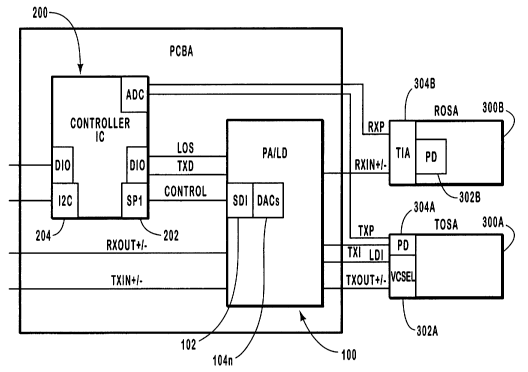
With reference first to Figure l, details are provided concerning various
aspects of
the general architecture of an exemplary embodiment of an integrated post-
amplifier and
laser driver ("PA/LD") assembly 100. Generally, the PA/LD 100 is configured
for
communication with a digital IC controller 200, as well as with a 'transmit'
optical
subassembly ("TOSA") 300A and a 'receive' optical subassembly ("ROSA") 300B.
Among other things, the PA/LD 100 comprises a digital control interface 102,
exemplarily embodied as a serial digital interface, connected with glue logic
module 103
that, in turn, is configured for communication with one or more digital-to-
analog
1o converters ("DAC") 104n. As indicated below in connection with the
discussion of
programmable transceivers and related devices, such DACs comprise an exemplary
implementation of a means for setting a signal parameter in response to signal
parameter
programming instructions, wherein such instructions may, for example, be
received
directly from a user by way of a suitable bus, or may be generated by an
internally coded
algorithm. The scope of the invention is not limited to DACs however. Rather,
any other
system, component or device of comparable functionality may likewise be
employed.
For example, at least some signal parameters may be alternatively be set
through the use
of field programmable gate arrays ("FPGA"s), or similar devices.
One useful aspect of the aforementioned digital control interface is that it
enables
2o the use of multiple control parameters that can be readily multiplexed into
one, or a
relatively small number of, digital control signals. Thus, the digital control
interface
permits a relative increase in the number of PA/LD 100 operations that can be
controlled,
without necessitating a corresponding increase in components or circuitry and,
by virtue
of the use of digital control signals, the digital control interface also
contributes to a
relative decrease in the number of the control signals that are required to
control PA/LD
100 operations. With respect to the foregoing, an internal serial bus
arrangement may
alternatively be employed to implement some or all of the functionality
disclosed herein.
It should be noted here that the PA/LD 100 may be referred to herein as
comprising a 'post-amplifier' or 'post-amplifier assembly,' and a 'laser
driver' or 'laser
3o driver assembly,' exemplary embodiments of which may comprise one or more
amplifiers or other control devices intended to implement certain effects with
respect to
signals transmitted and/or received by the PA/LD 100. In yet other instances,
no
distinction between the post-amplifier and laser driver is made, and the PA/LD
100 may
CA 02494614 2005-02-02
WO 2004/013991 PCT/US2003/024002
7
simply be referred to as comprising various control, and other, devices
intended to
implement certain effects with respect to signals transmitted and/or received
by the
PA/LD 100.
In general however, the devices and/or systems that are concerned with
implementation of functionality that relates primarily to a data signal
received by the
PA/LD 100 are typically referred to as a 'post amplifier' or 'post amplifier
assembly.'
On the other hand, devices and/or systems that are concerned with
implementation of
functionality that relates primarily to control, by the PA/LD 100, of the
transmission of a
data signal are typically referred to as a 'laser driver or 'laser driver
assembly.'
Nonetheless, a device or system that comprises a portion of the 'post
amplifier' in one
embodiment, may comprise a portion of the 'laser driver' in another
embodiment.
Accordingly, the foregoing distinctions are not intended to, nor should be
construed to,
limit the scope of the invention in any way.
In general, the functionality of the integrated post-amplifier and laser
driver
assembly 100 is typically implemented as a single IC on a single-sided PCB. In
some
instances, the PA/LD is implemented as a non-hermetic plastic packaged IC with
lead
frame. However, other types of IC packages, such as ceramic packages, may
alternatively be employed, consistent with the requirements of a particular
application or
operating environment.
2o One useful aspect of the single IC configuration is that it minimizes the
number of
external devices that are required, as some or all of the external devices can
be
incorporated within the IC. By way of example, at least some embodiments of
the
invention obviate the need for external passive devices that perform functions
such as,
but not limited to, set point, matching, filter, and A/C coupling. A related
aspect of the
single IC configuration is that it generally eliminates the need for
connectors, such as flex
connectors, between the post-amplifier and laser driver. Further, the single
IC package
can be incorporated into a relatively small size, as small as 4mm x 4mm in
some cases.
In the illustrated embodiment, the TOSA 300A exemplarily comprises a vertical
cavity surface emitting laser ("VCSEL") 302A in communication with a
photodiode
304A. In at least some embodiments, the VCSEL comprises a non-hermetic lead
frame
plastic package. One aspect of VCSELs that makes them desirable in at least
some
applications is their relatively low cost. Of course, other types of optical
transmitters
CA 02494614 2005-02-02
WO 2004/013991 PCT/US2003/024002
8
may also be employed. In general, any light transmission source, and
transmission
wavelength, that is compatible with PA/LD 100 may be used.
Similarly, ROSA 300B exemplarily comprises a PIN photodiode 302B in
communication with a transimpedance amplifier ("TIA") 304B and, in this
embodiment
at least, requires no capacitors for its operation. Moreover, in at least some
embodiments, the ROSA is implemented as a non-hermetic lead frame plastic
package.
As in the case of the TOSA 300A however, other embodiments of ROSA 300B may
alternatively be employed.
In some embodiments, one or both of the TOSA 300A and ROSA 300B further
io include systems and/or devices to aid in evaluation and diagnostic
evolutions concerning
their performance and/or the performance of related components and systems. By
way of
example, the TOSA 300A and/or ROSA 300B in such embodiments includes a log
amplifier for use in conjunction with a monitor photodiode, such as PIN
photodiode
302B or photodiode 304A, and/or current mirror circuitry.
Another aspect of some embodiments of the TOSA 300A is that they provide for
a DC active bias for laser modulation. This eliminates the need for bias T
modulation
devices and circuitry such as are typically employed in laser modulation
applications.
With continuing reference now to aspects of the exemplary PA/LD illustrated in
Figure 1, exemplary embodiments of the PA/LD 100 are configured to transmit,
receive,
2o and/or process a variety of different signals. Such signals may comprise,
among other
things, data and monitoring signals, control signals, or may be concerned with
the
transmission of power to/from various components. In this exemplary
embodiment, the
data signals are digital and include those signals designated RXIN+/- and
RXOUT+/
and which denote, respectively, a data signal received from ROSA 300B, and a
data
signal transmitted by the PA/LD 100 to a customer. Similarly, the signals
designated
TXIN+/- and TROUT+/- denote, respectively, a data signal received by the PA/LD
100
from a customer, and a customer data signal transmitted to TOSA 300A. In any
case, the
+/- designation refers to the fact that, in at least some embodiments, the
signal channel
consists of two data transmission lines of opposite polarities. Thus, in this
exemplary
3o implementation, the signal designated TXIN+/- actually comprises a first
line TX1N+
and a second line TXIN-.
Note that, as suggested by the foregoing, the RXIN+/- and RXOUT+/- typically
do not comprise discrete signals. Rather, the RXOUT+/- signal simply comprises
a
CA 02494614 2005-02-02
WO 2004/013991 PCT/US2003/024002
9
version of the RXIN+/- signal that has been modified, such as by way of
changes to
parameters such as its polarity, rise time, or amplitude, for example. The
same is
likewise true with respect to the TXIN+/- signal and the TROUT+/- signal.
With continuing reference now to Figure 1, PA/LD 100 is also configured to
receive, via the digital control interface 202 of the digital IC controller
200, various
control signals pertaining to the operation of the TOSA 300A and/or to the
processing of
the RXIN+/- data signal received by PA/LD 100 from ROSA 300B. Such control
signals can be tailored according to any of a variety of variables. For
example, the
temperature of VCSEL 302A may be used as a basis for modifications or
adjustments to
l0 a control signal relating, for example, to a bias point for a circuit
element of PA/LD 100.
Examples of such control signals are considered in further detail below.
Yet another exemplary control signal transmitted from the digital IC
controller
200 to the PA/LD 100 is the TXD signal. In general, the TXD signal directs the
PA/LD
100 to shut down the TOSA 300B. Shutdown of the TOSA 300B may be implemented,
for example, when it is desired to power down a module to facilitate
performance of
diagnostics, or when there is a fault indication such as an internal short or
excessive
transmit power. As indicated in Figure 1, the TXD signal may, in at least some
cases, be
transmitted from the digital IC controller 200 to the PA/LD 100 other than by
way of the
respective digital control interfaces of those components. Note that the same
is likewise
true with respect to the LOS signal for example, as discussed below.
In addition to the various control signals generated and transmitted to the
PA/LD
100 by the digital IC controller 200, signals generated by one of the optical
devices may
likewise be used to aid in the control of those devices and/or for other
purposes. By way
of example, in the embodiment of PA/LD 100 illustrated in Figures 1 and 2, the
TOSA
300A generates the TXI signal and transmits the TXI signal to the PA/LD 100.
In
general, the TXI signal received at the PA/LD 100 from the TOSA 300A indicates
the
level of current at which the TOSA 300A is operating. In this exemplary
embodiment,
the TXI signal serves as an input to a power supply circuit of the PA/LD 100
that is used
to control the input voltage to the VCSEL (Figure 1 ), as discussed in further
detail below.
Note that in some cases, the TXI signal may be used for purposes other than
implementing a control functionality. By way of example, some exemplary
embodiments
use the TXI signal to implement a monitoring functionality with respect to the
VCSEL
CA 02494614 2005-02-02
WO 2004/013991 PCT/US2003/024002
302 current. Details concerning one such exemplary embodiment are provided
below in
conjunction with the discussion of the TXP signal.
As suggested earlier, embodiments of the PA/LD 100 are also configured to
transmit, receive, and/or process a variety of monitoring signals pertaining
to the
5 operation and/or status of various components. One example of a monitoring
functionality implemented by way of the PA/LD 100 is indicated by the LOS
signal.
Generally, the LOS signal is generated and transmitted by the PA/LD 100 to the
digital
IC controller 200 when the incoming data signal RXIN+/- has been lost, or
otherwise
fails to comport with certain established criteria.
to Other exemplary monitoring functionalities related to, but not necessarily
implemented by this exemplary embodiment of, the PA/LD 100, include the TXP
signal
transmitted from the TOSA 300A to the digital IC controller 200 indicating the
optical
power of the TOSA 300A. More particularly, the TXP is an electrical signal
that is
proportional to the optical power in the VCSEL 302A. A similar monitoring
signal is
generated with respect to the operation of the ROSA 300B. In particular, the
RXP signal
transmitted from the ROSA 300B to the digital IC controller 200 indicates the
optical
power of the ROSA 300B. Exemplarily, the RXP signal comprises an electrical
signal
that is proportional to the optical power in the ROSA 300B photodiode 302B.
Some of the monitoring signals, such as the TXP signal for example, may be
used
for purposes other than implementing a monitoring functionality. By way of
example,
some exemplary embodiments use the TXP signal as an input to a power supply
circuit
that is used to control the power input to the TOSA 300A.
In connection with the foregoing discussion of exemplary aspects of the TXP
and
TXI signals, it should be noted that the functionality of the TXP and TXI
signals and,
more generally, other signals disclosed herein, may be interchanged in some
cases if
necessary to suit the requirements of a particular application.
As noted earlier, the implementation of the PA/LD 100 illustrated in Figures 1
and 2 is configured so that the TXP signal provides a monitoring functionality
with
respect to TOSA 300A performance, and the TXI signal serves as the input to a
power
3o supply circuit that controls the power to the TOSA 300A. Alternatively
however, other
implementations of the PA/LD 100 may be configured so that the TXI signal
provides the
monitoring functionality with respect to TOSA 300A performance, while the TXP
signal
serves as the input to the power supply circuit that controls the power to the
TOSA 300A.
CA 02494614 2005-02-02
WO 2004/013991 PCT/US2003/024002
11
In either case, the monitoring signal may be provided to internal and/or
external users. In
yet other implementations of the PA/LD 100, the signal that provides the
monitoring
functionality may be omitted altogether. Thus, the foregoing are exemplary
implementations and are not intended to limit the scope of the invention in
any way.
In addition to the signals that implement various monitoring and control
functionalities, yet other signals employed in conjunction with the PAILD 100
concern
aspects of PA/LD 100 operations such as power transmission and control. By way
of
example, the LDI signal is the actual DC bias current that is applied to the
TOSA 300A
to power the VCSEL 302A. As another example, the reference voltage signal VREF
is
1o an input to a feedback system that controls the input voltage to the VCSEL.
Of course, the enumeration and combinations of the various data, monitoring,
power, control, and other, signals disclosed herein are exemplary only and are
not
intended to limit the scope of the invention. Accordingly, other exemplary
embodiments
of PA/LD 100 may include, implement or embody additional or alternative
functionalities, as necessary to suit the requirements of a particular system
or application.
Moreover, feedback loops and circuits may be employed in connection with a
variety of
different signals, and combinations thereof, in the monitoring andlor
controlling of the
performance of various systems and devices. Thus, the scope of the invention
should not
be construed to be limited to the exemplary embodiments disclosed herein.
Directing attention now to Figure 2, further details are provided concerning
various aspects of the architecture of an exemplary embodiment of the PA/LD
100. As
indicated there, the digital control interface 102 of this embodiment of the
PA/LD 100
exemplarily comprises a three pin configuration adapted to receive master-in-
slave-out
("MISO") and master-out-slave-in ("MOSI") control signals at 'data' and
'enable' pins,
respectively, as well as a system clock ("SCK") signal, from the digital IC
controller 200.
While two and three pin serial interfaces are particularly useful in some
embodiments of
the invention, the serial interface may, more generally, be implemented as any
industry
standard, or customized, serial interface.
The digital control interface 102 communicates, in turn, with a plurality of
DACs
104A through 104n by way of glue logic module 103. In the illustrated
embodiment,
nine DACs are provided, although the number may vary depending upon the
requirements of a particular application or system. As discussed below, the
DACs
generally operate to convert a digital control signal into an analog signal
that can be acted
CA 02494614 2005-02-02
WO 2004/013991 PCT/US2003/024002
12
upon by the PA/LD 100. In this exemplary embodiment, some of the DACs comprise
8
bit DACs, but various other types of DACs may alternatively be employed.
As indicated in Figure 2, the DACs in this exemplary embodiment are concerned
with, respectively, the following signals: DAC 104A - RXRT (control transition
time of
RXIN+/-); DAC 104B - RXAMP (control amplitude of RXIN+/-); DAC 104C -
LOSHYST (loss of signal hysteresis for RXIN+); DAC 104D - LOSTH (loss of
signal
threshold for RX1N-); DAC 104E - TXRT (control transition time of TROUT+/-);
DAC
104F - TRAMP (control amplitude of TROUT+/-). In addition to the foregoing, a
DAC
1046 is provided that communicates with a power supply circuit 106 to control
power
input LDI to TOSA 300A by way of a reference voltage signal VREF. Further, DAC
104H and DAC 104I are provided that are generally concerned with,
respectively,
controlling the polarity of TROUT+/- and RXOUT+/-. In some implementations, a
feedback loop or circuit is provided that provides information concerning LDI.
With continuing reference to Figure 2, various amplifiers, which exemplarily
comprise radio frequency ("RF") amplifiers, are provided that communicate with
respective DACs and generally act to implement certain actions specified by
the control
signal received by the PA/LD 100 from the digital IC controller 200. For
example, the
illustrated embodiment of PA/LD 100 includes an RX amplifier 108 that receives
analog
input from DACs 104A,104B and 104I and modifies RXIN+/-, in accordance with
such
2o inputs, to produce RXOUT+/-. In the illustrated embodiment, RX amplifier
108 is
configured to modify the transition time, amplitude and polarity of RXIN+/-.
Further, the RX amplifier 108 is exemplarily configured with CZ+/-ports for
use
in bypassing a feedback network, such as may be used to bias the RX amplifier
108. In
this exemplary arrangement, a large, external capacitor placed between the
CZ+/-ports.
In other embodiments however, such biasing is achieved without the need for
the external
capacitor, and hence the CZ+/- ports.
Additionally, an LOS circuit 110, exemplarily embodied as an amplifier, is
provided that monitors RXIN+/- and transmits an LOS signal to the digital IC
controller
200 when RXIN+/- exceeds, or falls below, a predefined threshold. Also, the
LOS
3o circuit 110 implements a hysteresis functionality to minimize or eliminate
random
switching of the LOS signal, usually caused by small variations in received
signal
strength or noise and often referred to as 'chatter,' that would likely
otherwise result as
RXIN+/- moves back and forth over the predefined threshold.
CA 02494614 2005-02-02
WO 2004/013991 PCT/US2003/024002
13
The illustrated embodiment of the PA/LD 100 further includes a TX amplifier
112 that receives analog input from DACs 104E, 104F and 104H and modifies
TXIN+/-,
in accordance with such inputs, to produce TROUT+/-. In the illustrated
embodiment,
the TX amplifier 112 is configured to modify the transition time, amplitude
and polarity
of TX1N+/-. In at some embodiments, the TX amplifier 112 may be implemented as
a
plurality of amplifiers, each of which is concerned with the control of one of
the
transition time, amplitude and polarity of the TXIN+/- signal. In yet other
embodiments,
the TX amplifier 112 may be implemented as a single mufti-stage amplifier so
that all of
the aforementioned control functionalities concerning the TXIN+/- signal are
1o implemented by a single component. Note that the foregoing discussion is
equally
germane to the RX amplifier 108.
While the aforementioned exemplary embodiments are concerned with, among
other things, control of data signal polarity, it may be useful in some
instances to be able
to control the polarity of other signals as well. By way of example, some
embodiments
additionally, or alternatively, provide for the control of the polarity of the
LOS and TXD
signals. As suggested by the foregoing example then, embodiments of the
invention
should not be construed to be limited to polarity control as applied to data
signals.
Finally, it should be noted that signal polarity control may also be
implemented
with respect to analog data or other signals, as controlled by analog control
signals. In
2o exemplary implementations of this type, a digital control interface is not
required, and a
suitable analog control interface may be employed instead.
Directing attention now to Figure 3, further details are provided concerning a
control device, exemplarily embodied as RX amplifier 108 and TX amplifier 112,
for
controlling the polarity of a data signal. As suggested in Figure 3, the same
general
configuration may be employed for RX amplifier 108 and TX amplifier 112.
However,
the components used to implement such configurations may vary depending on
whether
the RX amplifier 108 or the TX amplifier 112 is implemented. For example, in
the case
of the RX amplifier 1 O8, a relatively larger number of gain stages may be
employed since
a relatively larger gain may be required. In the case of the TX amplifier 112
on the other
3o hand, relatively large high-current transistors may be employed as
necessary for the TX
amplifier 112 to drive the required current to the load.
Exemplarily, the TX amplifier 108 includes a polarity inverter 108A, as well
as
two output stages 108B and 108C. Similarly, RX amplifier 112 includes a
polarity
CA 02494614 2005-02-02
WO 2004/013991 PCT/US2003/024002
14
inverter 112A and two output stages 112B and 112C. At least some embodiments
of the
TX amplifier 108, as well as the RX amplifier 112, further include an input
stage (not
shown) as well and may include additional output stages. The foregoing
amplifier
configurations are exemplary only however. In this regard, it was noted
earlier herein
that some embodiments of the invention may use multiple single-stage
amplifiers instead
of the multi-stage amplifier illustrated in Figure 3. In general then, any
amplifier or
control device configuration useful in implementing the functionality
disclosed herein
may be employed.
The illustrated embodiments of TX amplifier 108 and RX amplifier 112 are each
1o configured with three control inputs, though various other control inputs
and
combinations thereof may be employed. As discussed earlier, the TX amplifier
108 is
configured to receive the TXPOL signal at the polarity inverter 108A, and to
receive the
TXRT and TXAMP signals at the 108B output stage and 1080 output stage,
respectively.
Similarly, the 1ZX amplifier 112 is configured to receive the RXPOL signal at
the polarity
inverter 112A, and to receive the RXRST and RXAMP signals at the 112B output
stage
and 112C output stage, respectively.
As discussed in greater detail below, the TX amplifier 108 uses the TXPOL,
TXRT and TXAMP signals to generate an output signal TXOUT+/- having desired
characteristics. Likewise, the RX amplifier 112 uses the RXPOL, RXRST and
RXAMP
2o signals to generated an output signal RXOUT+/- having desired
characteristics.
It should be noted here that the various types and combinations of amplifiers,
as
well as their respective functionalities, disclosed herein are exemplary only.
Various
other types of control systems and devices may alternatively employed. In
connection
with the foregoing, the combinations of functionalities implemented by way of
PA/LD
100 are, likewise, exemplary only and are not intended to limit the scope of
the invention
in any way. Accordingly, additional or alternative fiznctionalities, and
combinations
thereof, may also be implemented by PA/LD 100, as necessitated by the
requirements of
a particular system or application.
C. General Aspects of PAJLD Operations
3o With continuing attention to Figures 1 through 3, and directing attention
now to
Figures 4 through 6, details are provided now concerning certain operational
aspects of
the illustrated embodiment of PA/LD 100 and various related components. With
CA 02494614 2005-02-02
WO 2004/013991 PCT/US2003/024002
attention first to Figure 4, aspects of an exemplary method 400 for receiving
and
processing an incoming control signal are illustrated.
In particular, at state 402, the control signal initially transmitted from the
digital
IC controller 200 is received at the PA/LD 100. Exemplarily, such signals
relate to,
5 among other things, the processing of TXIN+/- and RXIN+/-, the operation of
TOSA
300A, and the disablement of PA/LD 100. Some of the control signals
transmitted by the
digital IC controller 200 may be received at the digital control interface 102
of PA/LD
100, while other control signals transmitted by the digital IC controller 200,
such as the
TXD signal, are received directly at the 'glue logic' module 103. This
arrangement is
1o exemplary only however, and various alternative schemes for receipt of
incoming control
signals at the PA/LD 100 may be implemented.
In general, the control signals transmitted by the digital IC controller 200
and
received at the PA/LD 100 comprise one or more digital words, comprised of a
defined
sequence of digital bits, which may constitute instructions and/or parameter
values.
15 When the control signal has been received at PA/LD 100, state 404 is
entered wherein the
glue logic module 103 parses the control signal and directs the digital words,
or portions
thereof, into the various discrete instructions and/or parameter values.
After parsing has been completed, state 406 is entered. At this state, the
glue
logic module 103 directs the parsed segments of the data signal to the
appropriate
2o registers within the glue logic module. Because each register corresponds
with a
particular DAC, the parsed segments of the data signal can thus be stored in a
manner
consistent with the way in which the particular segment is to be employed. By
way of
example, a parsed segment of the control signal that concerns the threshold
for the LOS
signal is stored in a DAC that is configured to communicate with the LOS
circuit 110.
At such time as the incoming control signal has been parsed and registered,
the
PA/LD 100 then performs various actions based upon the parsed instructions
and/or
values. Thus, control information concerning a wide variety of PA/LD 100
operations
can be transmitted by way of a single control signal. Moreover, the control
signal
requires only a single digital interface at the PA/LD 100. This arrangement
considerably
3o simplifies the physical implementation of the PA/LD 100, as well as the
processing of the
incoming control signal.
Directing attention now to Figure 5, details are provided concerning aspects
of an
exemplary process 500 for implementing actions based upon one or more control
signals.
CA 02494614 2005-02-02
WO 2004/013991 PCT/US2003/024002
16
As discussed below, Figure 5 depicts only certain general aspects of such an
exemplary
process, and reference to more particular implementations is made after
aspects of the
process illustrated in Figure 5 have been addressed.
In general, state 502 is entered wherein the glue logic module 103 accesses
and
retrieves the instructions and/or values stored in the various registers.
Next, state 504 is
entered wherein the applicable DACs convert the accessed instructions and/or
values
from digital to analog form. After this conversion has been completed, state
506 is
entered and the applicable DACs generate and transmit corresponding analog
signals to
the appropriate amplifiers. In state 508, the appropriate amplifiers receive
the analog
l0 signals and then move to state 510 where various actions are implemented
with regard to
the signals with which such amplifiers are concerned.
D. Asuects of Exemplary PA/LD Ouerations - TX Amplifier & TOSA
With more particular reference now to the input customer data signal TXIN+/-
(Figure 2), DACs 104E, 104F and 1046, respectively, convert the words, or
portions
thereof, relating to the TXIN+/- transition time, TXIN+/- amplitude and TXIN+/
polarity, to an analog form and then transmit the analog signals TXRT, TRAMP
and
TXPOL, as/if applicable, to TX amplifier 112.
In response, the TX amplifier 112 then adjusts the transition time, amplitude
and/or polarity of TXIN+/- consistent with the TXRT, TRAMP and TXPOL signals,
respectively, as necessary to convert signal TX1N+/- into a signal TROUT+/-
that is
suitable for driving the VCSEL 302. The TROUT+/- signal is then transmitted by
the
PA/LD 100 to VCSEL 302A of TOSA 300B. Of course, this operational scenario
concerning the use of the combination of the TXRT, TRAMP and TXPOL signals is
exemplary only and various other parameters of TXIN+/-, and combinations
thereof,
may be monitored and/or controlled as well.
With continuing attention to Figures 1 and 2, details are provided concerning
exemplary operational aspects of the TOSA 300A. In the illustrated embodiment,
the
TOSA 300A receives the TROUT+/- signal and the VCSEL 302A then transmits an
optical signal (not shown) consistent with the received TROUT+/-. In this way,
the
3o performance of VCSEL 302A can be adjusted and controlled in response to
variables
such as, but not limited to, temperature and voltage, so as to achieve
transmission of an
optical signal having certain desired properties or characteristics.
CA 02494614 2005-02-02
WO 2004/013991 PCT/US2003/024002
17
At substantially the same time as the VCSEL 302A transmits the optical signal,
the photodiode 304A receives at least a portion of the optical signal
transmitted by
VCSEL 302A. Finally, the photodiode 304A generates and transmits the TXP
signal to
the digital IC controller 200, thereby indicating the optical power of the
TOSA 300A. In
this exemplary implementation, the TXP signal primarily serves to facilitate a
monitoring
functionality with respect to TOSA 300A performance. In addition to the TXP
signal,
the photodiode 304A also generates and transmits the TXI signal. As discussed
in further
detail below, the TXI signal is employed, in this exemplary embodiment, to
facilitate
control of TOSA 300A operations by way of power supply circuit 106.
1o In general, the power supply circuit 106 uses the TXI signal, in
conjunction with
the VREF signal, to vary, as necessary, the input current to the VCSEL 302A.
As
discussed earlier, the TXI is generated by the TOSA 300A and indicates the
level of
current at which the TOSA 300A is operating. On the other hand, the VREF
signal
represents a desired VCSEL 302A bias point. Typically, the value of the VREF
signal,
15 expressed as a signal reference voltage, is specified by digital IC
controller 200 and
transmitted to the PA/LD 100 as part of a control signal. The glue logic
module 103
cooperates with DAC 1046 to cause the generation and transmission of the VREF
signal
to the power supply circuit 106.
Thus, in the event that the feedback voltage from the TOSA 300A, indicated by
or
20, derived from the TXI signal, does not match the VREF signal reference
voltage, then the
power supply circuit 106 adjusts the LDI input to the TOSA 300A until a match
is
achieved. Thus, the power supply circuit 106 uses the feedback provided in the
form of
the TXI signal, in conjunction with the predetermined reference voltage
provided in the
form of the VREF signal, to determine and adjust, if necessary, the input
power LDI to
25 the VCSEL 302A and, thus, the optical power of the TOSA 300A. As noted
earlier, the
TXP signal may be employed in place of the TXI signal to provide similar
control
functionality with respect to TOSA 300A.
As an alternative to controlling various aspects of the TOSA 300A operations,
it
may be desirable in some instances to suspend the operation of TOSA 300A. To
that
30 end, the TXD signal is generated and transmitted by digital IC controller
200 to PA/LD
100 upon the satisfaction of certain conditions, andlor the occurrence of
certain events,
relating to the system. For example, the TXD signal would be generated and
transmitted
in the event of the occurrence of a predefined fault condition. In cases where
the TXD
CA 02494614 2005-02-02
WO 2004/013991 PCT/US2003/024002
18
signal has been generated and transmitted, the PA/LD 100 responds to the TXD
signal by
terminating transmission of the LDI signal to TOSA 300A, and thus data
transmission by
TOSA 300A, upon receipt of the TXD signal. Data transmission is then
recommenced
upon receipt, by the PA/LD 100, of an appropriate signal by way of the
'enable' pin of
the digital control interface 102.
E. Asuects of Exemplary PA/LD Ouerations-RX and LOS Amplifiers
& ROSA
It should be noted here that certain general aspects of an exemplary process
500
for using control devices such as amplifiers to implement actions concerning
various
optical devices, based upon one or more control signals received from a
digital IC
controller or other source, have already been discussed above in connection
with Figure
5. Accordingly, the following discussion will focus primarily on certain
exemplary
implementations of process 500 as they relate to the operation of the RX
amplifier 108,
the LOS circuit 110 and/or the ROSA 3OOB.
With respect first to the ROSA 300B, it was noted earlier that ROSA 300B
converts an optical input signal, received at photodiode 302B, into the
electrical signal
RXIN+/- which is then received by the PA/LD 100. In general, the PA/LD 100
controls
various aspects of the RXIN+/- signal, in accordance with a control signal
received from
the digital IC controller 200. The modified RXIN+/- signal is then transmitted
by the
2o PA/LD 100 to the customer as the RXOUT+/- signal.
Aspects of an exemplary process for performing various operations concerning
the RXIN+/- signal generated by the ROSA 300B will now be considered in
further
detail. In particular, DACs 104A, 104B and 104I, respectively, convert the
words, or
portions thereof, of the control signal relating to the RXIN+/- transition
time, RXIN+/-
amplitude and RXIN+/-polarity, to an analog form and then transmit the analog
signals
RXRT, RXAMP and/or RXPOL, to RX amplifier 108. The RX amplifier 108 then
adjusts, if necessary, the transition times amplitude and/or polarity of
RXIN+/- consistent
with the received RXRT, RXAMP and/or RXPOL signals, respectively. The modified
RXIN+/-, denoted as output signal RXOUT+/-, is then transmitted by the PA/LD
100 to
the customer. It should be noted that the foregoing operational scenario
concerning
processes relating to the RXIN+/- signal is exemplary only and various other
parameters
of RXIN+/- may be monitored and/or controlled as well.
CA 02494614 2005-02-02
WO 2004/013991 PCT/US2003/024002
19
In addition to the RX1N+/- signal discussed above, ROSA 300B also generates
the RXP signal which provides feedback to digital IC controller 200 concerning
the
optical power of photodiode 302B. In general, signals concerning ROSA 300B
performance, and/or the performance of TOSA 300A, such as the RXP, TXP and TXI
signals, may be generated and transmitted substantially continuously, or on
any other
desired basis.
In addition to controlling various parameters of RXIN+/-, some embodiments of
PA/LD 100 are also configured to monitor, and report on, aspects of the status
of
RXIN+/-. In one exemplary embodiment, DACs 104C and 104D convert the
hysteresis
and threshold data, received from digital IC controller 200 as words or
portions thereof,
to an analog form and then transmit, respectively, the LOSHYST and LOSTH
signals to
the LOS circuit 110. The LOS circuit 110 then monitors RXIN+/-and transmits
the LOS
signal to the digital IC controller 200 when RXIN+/- exceeds, or falls below,
a
predefined threshold, and/or when no data is detected in the RXIN+/- signal.
Finally, the LOS circuit 110 also implements a hysteresis functionality to
minimize or eliminate chatter on the LOS signal that may otherwise result as
RXIN+/-
moves back and forth over the predefined threshold. In particular, in the
event that
RXIN+/- moves below the predefined threshold, it must drop substantially below
that
threshold before the LOS signal will be generated and transmitted. The same is
likewise
2o true in the case where RXIN+/-moves above the predefined threshold. The
upper and/or
lower thresholds may be defined as necessary to suit the requirements of a
particular
application. In some embodiments of the invention, such loss of signal
functionality may
also be implemented with respect to the customer signal RXIN+/-.
F. Aspects of Exemplary Signal Polarity Control - RX and TX
Amplifiers
As noted earlier, the functionality implemented by the RX amplifier 108 and
the
TX amplifier 112 includes, among other things, controlling the polarity of the
output data
signals RXOUT+/- and TROUT+/-, respectively.
Accordingly, one aspect of the data signal polarity control functionality
provided
by embodiments of the invention is that it allows for a relatively higher
degree of
flexibility in terms of the layout and implementation of the components that
comprise the
PA/LD 100 and related systems. In particular, because the polarity of data
signals
received at the PA/LD 100 can be readily modified, prior to further
transmission, in
CA 02494614 2005-02-02
WO 2004/013991 PCT/US2003/024002
response to a control signal, it is of little consequence that a data signal
entering the
PA/LD is improperly polarized, since the polarity can be corrected before the
PA/LD 100
transmits the data signal on to the next user.
Moreover, the use of a digital control interface also enhances the ease with
which
5 data signal polarity control can be implemented. In particular, the digital
control
interface is adapted for use with data, representing multiple control
parameters, that have
been multiplexed into one, or a few, control signals. Thus, signal polarity
control can be
implemented easily and without compromising the number and type of other
control
parameters that can be multiplexed into the control signal.
1 o Control of such output data signal polarity may be accomplished in various
ways.
Some exemplary implementations are addressed below, however, other processes
and
methods may alternatively be employed.
With reference to use of the TXPOL signal for example, the polarity of the
output
data signal TROUT+/- is changed by electronically crossing-over the TXIN+ and
TXIN-
15 propagation paths, which causes the TXOUT+ signal to propagate along the
path along
which the TROUT- signal would otherwise have propagated, and vice-versa. The
foregoing polarization adjustment scheme is likewise germane to data signal
polarity
adjustments made by the RX amplifier 10~ to RXOUT+/- in response to the RXPOL
signal.
20 In another case, the signal inversion can be accomplished by reprogramming
a
positive gain block to be a negative gain block, or vice versa. As another
example, the
data path can be programmed to pass through either a positive gain block or
through a
negative gain block. More generally however, any device and/or process, or
combination
thereof, that is effective in modifying and/or maintaining, as applicable, the
relationship
between the data paths so that the appropriate significance can be assigned to
the detected
differential between the two paths, may be employed.
As suggested by the foregoing, a variety of means may be employed to perform
the functions disclosed herein, of an amplifier or other control device. Thus,
the
embodiments of the amplifiers disclosed herein are but exemplary structural
3o implementations of a means for controlling signal polarity and, as such,
those exemplary
implementations should not be construed as limiting the scope of the present
invention in
any way. Rather, any other structure or combination of structures effective in
implementing the functionality disclosed herein may likewise be employed.
CA 02494614 2005-02-02
WO 2004/013991 PCT/US2003/024002
21
G. General Aspects of a Programmable Transceiver
As discussed above, it is useful to be able to control various aspects of the
operation of the PA/LD and, more broadly, the associated transceiver, in order
to
accommodate changes in environmental and operating conditions, and to enhance
the
overall operational flexibility of the associated transceiver, systems, and
devices.
Accordingly, at least some embodiments of the invention are configured to
enable ready
implementation of changes concerning aspects of their performance and
operation.
More particularly, exemplary embodiments of the invention are directed to
programmable transceivers and other devices that are configured to enable a
user to
to program, and reprogram, the transceiver or device such that the transceiver
or device
operates in a desired manner. As discussed in further detail below, references
herein to
'programmable' devices refers generally to the capability of such devices to
receive,
store, process, execute and/or modify signal parameter programming
instructions.
Exemplary embodiments of the invention are additionally, or alternatively,
configured so
that the adjustments to the performance and operation of the transceiver or
device can be
performed "on-the-fly" while the transceiver or device is in an operating
mode.
Implementation of one or both of the aforementioned functionalities, in
connection with the feedback and control aspects discussed earlier herein,
means that
exemplary embodiments of the transceiver are able to readily accommodate a
dynamic
operating environment, as exemplified by changes in protocols, line rate
variations,
changes in operating requirements and operating conditions, and other
considerations that
relate to or implicate in some way the operation and performance of the
transceiver.
With further general reference to the aforementioned feedback and control
aspects,
exemplary embodiments of the invention are configured with feedback systems to
ensure
that the performance of a particular system, device, or component remains
within a
defined range, notwithstanding that the defined range can be readily
reprogrammed.
Attention is now directed to various general aspects of an exemplary
implementation of a programmable transceiver. As suggested above, the
transceiver can
be programmed at various times, and in various ways, to achieve certain
operational and
performance results. For example, it is often useful to specify and/or modify,
through
suitable programming, various parameters of signals asserted and/or de-
asserted by, or in
connection with, the PA/LD, where such signals include, but are not limited
to, data,
monitoring, power, and control signals.
CA 02494614 2005-02-02
WO 2004/013991 PCT/US2003/024002
22
The signal parameters that can be programmed in connection with
implementations of the invention are virtually unlimited. Examples of
programmable
signal parameters include, but are not limited to, signal rise time, signal
polarity, signal
amplitude, and signal fall time. Other aspects concerning signals, such as
signal assertion
and de-assertion thresholds (sometimes also referred to as signal "trip
levels") may be
programmed as well.
As suggested by the foregoing, exemplary embodiments of the invention are
concerned both with the programming of various characteristics of the actual
signal, such
as polarity and amplitude for example, as well as with the programming of
aspects of the
l0 signal that, while not comprising a characteristic specific to a signal,
nonetheless relate to
the signal in some way, such as assertion and de-assertion thresholds of a
signal. Such
signal characteristics and signal aspects may be referred to collectively
herein as "signal
parameters."
Various factors may influence the need to program and/or reprogram one or more
signal parameters. By way of example, a change in the line rate of the system
in
connection with which the transceiver is employed, such as from a 2 gigabits
rate to a 10
gigabits rate, implicates a change in the level of power that is incident on
the optical
receiver of the transceiver. In this example, such a change in incident power,
accordingly
necessitates, among other things, reprogramming of the LOS assert and de-
assert
2o thresholds. These changes would also be necessitated where, for example, it
is desired to
remove the transceiver from a system having a first line rate, and install the
transceiver in
a system having a second, different, line rate.
Other factors may likewise necessitate the reprogramming of one or more signal
parameters. For example, a system protocol change, such as may occur when a
system is
upgraded, or when the transceiver is removed from one system and installed in
another,
would require changes to any number of signal parameters.
In similar fashion, environmental conditions may play a significant role in
determining whether or not reprogramming of signal parameters is required. For
example, changes in the operating temperature of the system and/or transceiver
often
3o implicate a need to reprogram the rise and fall times of certain signals.
With reference to one particular example, it is sometimes desirable to provide
for
thermally-based correction of a VHF input to a power supply circuit (see
Figures 1 and
2). In some implementations, such corrections are performed in connection with
input
CA 02494614 2005-02-02
WO 2004/013991 PCT/US2003/024002
23
received from an appropriate temperature sensor associated with the
transceiver. In this
example, a particular VHF is programmed that causes an increase in the power
transmitted to the TOSA 300A when the temperature of the system, TOSA 300A, or
other elements, components or devices falls within a predefined temperature
band.
It should be noted that the foregoing is not intended to be, nor is, an
exhaustive
list of factors that may implicate the programming andlor reprogramming of one
or more
parameters of the signals with which the transceiver, and related systems and
devices, are
concerned. Rather, the aforementioned factors simply serve to exemplify
situations and
conditions that may bear on the desirability and need to program the
transceiver.
l0 As suggested above, one aspect of exemplary embodiments of the invention is
that they permit ready programming and/or reprogramming of the transceiver so
that
various signal parameters can be modified may be necessary to accommodate
factors
such as line rate and protocol changes, as well as environmental factors such
as
temperature. More particularly, exemplary embodiments of the invention are
configured
to enable at least two different programming modes, which may be used
together, or in
the alternative.
In a first programming mode, a user is able to customize the performance and
operation of the transceiver consistent with the requirements of a particular
application or
situation by specifying certain signal parameter values. In the event that
changes to one
or more of such parameters are desired, the user can simply reprogram the
transceiver
accordingly.
A second programming mode that is additionally, or alternatively, employed by
exemplary embodiments of the invention is an "on-the-fly" programming mode
where
one or more signal parameters are changed or adjusted automatically in
response to
changes in system protocols, line rates, operating requirements, operating
conditions, and
other considerations that relate to the operation and performance of the
system or device.
In this programming mode, no user input is required beyond the initial
programming of
the device. In some implementations of this programming mode, relationships
are
established between and among two or more signal parameters so that in the
event that
one parameter is reprogrammed, other parameters may likewise be automatically
reprogrammed, in accordance with the established relationship(s).
Various techniques may be employed in the programming of the transceiver.
With reference to the first programming mode noted above, such programming is
CA 02494614 2005-02-02
WO 2004/013991 PCT/US2003/024002
24
exemplarily implemented, with a suitable processor and software, by way of the
I2C bus
204 and appropriate DACs of the digital IC controller 200 (see Figure 1), but
may be
implemented in other ways as well. In some implementations, the processor
comprises
an element of the transceiver, while in other cases, the processor may be
external to the
transceiver.
As to "on-the-fly," or dynamic, programming, various devices and techniques
may be employed to this end. For example, some exemplary implementations of
the
transceiver are programmed with algorithms that monitor one or more
predeterniined
system characteristics and performance such as, but not limited to,
temperature, line rate
l0 and system protocol, and operate in conjunction with corresponding DACs
and/or other
systems and devices to automatically change predefined parameters of one more
designated signals accordingly. Thus, the DACs may, in various implementations
of the
invention, be programmed, dynamically controlled, or both, as desired to
obtain
particular results. Exemplarily, any such changes in programming are logged
and/or
transmitted to a computer or other monitoring device for tracking and
evaluation by
system operators. Monitoring of the algorithm in this way enables system
operators to
identify changes that may be required to the algorithm.
At least some of the aforementioned algorithms include or employ features such
as lookup tables that are consulted periodically, or on an as-needed basis,
and that
2o provide signal parameter values for implementation by the algorithm. In
some
implementations of the invention, the algorithm operates in connection with
hardware
such as temperature detectors and protocol detector circuits which provide
input to the
algorithm that is then used to make a determination as to whether or not a
signal
parameter change is required. Of course, the foregoing are exemplary
implementations
only, and various other combinations of hardware and software may likewise be
employed in connection with the dynamic control of the transceiver.
H. Exemplary Programmable Signal Parameters
As discussed above, it is desirable to adjust various parameters of signals
with
which the PA/LD and associated transceiver are concerned. The assert and de-
assert
thresholds for the LOS signal generated by the LOS amplifier comprise but one
example
of such a signal parameter. Directing attention once more to Figure 2, and to
Figure 6 as
well, details are provided concerning an exemplary implementation of the
invention that
provides for, among other things, programmable RXIN+/- LOS trip levels. In
general,
CA 02494614 2005-02-02
WO 2004/013991 PCT/US2003/024002
programmable LOS trip levels enable a device to be readily adapted to changing
system
conditions, protocols and line rates while, at the same time, allowing for a
relatively more
narrow range of trip conditions and, thus, a relative improvement in the
sensitivity and
performance of the programmable device.
5 With attention now to Figure 6 in particular, a schematic diagram is
presented that
illustrates various aspects of a device configured to enable programming of
RXIN+/-
LOS thresholds. It should be noted here that, in order to facilitate
discussion, exemplary
embodiments of the digital IC controller 200 and the PA/LD 100 are presented
in Figure
6 in a somewhat simplified form, and further details concerning exemplary
10 implementations of those components can be obtained with reference to
Figures 1 and 2.
Moreover, while the LOS circuit 110 is indicated in Figure 6 as separate from
the PA/LD
100, the LOS circuit 110 likewise comprises a portion of the PA/LD 100 in
implementations such as that illustrated in Figure 2. Finally, at least some
implementations of the PA/LD include a memory 113 that enables storage of
algorithms
15 and other materials and instructions such as may be used in connection with
the
programming and reprogramming of signal parameters. In other cases, the memory
113
may reside elsewhere on the PCBA (Figure 1 ), or may be implemented within the
digital
IC controller 200.
As indicated in Figure 6, a photodiode 302B and transimpedance amplifier 304B
2o are configured to receive the optical data signal from the network. It was
noted above
that the +/- designation implemented in RXIN+ and RXIN-, as output from the
transimpedance amplifier 304B, refers to the fact that, in at least some
embodiments, the
signal channel consists of two data transmission lines of opposite polarities.
In any case,
the RXIN+ and the RXIN- signals are transmitted to the PA/LD100.
25 Further, a signal strength detector 114 is provided that is configured to
tap into the
data channels RXIN+ and RX1N-. As further indicated in Figure 6, the signal
strength
detector 114 communicates with the LOS circuit 110 which, in turn, is
configured to
receive an input from DAC104J and transmit an output to the digital IC
controller 100.
In one exemplary implementation, the signal strength detection 114 is
compatible with
one or more "Multisource Agreements" ("MSA"s) and comprises a wired OR, single-
ended, open-drain complementary metal oxide semiconductor ("CMOS") compatible
output that requires an external pull-up resistor. This implementation of the
signal
strength detector is configured so that adequate optical input power incident
on the
CA 02494614 2005-02-02
WO 2004/013991 PCT/US2003/024002
26
photodiode 302B causes a "HIGH" output to be generated. Conversely, if the
optical
power incident on the photodiode 302B is below a desired range or threshold, a
fault
condition is indicated, specifically, a "LOW" output is generated. In either
case, the
output of the signal strength detection 114 is a voltage, denoted VIN in
Figure 6, that
corresponds to the strength of the detected signal.
The foregoing is an exemplary implementation however. More generally, the
signal strength detector 114 that such device can comprise any device or
combination of
devices capable of determining the level of optical power incident on the
photodiode
302B.
1o With continuing reference to Figure 6, the digital IC controller 200
includes an
I2C bus 204 that, as suggested above, is configured to receive program input
concerning
signal parameters such as, but not limited to, assertion and deassertion
thresholds for
LOS. Generally, such programming input results in an output from DAC 104J of
the
PA/LD in the form of a reference voltage, denoted at VHF, that corresponds to
a desired
threshold.
In operation, an optical data signal is received, from the network, at the
photodiode 302B of the ROSA 300B and is passed to the transimpedance amplifier
304B
where it is resolved into RXIN+ and RXIN- which are then passed to the PA/LD
100.
Information concerning the strength of the signal RX1N+ and RXIN- is
simultaneously
2o passed to the signal strength detector 114 which then generates a voltage
denoted VIN that
corresponds to the strength of the detected signal. At substantially the same
time, the
DAC 104J outputs the VHF signal that represents a voltage that corresponds to
a
programmed LOS assertion, or deassertion, threshold. In general, the LOS
circuit 110
compares VHF received from DAC 104J with V~ received from the signal strength
detector 114 and, depending upon the results of such comparison, performs a
corresponding action. More specific details concerning aspects of particular
LOS
assertion and deassertion thresholds are provided below.
For example, if the comparison of VHF with V~ reveals that VIN falls outside
an
acceptable predetermined range of variance with regard to VHF, thereby
indicating that
3o the received signal strength has fallen below a predetermined level for
example, the LOS
circuit 110 asserts the LOS signal. If, on the other hand, the results of such
comparison
reveal that the received signal strength is within an acceptable range, no LOS
signal is
asserted. In the third case, where the LOS signal has been asserted and it has
CA 02494614 2005-02-02
WO 2004/013991 PCT/US2003/024002
27
subsequently determined at the LOS circuit 110 that the signal strength is
again within an
acceptable predetermined range, then the LOS signal is deasserted.
As noted earlier in connection with the discussion in Figure 2, the LOS
circuit
110 is also responsive to the LOSHYST signal which implements a hysteresis
functionality with respect to the assertion and deassertion of LOS so as to
reduce or
eliminate system chatter. In the present exemplary embodiment however, the
LOSTH
input to the LOS circuit 110 is not required since the LOS circuit 110
receives VHF from
DAC 104J and uses VHF in combination with VIN to determine when LOS will be
asserted or deasserted. The hysteresis functionality implemented in connection
with
assertion and deassertion of LOS may usefully be implemented in connection
with the
assertion and/or transmission of other signals as well.
As suggested above, the programming of LOS assert and deassert thresholds can
be implemented by way of the I2C bus 204. In one exemplary alternative
embodiment,
the PA/LD 100, the digital IC controller 200, and/or other portion of the
associated
optical transceiver, are programmed with an appropriate algorithm to change
the LOS
assert and deassert thresholds automatically upon the occurrence of particular
system
events or operating conditions. In yet other implementations, provision is
made both for
program input by way of the I2C bus 204, as well as algorithm-based
programming.
Accordingly, the scope of the invention should not be construed to be limited
to any
2o particular embodiment of a programmable transceiver or other device.
With continuing reference now to Figure 6, further details are provided
concerning various aspects of the programmable LOS assert and LOS deassert
thresholds. As noted earlier, an exemplary basis for the assertion and
deassertion of the
LOS is the level of power incident on the photodiode 302B and a particular
threshold at
which LOS will be asserted in programmed, exemplarily, through the I2C bus
204.
Correspondingly, an exemplary basis for deassertion of LOS is the level of
power
incident on the photodiode 302B and, as well, the specific power threshold at
which LOS
will be deasserted is programmed through the I2C bus 204. The response rate of
the LOS
assertion and deassertion, exemplarily measured in microseconds, should
generally be
consistent with the desired operational parameters for the system and, in any
event,
should be such as to enable the system to function efficiently and
effectively.
Other aspects concerning the assertion and deassertion of the LOS signal may
be
specified as well and include, but are not limited to, the accuracy of the
power of
CA 02494614 2005-02-02
WO 2004/013991 PCT/US2003/024002
28
thresholds for assertion and deassertion of LOS, as well as the range of
assertion and
deassertion thresholds that can be selected. Typically, the range of such
thresholds will
be selected with reference to the RXIN+/- sensitivity of the maximum data rate
associated with the system, and should be such as to insure that the bit error
rate of the
data stream is within an acceptable range. Finally, the system should be
configured so as
to allow modifications to the resolution of both the assert and deassert
thresholds for the
LOS signal. As noted earlier herein, one aspect of exemplary embodiments of
the
invention is that they are configured for use with a wide variety of data
rates, system
protocols and other variables. Accordingly, at least some embodiments of the
invention
1o are configured to store LOS assert and deassert power ranges for a
plurality of different
data rates. The same is more generally true with respect to other signal
parameters as
well.
With respect to the foregoing, it should further be noted that at least some
implementations of the invention are configured to automatically detect the
data rate of
the system in connection with which the device is employed, and then access
corresponding assert and deassert thresholds from, for example, a lookup
table, thereby
facilitating assertion and deassertion of the LOS signal in a way that is
consistent with the
detected data rate. In at least some cases, detection of the data rate is
achieved indirectly
by way of a protocol detection circuit that determines a particular protocol
of the system
2o and then derives from that protocol information the corresponding data
rate.
As discussed above, embodiments of the invention are configured to enable the
programmability of a wide variety of signal parameters. One such example,
discussed
above, concerns the programming of the LOS circuit 110 regarding the
thresholds for
assertion and deassertion of the LOS signal. Exemplary embodiments of the
invention
enable programming of various other signal parameters as well. With renewed
attention
now to Figures 1 and 2, details are provided concerning one such example.
In particular, exemplary embodiments of the invention enable programmability
of
the power supply circuit 106 that generates the power input LDI to the TOSA
300A. As
indicated above, in connection with the initial discussion of Figures 1 and 2,
the power
3o supply circuit 106 adjusts the input power, represented as signal LDI, to
the TOSA 300A,
with reference to a TXI feedback signal and a reference voltage, denoted VHF,
that is
defined in connection with DAC 1046. Generally, VRaF represents a
predetermined
reference voltage that, when compared with TXI, serves to determine the LDI
transmitted
CA 02494614 2005-02-02
WO 2004/013991 PCT/US2003/024002
29
to the TOSA 300A. In the event that the difference between the reference
signal V~,F
and the feedback signal TXI falls, for example, below an acceptable level, the
power
supply circuit 106 will increase the power LDI until such time as the feedback
signal
TXI, considered in connection with VHF, indicates that the power output from
the power
supply circuit 106 meets a predetermined level.
In this exemplary implementation, the performance of the power supply circuit
106 can, as suggested above, be controlled or modified by programming
different VHF
values. Similar to the other exemplary implementations discussed herein, such
programming can be accomplished by way of a program input to the I2C bus 204
of the
digital IC controller 200 or, alternatively, may be implemented by way of an
algorithm
or other programming internally coded within the PA/LD 100 and/or the digital
IC
controller 200. By changing VHF in this way, the differential between VHF and
TXI is
modified as well, thereby implicating a change in the power LDI that is
transmitted to the
TOSA 300A. Changes to the output power LDI of the power supply circuit 106,
such as
are implemented by way of the programming or reprogramming of one or more
predetermined VHF values, has various useful implications.
By way of example, changes to the data transmission rate associated with the
PA/LD can be implemented, at least in part, by way of such programming of VHF.
That
is, the output of TOSA 300A, as a function of the input power LDI, can be
desirably
adjusted. Consequently, the PA/LD100 is not necessarily constrained for use in
connection with a single data rate or limited range of data rates. Rather, the
PA/LD100
and, more generally, the associated transceiver, collectively compromising the
TOSA
300A, ROSA 300B, digital IC controller 200, and PA/LD100, can be programmed
and/or
reprogrammed as desired to accommodate a wide range of data transmission
rates. As an
example, an optical transceiver in accordance with the invention and initially
programmed for use in connection with an OC3 transmission rate, can be readily
reprogrammed for use in connection with the systems having an OC 12 data rate.
Thus,
the programmability of the transceiver lends considerable flexibility to the
transceiver in
terms of the various systems and data rates in connection with which it may be
employed.
In similar fashion, the power supply circuit 106 may also be programmed to
compensate for system operating temperatures and environmental conditions that
may
affect LDI power output from the power supply circuit 106 and, accordingly,
TOSA
300A transmission rates. In this exemplary implementation, the transceiver
includes a
CA 02494614 2005-02-02
WO 2004/013991 PCT/US2003/024002
temperature sensor arranged for operation in connection with the power supply
circuit
106 so that changes in output power LDI can be implemented automatically in
response
to detection of particular thermal conditions that, exemplarily, comprise a
portion of the
programming for the transceiver.
5 It should be noted in connection with the aforementioned implementations of
the
invention concerned with the programming of LOS thresholds and output power
LDI that
those are exemplary implementations only and are not intended to limit the
scope of the
invention in any way. In general, and as discussed above, exemplary
implementations of
the invention enable the programmability of any of a variety of combinations
of the
to exemplary signal parameters suggested in Figures 1 and 2 or otherwise
disclosed herein.
More generally, the embodiments of the invention extend to any transceiver
configured to enable the programming of various aspects of the performance of
the
transceiver relating to, for example data transmission and reception, signal
monitoring,
signal control and power transmission. Accordingly, the scope of the invention
should
15 not be construed to be limited solely to the exemplary embodiments
disclosed herein.
I. Computing Environments
Embodiments of the present invention may be implemented in connection with a
special purpose or general purpose computer including, various computer
hardware as
discussed in greater detail below. Embodiments within the scope of the present
invention
2o also include computer=readable media for carrying or having computer-
executable
instructions or electronic content structures stored thereon. Such computer-
readable
media can be any available media which can be accessed by a general purpose or
special
purpose computer. By way of example, and not limitation, such computer-
readable
media can comprise RAM, ROM, EEPROM, CD-ROM or other optical disk storage,
25 magnetic disk storage or other magnetic storage devices, or any other
medium which can
be used to carry or store desired program code means in the form of computer-
executable
instructions or electronic content structures and which can be accessed by a
general
purpose or special purpose computer.
When information is transferred or provided over a network or another
3o communications connection (either hardwired, wireless, or a combination
ofhardwired or
wireless) to a computer, the computer properly views the connection as a
computer-
readable medium. Thus, any such a connection is properly termed a computer-
readable
medium. Combinations of the above should also be included within the scope of
CA 02494614 2005-02-02
WO 2004/013991 PCT/US2003/024002
31
computer-readable media. Computer-executable instructions comprise, for
example,
instructions and content which cause a general purpose computer, special
purpose
computer, or special purpose processing device to perform a certain function
or group of
functions.
Although not required, aspects of the invention have been described herein in
the
general context of computer-executable instructions, such as program modules,
being
executed by computers in network environments. Generally, program modules
include
routines, programs, objects, components, and content structures that perform
particular
tasks or implement particular abstract content types. Computer-executable
instructions,
1 o associated content structures, and program modules represent examples of
the program
code means for executing steps of the methods disclosed herein. The particular
sequence
of such executable instructions or associated content structures represent
examples of
corresponding acts for implementing the functions described in such steps.
Of course, the invention may be practiced in network computing environments
with many types of computer system configurations, including personal
computers, hand-
held devices, multi-processor systems, microprocessor-based orprogrammable
consumer
electronics, network PCs, minicomputers, mainframe computers, and the like.
The
invention may also be practiced in distributed computing environments where
tasks are
performed by local and remote processing devices that are linked (either by
hardwired
links, wireless links, or by a combination of hardwired or wireless links)
through a
communications network. In a distributed computing environment for example,
program
modules may be located in both local and remote memory storage devices.
The described embodiments are to be considered in all respects only as
exemplary
and not restrictive. The scope of the invention is, therefore, indicated by
the appended
claims rather than by the foregoing description. All changes which come within
the
meaning and range of equivalency of the claims are to be embraced within their
scope.