Note: Descriptions are shown in the official language in which they were submitted.
CA 02494961 2005-02-07
WO 2004/014663 PCT'EP20031008327
Method for Producing Tamper-Proof Identification Elements
The invention relates to a method for the production of forgery-proof
identification features
which exhibit a color-shift effect produced by metallic clusters which are
separated from a
reflecting layer by a defined transparent layer.
A method for forgery-proof marking of objects is known from WO 02/18155, where
the object is
provided with a marking consisting of an electromagnetic wave-reflecting first
layer upon which
an inert layer with a defined thickness transparent to electromagnetic waves
is applied, followed
by a third layer formed of metallic clusters applied to said inert layer.
The aim of the invention is to provide a method for the production of forgery-
proof identification
features on flexible materials, where the security against forgery is provided
by a visible change
in color at different viewing angles (color-shift effect), which is also to be
machine readable. The
method of production is to be unambiguously coded in the machine-readable
spectrum.
The subject matter of the invention is therefore a method for production of
forgery-proof
identification features, each consisting of at least one electromagnetic wave-
reflecting layer. one
spacer layer, and one layer formed of metallic clusters. wherein a partially
or fully covering
electromagnetic wave-reflecting layer followed by one or more partially and/or
fully covering
polymer layers of defined thickness are applied to a base substrate, whereupon
a layer formed of
CA 02494961 2005-02-07
2
metallic clusters produced using a vacuum method or from solvent-based systems
is applied to
the spacer laver.
Flexible plastic foils, made, for example, from PI, PP, MOPP. PE, PPS. PEEK.
PEK. PEI, PSU,
PAEK, LCP, PEN, PBT. PET. PA, PC. COC, POM, ABS, PVC. are preferred
possibilities for
the base substrate. The base foils are preferably 5 - 700 pm thick, with 8 -
200 pm being
preferred, and 12 - 50 pm being especially preferred.
Furthermore. metal foils, made, for example, of Al steel, Cu steel. Sri steel,
Ni steel, Fe steel, or
stainless steel, which are 5 - 200 gm thick, preferably 10 to 80 pm. with 20 -
50 pm being
especially preferred. can also serve as a base substrate. The surface of the
foils can also be
treated, coated or laminated, for example with plastic, or varnished.
Furthermore. cellulose-free or cellulose-containing paper, thermally activated
paper, or
composites with paper, for example composites with plastic, having a basic
weight of 20 - 500
g/m2, preferably 40 - 200 g/m2, can also be used as a base substrate.
CA 02494961 2005-02-07
3
An electromagnetic wave-reflecting laver is applied to the base substrate.
Preferably, this layer
can be made of metal, such as. for example. aluminum, gold, chrome. silver,
copper, tin,
platinum, nickel and their alloys. for example. nickel-chrome, copper-aluminum
and the like.
The electromagnetic wave-reflecting layer can be applied to partially or fully
cover the surface
using known methods, such as spraying, vaporizing, sputtering, printing
(intaglio, flexo. screen.
digital printing), varnishing, roller application methods, and the like.
For application which is partially covering, a method using a soluble color
coating is especially
suited for the production of partially covering metallization. In the first
step of this method. a
color coating which dissolves in a solvent is applied to the base substrate.
In the second step,
where applicable, this layer is treated using an inline-plasma, corona or
flame process, and in the
third step a layer of the metal or metal alloy to be structured is applied,
whereupon, in a fourth
step, the color coating is removed using a solvent, in combination with
mechanical action, where
applicable.
The soluble color coating can be applied to partially or fully cover the
surface and the metal or
metal alloy is applied to cover the surface partially or fully.
CA 02494961 2005-02-07
4
The color coating can be applied using any method desired, such as, for
example. intaglio
printing. flexo printing, screen printing, digital printing, and the like. The
color coating or
varnish used dissolves in a solvent, preferably in water, although a color
coating which dissolves
in any solvent desired, such as, for example. alcohol. esters and the like,
can also be used. The
color coating or varnish can be a common composition based on natural or
synthetic
macromolecules. The soluble color coating can be pigmented or non-pigmented.
All known
pigments can be used as pigments. TiO2, ZnS. kaolin, and the like are
especially suitable.
Where applicable, the printed base substrate is then treated using an inline-
plasma (low-pressure
or atmospheric plasma), corona or flame process. A high energy plasma, such
as, for example, an
Ar or Ar/O2 plasma, cleans the surface of residual coloration from the
printing colors.
At the same time, the surface is activated, with terminal polar groups created
on the surface. This
improves the adhesion of metals and the like to the surface.
Where applicable, at the same time as, or following, the use of plasma,
corona, or flame
treatment. a thin metal or metal-oxide layer can be applied as a bonding
agent, for example by
sputtering or
CA 02494961 2005-02-07
vaporization. Cr, Al. Ag, Ti, Cu. TiO2. Si oxides, or chromium oxides are
especially suited for
this purpose. In general, this bonding agent layer is 0. 1 nm - 5 nm thick,
preferably 0.2 nm - 2
nm, with 0.2 nm to l nm being especially preferred.
This results in improved adhesion of the electromagnetic wave-reflecting metal
or metal-alloy
layer which is applied to partially or fully cover the surface.
An electromagnetic wave-reflecting laver partially covering the surface can,
however, also be
produced using a commonly known etching method.
The electromagnetic wave-reflecting layer is preferably approximately 10 - 50
nm thick, with,
however, thicker or thinner layers also being possible.
If metal foils are used as a base substrate, the base substrate itself can
already form the
electromagnetic wave-reflecting laver.
The reflection of electromagnetic waves by this layer, depending, in
particular, on the thickness
of the layer or metal foil used, is preferably 10 - 100 %.
The polymer layer or layers following this layer can also be applied to cover
the surface fully or
partially.
CA 02494961 2005-02-07
6
The polymer layers consist of. for example, color coating or varnish systems
based on
nitrocc.tlulose, or epoxy. polyester, rosin. acrylate. alkyd. melamine, PVA.
PVC. isocyanate, or
urethane systems.
This polymer layer essentially serves as a transparent spacer layer. but can
be absorbing in a
certain spectral range, depending on its composition. Where applicable, this
absorbing
characteristic can also be strengthened by the admixture of a suitable
chromophore. By choosing different chromophores. a suitable spectral range can
be selected. By
this means, in addition to the color-shift effect, the polymer layer can also
be constructed so that
it is also machine readable. In this manner, for example, a yellow azo color
coating, for example,
anal ides; rodural, eosin, can be used in the blue spectral range (the range
of approximately 400
nm). In addition, the color coating also changes the spectrum of the marking
in a characteristic
manner.
Depending on the quality of adhesion to the base strip or, where applicable,
to a layer underneath
it, this polymer layer can exhibit a dewetting effect, which leads to a
characteristic, macroscopic
lateral structuring.
CA 02494961 2005-02-07
7
This structuring can be changed in a targeted manner by, for example,
modification of the
surface energy of the layers, or by. for example, plasma treatment. corona
treatment, electron or
ion beam treatment. or by laser modification.
Furthermore, it is possible to apply a bonding agent layer with a different
range of surface
energy.
The polymer layer has a defined thickness, preferably 10 nm to 3 gm, with 100 -
1000 nm being
especially preferred. If more than one polymer laver is applied, each of these
can have a different
thickness.
The polymer layer can be applied using any coating method desired, such as,
for example,
spreading. varnishing, pouring, spraying, printing (screen printing. intaglio
printing, flexo
printing, or digital printing method), or by using a roller application
method.
The polymer layer is preferably applied using a method which permits layers of
very
homogeneous thicknesses to be applied over large areas. A layer of homogeneous
thickness is
necessary in order to guarantee that the appearance of the finished product
has a uniform color. The tolerances are preferably no greater than 5 %,
preferably <:E 2 %.
CA 02494961 2005-02-07
8
A printing method where the color coating or varnish is applied from a
temperature-controlled
varnish pan via an immersion cylinder and a transfer roller to the printing
cylinder, with
essentially only the depressions in the printing cylinder being tilled with
the color coating or
varnish, is especially suited in this regard. A blade is used to remove excess
color coating or
varnish and, where applicable, further drying performed using a blower bar.
A layer formed of metallic clusters is then applied to the polymer layer. The
metallic clusters can
be made, for example, of aluminum, gold. palladium, platinum, chrome, silver,
copper, nickel,
and the like or their alloys, such as, for example, Au-Pd or Cr-Ni.
This cluster layer can be applied by sputtering (for example. ion beam or
magnetron) or
vaporizing (electron beam) from a solution. or by adsorption.
In the case of production of the cluster layer using vacuum processes, the
growth of the clusters,
and consequently their form and optical characteristics, can be advantageously
influenced by
adjusting the surface energy or roughness of the underlying layer, thereby
changing the spectra
in a characteristic manner. This can be done, for example, by thermal
treatment during the
coating process or by preheating the substrate.
In this way, for example, the form, and consequently also the optical
characteristics, of the
clusters can be influenced by adjusting the surface energy or condensation
coefficient of the
metal on the underlying layer.
CA 02494961 2005-02-07
9
These parameters can. for example. be the result of treating the surface with
an oxidizing liquid.
or. for example. with Na hypochlorite, or in a PVD or CVD process.
The cluster layer can be advantageously applied using sputtering, where the
characteristics of the
layer. in particular the thickness and structure, are primarily determined by
the power density,
the quantity and composition of the gas used, the temperature of the
substrate, and the strip
speed.
In the case of application from solution using wet chemical methods, in the
first step, the clusters
are produced in solution. The clusters are then derivatized, concentrated and
applied directly to
the polymer surface.
For application by means of printing methods, after the clusters have been
concentrated, small
amounts of an inert polymer, for example, PVA, polymethyl methacrylate, or
nitrocellulose,
polyester or urethane systems are mixed in. The mixture can then be applied to
the polymer layer
by means of a printing method, for example, by the screen, flexo or,
preferably, intaglio method.
The cluster layer is preferably 2 - 20 nm thick, with 3 - 10 nm being
especially preferred.
In addition. a protective layer may be applied using a vacuum or printing
method.
CA 02494961 2005-02-07
In a preferred embodiment, the polymer layer is structured in a targeted
manner by surface
energy modification.
Due to the color effect, the structures then appear in high contrast through
the subsequently
applied cluster layer. making them easy for the eye to perceive. A structuring
such as this
therefore creates an additional forgery-proof feature.
Furthermore, this structuring can be converted into unique codes using
fingerprint algorithms,
which are then machine readable.
In this way, a structuring can be associated with a definite numerical value,
whereby markings
having the same production parameters, i.e. with the same color effect, become
individualizable.
For use, in particular, as a security feature, the individual layer
combinations can also be applied
to separate substrates. In this way, for example, the electromagnetic wave-
reflecting layer and
the polymer spacer layer can be applied to a first substrate, which, for
example, is applied to a
document of value or incorporated into this document of value. The cluster
layer can then be
applied to another substrate, which is provided with an adhesive layer, where
applicable. In
accordance with the lock-and-key principle, when the two coated substrates are
joined together.
the characteristic color effect appears.
CA 02494961 2005-02-07
11
The base substrate can also already consist of one or more functional and/or
decorative layers.
A wide range of compositions can be used for each of these color coating or
varnish layers. The
compositions of individual layers can. in particular, vary according to their
purpose, depending
on whether an individual layer serves an exclusively decorative purpose, is to
he a functional
laver, or is to be a decorative as well as a functional layer.
The layers that are to be printed can be pigmented or non-pigmented. All known
pigments, such
as, for example, titanium dioxide, zinc sulfide, kaolin, ATO, FTO, ITO,
aluminum, chrome
oxides, and silicon oxides. can be used as pigments, with both solvent-
containing varnish
systems as well as solvent-free systems being usable.
Various natural or synthetic binding agents can be used binding agents.
The functional layers can, for example, have certain electrical and magnetic
characteristics, and
special chemical, physical and, in addition, optical characteristics.
For example, to adjust electric characteristics, for example conductivity,
graphite, soot, and
conducting organic or inorganic polymers can be used. Metal pigments (for
example, copper,
aluminum, silver, gold, iron, chrome lead and the like), metal alloys such as
copper-zinc or
CA 02494961 2005-02-07
12
copper-aluminum or their sulfides or oxides, or, in addition, amorphous or
crystalline ceramic
pigments such as ITO and the like can be added. Furthermore. doped or non-
doped
semiconductors such as, for example, silicon, germanium or ion conductors such
as amorphous
or crystalline metal oxides or metal sulfides can be used as additives. In
addition, polar or
partially polar compounds. such as surfactants, or non-polar compounds, such
as silicon
additives or hygroscopic or non-hygroscopic salts. can be used or added.
To adjust the magnetic characteristics, paramagnetic, diamagnetic and, in
addition. ferromagnetic
materials, such as iron, nickel and cobalt or their compounds or salts (oxides
or sulfides. for
example) can be used.
The optical characteristics of the layer may be influenced by using visible
coloring agents, or
pigments or luminescent coloring agents, or pigments that fluoresce or
phosphoresce in the
visible, I1V range or IR range, effect pigments, such as liquid crystals,
nacre, bronzes and/or heat
sensitive colors or pigments. These can be used in all possible combinations.
In addition,
phosphorescing pigments can also be used on their own or in combination with
other coloring
agents and/or pigments.
CA 02494961 2005-02-07
13
Various characteristics can also be combined by adding a variety of the above-
mentioned
additives. In this way. it is possible to use colored arid/or conducting
magnetic pigments, with all
of the conducting additives mentioned being usable. In this way, for example,
metals can be
added to change a brown magnet color to the coloring of the metal. e.g..
silver.
In addition, iinsulating layers, for example. can be applied. For example.
organic substances and
their derivatives and compounds, for example color coating and varnish
systems. e.g.. epoxy,
polyester. rosin. acrylate, alkyd, melamine. PVA. PVC. isocyanate. and
urethane systems, which
can be radiation-hardened. for example by thermal or UV radiation, are
suitable as insulators.
These layers can be applied using known methods, for example by vaporizing,
sputtering,
printing (for example. intaglio, flexo. screen and digital printing and the
like), spraying,
galvanizing, roller application methods and the like. The functional layer is
0.001 to 50 m thick,
preferably 0.1 to 20 m.
Multi-layer constructions having different characteristics in the individual
layers can be
produced by repeating one or more steps of the method described one or more
times. In this
regard. by combining the different characteristics of the individual layers,
for example layers
with different conductivity, magnetizability, optical characteristics,
absorption behavior and the
CA 02494961 2005-02-07
14
like, it is possible to produce, for example, constructions for security
elements having several
precise authenticity features.
Each of the layers can already be present on or can be applied to the
substrate as a partially or
fully-covering layer.
In this regard, the steps of the method can be repeated as often as desired,
with, for example, the
application of a color coating being omitted, where applicable, when a fully
covering functional
layer is applied.
However, it is also possible, for example, to apply partially covering metal
layers using known
direct metallizing methods or metallizing methods using etching, or to apply
further layers using
known multi-color printing methods.
Where applicable, the coated foil produced in such manner can also be
additionally protected by
a protective varnish layer or, for example, further improved by lamination or
the like.
Where applicable, the product can be applied to the associated base material
with a sealing
adhesive, for example a hot or cold sealing adhesive, or, for example, for
security paper,
embedded in the paper during paper production using the usual methods.
CA 02494961 2005-02-07
These sealing adhesives can be provided with visible features, features
visible in t.1V light, or
fluorescent, phosphorescent or laser and IR radiation-absorbing features in
order to make them
more forgery-proof. These features can also be present in the form of patterns
or symbols or
exhibit color effects, with in principle as many colors as desired, preferably
I to 10 colors or
color mixtures, being possible.
In the case of one-sided coating. the base substrate can be removed after use
or remain on the
product. In this regard, where applicable, the base foil can be specially
outfitted on the non-
coated side to be, for example, scratchproof, antistatic and the like. The
same applies in the case
of a possible varnish layer on the base substrate.
In addition, the layer construction can be designed to be transferable or non-
transferable,
provided, where applicable, with a transfer varnish layer, which. where
applicable, can exhibit a
diffraction structure.
The construction according to the invention can also be applied to the base
substrate in inverse
order, where a layer formed from metallic clusters, produced using a vacuum
method or from
solvent-based systems, is applied to a base substrate, with one or more
partially and/or fully
covering polymer layers of defined thickness then being applied, followed by
the application of a
partially or fully covering electromagnetic wave-reflecting layer on the
spacer layer.
CA 02494961 2010-08-20
16
In one aspect of the present invention, there is provided a method for the
production of forgery-
proof identification features, each consisting of at least one electromagnetic
wave-reflecting
layer, one spacer layer and one layer formed from metallic clusters, wherein a
partially or a fully
covering electromagnetic wave-reflecting layer followed by at least one of a
partially covering
optically transparent polymeric spacer layer or fully covering optically
transparent polymeric
spacer layer of defined thickness is applied to a base substrate, whereupon a
layer formed from
metallic clusters produced using a vacuum method by sputtering or vaporizing
or from solvent-
based systems by wet chemical methods or printing is applied to the spacer
layer and the
optically transparent polymeric spacer layer is formed of at least one
polymeric layer with
defined thickness, which is applied by spreading, varnishing, pouring,
spraying, printing or by
using a roller application method.
In yet another aspect of the present invention, there is provided a method for
the production of
forgery-proof identification features, each consisting of at least one
electromagnetic wave-
reflecting layer, one spacer layer and a layer formed from metallic clusters,
wherein a layer
formed from metallic clusters produced using a vacuum method by sputtering or
vaporizing or
from solvent-based systems by wet chemical methods or printing followed by at
least one
partially covering and fully covering optically transparent polymer spacer
layer of defined
thickness are applied to a base substrate, whereupon a partially or fully
covering electromagnetic
wave-reflecting layer is applied to the spacer layer; wherein the optically
transparent polymeric
spacer layer is formed of at least one polymeric layer with defined thickness,
which is applied by
spreading, varnishing, pouring, spraying, printing or by using a roller
application method.
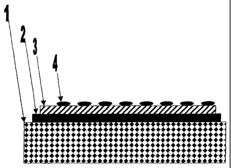
Fig. 1-6 present examples of security features according to the invention.
In these figures. 1 designates the base substrate, 2 the electromagnetic wave-
reflecting first layer,
3 the transparent layer, 4 the layer constructed of metallic clusters, 5 an
optically transparent
substrate, 6 an adhesive or lamination layer.
Fig. 1 shows a schematic cross-section through a first continuously visible
marking on a base
substrate.
CA 02494961 2010-08-20
16a
Fig. 2 shows a schematic cross-section through a non-continuously visible
first marking on a base
substrate, as well as a second base substrate suitable for verification or
rendering the marking
visible.
Fig. 3 shows a schematic cross-section through a continuously visible first
laminatable or adhesive
marking.
Fig. 4 shows a schematic cross-section through another continuously visible
second laminatable or
adhesive marking.
Fig. 5 shows a schematic cross-section through a non-continuously visible
first laminatable or
adhesive marking, as well as a second base substrate suitable for verification
or rendering the
marking visible.
CA 02494961 2005-02-07
17
Fig, 6 shows a continuously coated forgery-proof marked base substrate in
large-scale format,
which is partially rolled up onto rollers.
In the markings shown in Fig. 1 to 5. an electromagnetic wave-reflecting first
laver is designated
with (2). This can be a thin layer made of. e.g.. aluminum. The first laver
(2) can, however, also
be a layer formed of metallic clusters, which is applied to a substrate (1).
The substrate (1) can be
the base substrate which is to be marked. The inert spacer laver is designated
with (3). The
metallic clusters (4) are expediently produced, e.g.. from copper.
In Fig. 3 to 5, the adhesive or lamination layer provided for further
processing of the forgery-
proof marked base substrate is labeled with (6). The change in the reflected
light versus the
incident light which creates the characteristic color spectrum is visualized
in these two figures
using a grayscale gradient in an arrow.
In the markings shown in Fig. I and 3, a third layer (4) produced from metal
clusters is applied
to the second layer (3), with the second layer (3) being applied to a
reflecting layer (2). In
addition, in Fig. I and 3, the reflecting layer is applied to a base substrate
(1).
In Fig. 4, first the third laver (4) formed of metallic clusters is applied to
a base substrate (1), then
the second layer (3), then the reflective layer (2) and finally the adhesive
or lamination layer (6).
CA 02494961 2005-02-07
18
In the markings shown in Fig. 2 and 5, only the optically transparent second
layer (3) is applied
to the electromagnetically reflecting first layer (2), which is applied to a
base substrate (1). The
marking is initially not visible. The markings only become visible when
brought into contact
with a substrate (5). which has a third layer (4) formed from metallic
clusters applied to its
surface. A color effect then appears, which is visible through the substrate
(5). The base substrate
(5) is expediently produced from a transparent material, e.g., from plastic.
such as polyethylene
terephtalate polycarbonate. polyurethane, polyethylene. polypropylene,
polyacrylate, polyvinyl
chloride, polyepoxide.
The marking functions as follows:
When light from a light source. such as a light bulb, laser. fluorescent lamp,
halogen lamp, in
special cases a xenon lamp, shines onto one of the markings shown in Fig. 1, 3
and 4. this light is
reflected by the first layer (1). Due to an interaction between the reflected
light and the third
layer (4), formed of metallic clusters, a portion of the incident light is
absorbed. The reflected
light exhibits a characteristic spectrum which depends on a number of
parameters, such as, e.g.,
the optical constants of the layer construction. The marking appears colored.
The coloration
serves to provide forgery-proof verification
CA 02494961 2010-08-20
19
of the authenticity of the marking. The resulting color effect depends on the
viewing angle and
can be identified with the naked eye as well as with a reading device
operating in reflection
mode, preferably a spectral photometer. A photometer such as this can, for
example, record the
coloration of the surfaces from two different angles. This is done either with
one detector, using
two light sources which are powered on appropriately and appropriately tilted
relative to the
detector, or by using two photometers to take measurements of the sample at
the two angles at
which it is illuminated.
The parameters which must be adhered to for the interactions to be generated
are disclosed in US
5,61 1,998, WO 98/48275 and WO 99/47702 and WO 02/18155.
The coated base materials produced according to the invention can be used as
security features in
data media, documents of value, labels, tags, seals, in packaging, textiles
and the like.
CA 02494961 2005-02-07
Examples:
Example l:
Production of the cluster layer using wet chemical methods:
a) Synthesis of 14 nm gold clusters
100 ml aqua dest is heated to boiling in a 250 ml flask. While stirring
vigorously, first 4 ml I %
trisodium citrate in aqua dest and then I nil 1 % tetrachloro gold acid in
aqua dest are added.
Within a period of 5 min, the color of the reaction solution changes from
nearly colorless to dark
violet to cherry red. The supply of heat is then ended and the solution
stirred further for
approximately 10 min. Transmission electron microscope analysis of the
resulting so] shows
spherical particles having an average diameter of 14 nm. The clusters have a
narrow size
distribution (cv < 20 %). The maximum wavelength of optical absorption is 518
nm.
b) Derivatization of the gold clusters:
While stirring vigorously, I ml of a I % solution of BSA (Bovine Serum
Albumin) in aqua dest
is added to 100 ml of gold sol prepared according to the above synthesis. The
solution changes
color slightly from cherry red to a dark red. The optical absorption maximum
remains
unchanged. Absorption increases for wavelengths in the range of 550 nm and
above. Defined
separations between the particles can be seen in the transmission electron
microscope.
c) Binding the gold clusters to a nitrocellulose surface:
CA 02494961 2005-02-07
21
The sot (nearly pH neutral, almost no salt) is rebuffered by adding 5 ml I M
sodium carbonate
solution (pH 9.6). Only sufficiently protected clusters remain in solution and
do not precipitate
out. The sol can be concentrated by centrifuging or hinds directly after
application to the
nitrocellulose-coated surface. When the thickness of the
nitrocellulose layer is chosen appropriately, strong surface colorations form
after the excess
water has dried.
Example 2:
Production of the cluster layer using printing methods
After concentrating the sol by a factor of 10, small amounts (e.g., 5 %) of a
neutral polymer (e.g.,
PVA) are admixed to the sol. This makes printing with the usual intaglio
printing cylinders
possible. The colloids dry randomly oriented with the polymer in a very thin
layer. Characteristic
colors are observed as in Example I c.
Example 3:
Production of the cluster layer using a vacuum method
CA 02494961 2005-02-07
22
Under high vacuum conditions (base pressure p < l x 10 mbar). a 4 run-thick Cu
layer is
sputtered onto a strip-shaped base substrate which has already been provided
with a reelecting
layer and a nitrocellulose layer acting as a transparent spacer layer.
The sputtering is performed using a magnetron plasma source with an output of
20 W/cm2 at 25
C and Ar with a partial pressure of 5 x 10 mbar as the process gas. The strip
speed is 0.5 m/s.
Under these conditions. the Cu layer shows distinct island growth. The islands
with an average
diameter of several nm correspond to the clusters in the wet chemical method.
Other characteristic color spectra are clearly observed.