Note: Descriptions are shown in the official language in which they were submitted.
"~ CA 02495358 2005-O1-28
PATENT
81088-243301
TITLE OF THE INVENTION
POWER FACTOR CORRECTION CIRCUIT'S
BACKGROUND OF THE INVENTION
1. Technical Field
This invention relates to power adapters, and more specifically, to a system
and method
to correct power factor, i.e., the ratio of real power to apparent power.
2. Description of the Related Arts
The explosive growth in consumer electronic:. is causing the electricity
supply industry
considerable concern. The appliances or consumer e:.ectronics devices employ
power supplies
that draw current from the AC power line during the peak of the sine wave.
Most of the
appliances or consumer electronics device utilize a rectifier-bridge/smoothing
capacitor circuit.
Power factor is the ratio of real power to apparent power. In the United
States, power is
provided at approximately 120 Volts AC with a frequency of approximately 60
Hertz. In Europe
and other areas, power is provided at approximately :'40 Volts AC with a
frequency of
approximately 50 Hertz. In order to provide a maximum amount of usable energy
or power, it is
desirable for a load to draw current as if the load is entirely resistive. If
the load appears
resistive, then the current drawn from the source ma3~ have a substantially
sinusoidal shape, as
the AC voltage has, and the current drawn from the source may be in phase with
the AC input
voltage.
Power supplies that utilize rectifier-bridge / smoothing capacitor circuits
draw non-
sinusoidal currents as the AC line's instantaneous voltage exceeds the storage
capacitor's
voltage. The electricity generator, with no power factor correction, must
supply energy at the
20490516v1
CA 02495358 2005-O1-28 ~--
PATENT
81088-243301
top/peak of the sine wave rather than throughout the cycle, which can cause
the sine wave to
collapse around its peak.
The electricity generator sees the phase lag between the current and voltage,
together
with the harmonics from peaky loads, as combining to provide require rms
currents, which in
turn reduces the real power that the network can supply. Varying loads at the
consumer end of
the line produces fluctuations throughout the local line and these
fluctuations cause undersirable
consequences, such as causing lighting sources to flicker.
Fig. 1 illustrates the current and voltage wavePorms for an electronic device
that power
factor correction (PFC) is designed to correct according to the prior art. As
illustrated, the
voltage waveform is sinusoidal in shape and the currE;nt waveform can be
characterized as a
waveform with a steady current value with large spikes in the amplitude of the
current waveform
along with a high content of harmonics. The large spikes in the current
waveform are caused
because of the switching power supplies' use of the rectifier bridge /
smoothing capacitor
circuits. From an eff-lciency viewpoint, a typical uncorrected switched-mode
power supply has a
power factor of 0.6, which effectively reduces the current available from the
AC socket from
about 13 to about 7.8 Amps.
A solution for power factor correction is to c~~ndition the equipment's input
Load power
so that it appears purely resistive using active PFC tcxhniques. Common PFC
designs employ a
boost preconverter ahead of the conventional voltagc; regulation stage, which
effectively
cascades to switched-mode power supplies. The boast preconverter raises the
full-wave
rectified, unfiltered AC line to a DC input rail at a level slightly above the
rectified AC line,
which is typically around 375 to 400 volts DC. By drawing current throughout
the AC line
20490516v1 2
CA 02495358 2005-O1-28
PATENT
81088-243301
cycle, the boost preconverter forces the load to draw c:urrent in phase with
AC line voltage,
quashing harmonic emissions.
Fig. 2 illustrates a power factor correction circuit with a boost preconverter
according to
the prior art. The full-wave bridge rectifier 200 receives the AC input
voltage and produces a
full-wave rectified voltage. The boost preconverter 205 receives the full-wave
rectified voltage
and forces the load to draw current in phase with the voltage. The shape of
the current waveform
is determined by a switching device 21 S, which is coupled to the output and a
control circuit 220.
The control circuit 220 provides an input to the switching device 215 and
receives as input
signals a signal from the output and a signal from the rectifier/boost node
225. This circuit may
solve the power factor problem by shaping the current waveform to mimic the
voltage waveform
and to cause the current waveform to be in phase with the voltage waveform.
However, the
circuit utilizes at least five diodes, four of which are located in the bridge
rectifier, and diodes are
lossy components, which decreases the power efficiency of the circuit.
Accordingly, it would be beneficial to have fc;wer lossy components in a power
factor
correction circuit, where the power factor correction circuit accepts a wide
range of input
voltages and automatically adjusts the current wavef~rm provided to be
substantially sinusoidal
in shape and in phase with the AC input voltage waveform.
It would also be beneficial to utilize the circuitry that is rectifying the AC
input voltage to
assist in providing power factor correction.
BRIEF DESCRIPTION OF THE DRAWINGS
Fig. 1 illustrates a current and voltage waveforms for an electronic device
that power
factor conversion is designed to correct according to the prior art;
20490516v1
CA 02495358 2005-O1-28
PATENT
81088-243301
Fig. 2 illustrates a power factor correction circuit with a boost preconverter
according to
the prior art;
Fig. 3 illustrates a bi-directional boost circuit for power factor correction
in a power
adapter according to an embodiment of the present invention;
Fig. 3(a) illustrates programming resistors wi~:hin a cable according to an
embodiment of
the present invention;
Fig. 3(b) illustrates programming resistors with a connector according to an
embodiment
of the present invention;
Fig. 4 illustrates a bi-directional boost circuit for power factor correction
according to an
embodiment of the present invention;
Fig. 5(a) illustrates a haversign signal according to an embodiment of the
present
invention.
Fig. 5(b) illustrates a ramp signal and a DC e:xor signal according to an
embodiment of
the present invention;
Fig. 5(c) illustrates a pulsed signal according to an embodiment of the
present invention;
Fig. 6(a) illustrates the inductor current output, as seen by the input power
source,
including the high frequency pulses in the substantially sinusoidal envelope,
according to an
embodiment of the present invention;
Fig. 6(b) illustrates a clipped inductor current. waveform as seen by the
power source
according to an embodiment of the present invention;
Fig. 7 illustrates a schematic of a power factor correction circuit according
to an
embodiment of the present invention;
20490516v1
CA 02495358 2005-O1-28
PATENT
81088-243301
Fig. 8(a) illustrates a waveform created by a first waveform generator
according to an
embodiment of the present invention;
Fig. 8(b) illustrates a waveform created by a second waveform generator
according to an
embodiment of the present invention;
Fig. 8(c) illustrates a combination waveform generated by a first waveform
generator and
a second waveform generator according to an embodiment of the present
invention;
Fig. 9(a) illustrates a second embodiment of the power factor correction
circuit according
to an embodiment of the present invention;
Fig. 9(b) illustrates current flow during the positive cycle of the AC input
according to an
embodiment of the present invention; and
Fig. 9(c) illustrates a current flow during the negative cycle of the AC input
according to
an embodiment of the present invention.
DETAILED DESCRIPTION
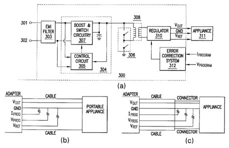
Fig. 3 illustrates a bi-directional boost circuit for power factor correction
according to an
embodiment of the present invention. The boost power factor conversion circuit
may be utilized
in an AC to DC power adapter or power converter. f: is desirable for the power
adapter to appear
to the power supply line as a resistive load. In other words, the current
waveform should be in
phase and have approximately the same shape as the voltage waveform. This
minimizes the
demand on the utility provider because large, potentis~lly instantaneous
spikes of current demand
may be avoided.
The power adapter 300 may include a pair of AC input terminals 301 and 302, an
electronic magnetic interference (EMI) filter 303, a bi-directional boost
circuit 304, a switching
device 306, a transformer 308, a regulator 310, and a~i error correction
system 312. The power
20490516v1
CA 02495358 2005-O1-28 ~-.
PATENT
81088-243301
adapter 300 may produce a power output having a regulated output voltage and a
controlled
output current.
The EMI filter 303 removes high-frequency noise from the power adapter. The bi-
directional boost circuit 304 produces an intermediatc; DC voltage. In
addition, the bi-directional
boost circuit 304 provides power factor correction for the inductor current,
as seen by the power
source, and reduces any instantaneous current deman3 spikes. The power adapter
300 may
achieve power factor correction by utilizing the bi-directional boost circuit
304 to generate a
current waveform, as seen from the power source, that is substantially
sinusoidal in shape and in
phase with the AC input voltage. The bi-directional boost circuit 304 includes
a control circuit
305 and a rectifying correction circuit or boost / swit~;h circuitry 307. The
rectifying correction
circuit 307 receives the AC input voltage and produces an intermediate DC
output voltage by
converting and rectifying the AC input voltage. The control circuit 305
receives the intermediate
DC output voltage and the AC input voltage. Based ~~n the intermediate DC
output voltage and
the AC input voltage, the control circuit 305 transmits a signal to cause the
rectifying correction
circuit 307 to generate a current waveform, as seen b;y the power source, that
is substantially
sinusoidal in shape and in phase with the AC input voltage. The bi-direction
boost circuit 304
only utilizes two diodes so the number of lossy components is reduced and the
power adapter
efficiency is improved. Additionally, the bi-directional boost circuit 304
utilizes the same
circuitry to boost and rectify the AC input voltage an~3 also to generate a
current waveform that is
substantially sinusoidal in shape and is in phase with the AC input voltage.
The current
waveform may be an inductor current waveform or the current waveform as
measured at the
inductor in the boost / switch circuitry 307.
20490516v1
CA 02495358 2005-O1-28
PATENT
81088-243301
The intermediate DC voltage is input to the sv~ritching device 306, which
outputs a
switched output. The switched output is input to a transformer 308, which
outputs a second
intermediate voltage. The second intermediate voltage is output to a regulator
310, which
generates a power output with a regulated voltage and a controlled current.
The power output is
provided to a portable appliance 311. Because the power requirements of the
portable appliances
vary, e.g, CD players, need one input voltage and cell phones a second input
voltage, the power
output of the power adapter may be regulated, a~s desc;ribed below. Generally,
a programming
signal, i.e., a voltage programming signal or a current: programming signal,
may be provided to
an error correction system 312 and the error correction system 312 can
transmit a signal to the
regulator 310 to regulate the output voltage or to conool the output current.
Specifically, the regulator 310 may receive th~~ second intermediate voltage.
In an
embodiment of the invention, the regulator 310 may he a buck regulator, a
boost regulator, or a
buck-boost regulator, or any other regulator commonly utilized in the power
adapter art. The
regulator 310 generates a power output including a regulated voltage and a
controlled current.
The power output is provided to the portable appliance. Because different
portable appliances
have different operating voltage requirements and cu:rent needs, the power
adapter 300 may
need to be configured to output the necessary regulated voltage and/or
controlled current.
The regulated voltage and the controlled current output from the regulator 310
is also
input to an error correction system 312. The error correction system 312 may
also receive a
programming signal. The magnitude of the programming signal may be dependent
upon a value
of a resistor located in a cable coupled to the power supply. In an embodiment
of the invention,
the magnitude of the programming signal rnay be deF~endent upon a value of a
resistor located in
a connector coupled to the cable and the power suppl y. Fig. 3 (a) illustrates
a cable with
20490516v1 7
CA 02495358 2005-O1-28
PATENT
81088-243301
programming resistors coupled to the power adapter and Fig. 3(b) illustrates a
connector with
progra><nming resistors coupled to a cable and a power- adapter according to
an embodiment of
the invention. In an embodiment of the invention, one or more resistors may be
installed in one
of the cable and the connector. The installation of the; one or more resistors
in the one of the
cable and the connector and the coupling of the cable or the cable and the
connector, may change
the magnitude of the programming signal to be transmitted to the error
correction system 312.
Illustratively, the one or more resistors may b~~ coupled between a line in
the cable or
connector coupled to voltage program input and a line in the cable or
connector coupled to
ground. Illustratively, the one or more resistors may be coupled between a
line in the cable or
connector coupled to current program input and a line in the cable or
connector coupled to
ground. Illustratively, a first resistor may be coupled between a reference
output and ground and
a second resistor may be coupled between voltage pr~~gram input and ground.
This may produce
a different magnitude of the programming signal because the first resistor may
be coupled in
parallel with a pullup resistor in the power adapter, which may modify the
resistance value.
Description of the resistors within the cable and the connector are found in
the following patents,
the disclosures of which are incorporated herein by n~ference: U.S. Patent No.
5,838,554,
entitled "Improved Small Form Factor Power Supply;" U.S. Patent No. 5,949,213,
entitled
"Method and System for Recharging Batteries;" U.S. Patent No. 6,172,884,
entitled
"Programmable Power Supply;" and U.S. Patent No. 6,266,261, entitled "DC Power
Adapter
System."
Alternatively, a programming signal may be transmitted from an active device
in the
cable or from an active device in the connector. The active device may be a
controller or an
operational amplifier. The active device may transmit the programming signal
to the error
20490516x1
CA 02495358 2005-.O1-28
PATENT
81088-243301
correction system 312. The active device may receive: a voltage reference
signal from the power
adapter 300. Further discussion of such active devices are provided in the
following patent
applications, the disclosures of which are incorporated by reference: U.S.
patent application
serial No. 10/313,662, filed May 30, 2003, entitled "E,ctive Tip", and U.S.
patent application
serial No. 10/313,793, filed December 6, 2002, entitled "Programmable Tip."
Specifically, Fig. 4 illustrates an example of a bi-directional boost circuit
for power factor
correction according to an embodiment of the present invention. In Fig. 4, the
bi-directional
boost circuit 307 of Fig. 3 is presented in more detail. The bi-directional
boost circuit may
include a first terminal 501, a second terminal 502, a first inductor 503, a
second inductor 504, a
first diode 506, a second diode 508, an output tertnin~~l 510, a first switch
512, a second switch
514, and a capacitor 520. The control circuit 305 of l~ig. 3 (control circuit
516 in Fig. 4) may
include an error amplifier 531, a pulse width modulator 530, a waveform
generator 532, an
integrator 534, and a pair of switch control circuits 5..6 and 538.
The first terminal 501 may be coupled to the rust inductor 503, which may be
coupled to
the first diode 506 and a terminal of the first switch 512. The second
terminal 502 may be
coupled to the second inductor 504, which may be coupled to the second diode
508 and a
terminal of the second switch 514. The first diode 506 and the second diode
508 may be coupled
to the output terminal 510, along with a terminal of the capacitor 520, the
other terminal of the
capacitor 520 being coupled to ground. The control circuit 516 may be coupled
to the output
terminal 510, the first terminal 501, and the second terminal 502. The control
circuit 516 may be
coupled to the first switch 512 and the second switch 514. In an embodiment of
the invention,
the control circuit 516 may be coupled to a control tel~rninal of the first
switch 512 and a control
20490~16v1
CA 02495358 2005-O1-28 ~-...
PATENT
81088-243301
terminal of the second switch 514, e.g., gate terminals when the first switch
512 and the second
switch 514 are Field Effect Transistors.
The first terminal 501 and the second termina.~. 502 provides the AC input
voltage from an
input power source. The first inductor 503, the second inductor 504, first
diode 506, the second
diode 508, the first switch 512, and the second switch 514 receive the AC
input voltage, converts
the AC input voltage, rectifies the AC input voltage, ~~nd produces an
intermediate DC output
voltage, as discussed further below.
The first switch 512 may be a field effect transistor (FET) that has a first
terminal
coupled to the junction between the first inductor 50.. and the first diode
506. The second switch
514 may be a FET and have a first terminal coupled ~:o the junction between
the second inductor
504 and the second diode 508. A second terminal of the first switch 512 and a
second terminal
of the second switch 514 may be coupled to ground:
During the positive cycle of the AC input, i.e., if a voltage at terminal 501
is greater than
a voltage at a terminal 502, and the first switch 512 i ~ on, energy is stored
in the first inductor
503. If the first switch 512 is off, the energy stored in the first inductor
is transferred through the
first diode 506 to the capacitor 520. This causes the capacitor 520 to charge
to a steady state DC
voltage Vpos during the positive cycle of the AC input. The combination of the
first diode 506
and the first switch 512 are utilized to rectify the AC input in the positive
cycle. In an
embodiment of the invention, the capacitor 520 may also smooth the ripple of
the rectified DC
output voltage.
During the negative cycle of the AC input, e.g., if a voltage at terminal 502
is greater than
a voltage at terminal 501, and the second switch 514 is on, energy is stored
in the second
inductor 504. If the second switch 514 is not on, the energy stored in the
second inductor 504 is
20490516v1 1 0
CA 02495358 2005-O1-28
PATENT
81088-243301
transferred through the second diode 508 to charge up the capacitor 520 to a
steady state voltage
Vpos2. In an embodiment of the invention, the switc'.Zes 512 and 514 may have
an operational
frequency of 80 to 120 Kilohertz. Although the magnitude of the AC input is
negative during the
negative cycle of the AC input, the current is flowing to the capacitor 520 in
the same direction
as the current flowing during the positive cycle of the AC input, and thus the
voltage across the
capacitor 520 is positive. The combination of the second diode 508 and the
second switch 514
are utilized to rectify the AC waveform. In an embodiment of the invention,
the capacitor 520
may also smooth the ripple of the rectified DC outpu:. The intermediate DC
output voltage is the
addition of steady-state voltages Vpos and Vpos2, and has the shape of a
rectified waveform, as
smoothed by the filtering action of the capacitor 520.
The AC input voltage may also be provided to the power factor control circuit
516. In
addition, the power factor control circuit 516 may re<;eive the intermediate
DC output voltage
from the output terminal 510. The control circuit 51 ~i may utilize the AC
input and the DC
output to create driving signals that are respectively input to the control,
e.g., gate, terminals of
the first switching device 512 and the second switching device 514. The
control circuit 516 may
control the current in the inductors 503 and 504 and may cause an inductor
current to have a
substantially sinusoidal shape. The substantially sinusoidal shape of the
inductor current
corresponds to a haversign signal generated within tree control circuit 516
except that the
inductor current sinusoidal waveform crosses a line, e.g., a reference
potential while the
haversign signal waveform does not cross a line on a graph and stays positive,
the line, for
example, representing a reference potential.
Specifically, the AC input voltage may be inlrut to a waveform generator 532.
The
waveform generator 532 may generate a haversign waveform, as illustrated in
Fig. 5(a). The
20490516v1 1 1
CA 02495358 2005-O1-28
PATENT
81088-243301
intermediate DC output voltage is input to an error amplifier 531. The
intermediate DC output
voltage is compared to a reference voltage and a DC f;rror signal is output
from the error
amplifier 531. A pulse width modulator 530 receives the DC error signal from
the error
amplifier 531 and compares the DC error signal to a ramp signal. In an
embodiment of the
present invention, the ramp signal may be oscillating in a frequency range of
80 - 120 Kilohertz.
The DC error signal is illustrated as a dotted line in Fig. 5(b) and the ramp
signal is illustrated as
a solid line in Fig. 5(b). The pulse width modulator _'~30 outputs a pulsed
signal. Illustratively,
the pulsed signal for the comparison of the DC error ;signal and the ramp
signal is illustrated in
Fig. 5 (c).
The haversign waveform and the pulsed sign~~l are multiplied together to
create a
multiplied haversign waveform, which is input to an integrator 534. The
amplitude of the
multiplied haversign waveform is controlled by the pulsed signal. The
integrator 534 strips off
the high frequency characteristics of the multiplied haversign waveform and
produces a
haversign signal.
In an embodiment of the invention, a haversil;n signal may be input to a first
switch
control circuit 536 and a second switch control circuit 538. During the
positive cycle of the AC
input, the first switch control circuit 536 monitors thc; actual current in
the first inductor 503.
The first switch control circuit compares a magnitudc; of the inductor current
in the first inductor
503 to a threshold value, e.g., a magnitude of the haversign signal at
specific point in time.
When the inductor current is greater than the magnitude of the haversign
signal input to the first
switch control circuit 536, the first switch control circuit transmits a first
drive signal to turn off
the first switch 512. Because the haversign signal is sinusoidal in shape, the
inductor current
output during the positive cycle of the AC input from the first switch 512 may
also have a
20490516v1 1 2
CA 02495358 2005-O1-28
r
PATENT
81088-243301
sinusoidal shape. The frequency of a signal output from the first switch
control circuit 536 is a
high frequency, e.g., in the range of 80 Kilohertz to 1:Z0 Kilohertz. Because
the first switch 512
is fuming on and off at the high frequency, the inductor current output is
actually a series of high
frequency pulses operating which are formed in a substantially sinusoidal
envelope, where the
sinusoidal envelope is oscillating between 45 - 65 Hertz. Fig. 6(a)
illustrates the inductor current
output, as seen by the input power source, including the high frequency pulses
in the
substantially sinusoidal envelope. This may be referred to as an inductor
current including a
substantially sinusoidal shape. Due to the high frequency at which the first
switch 512 operates,
Fig. 6(a) is not drawn to scale.
During the positive portion of the input AC waveform, the second switch 514 is
always
on because a threshold value is never reached, i.e., the inductor current
measured in the second
inductor 504 by the second switch control circuit 538 never reaches the value
of the haversign
signal input to the second switch control circuit 538. Therefore, the second
switch 514 is always
turned on during the positive cycle of the AC waveform.
The haversign signal is also input to the second switch control circuit 538
and the second
switch control circuit 538 outputs a second drive signal to drive the second
switching device 514
during the negative cycle of the AC input. Again, because the haversign
waveform is sinusoidal
in shape, the inductor current, as seen from the powex source, may also be
sinusoidal in shape,
i.e., may be a number of high frequency pulses that ride in a substantially
sinusoidal envelope.
During the negative cycle of the AC input, the magnitude of this substantially
sinusoidal
waveform may be negative, unlike the haversign signal which has a positive
magnitude.
The power source may see the inductor current waveforms during the positive
cycle and
the negative cycle of the AC input as a substantially sinusoidal waveform that
is in phase with
20490516vt 1 3
CA 02495358 2005-O1-28
PATENT
81088-243301
the AC input voltage. Power factor correction is achi~.ved because the
substantially sinusoidal
waveform is resistive in nature and the instantaneous peak demands for current
has been reduced
or eliminated.
In an embodiment of the invention, the first switch control circuit 536 and
the second
switch control circuit 538 may limit the amplitude of the inductor current.
This may be
beneficial for use in the United States, where power f actor correction is not
required, and thus the
inductor current may not need to be sinusoidal in shape. In order to output
the necessary power
within the United States, approximately double the arnount of current may need
to be utilized in
order to produce the same power with half the currern: in Europe. This large
amount of current
may require larger size inductors to handle the amount of current in the
device which may result
in less efficiency of the power supply. This loss of efficiency may be
neutralized by clipping the
substantially sinusoidal waveform of the inductor current as seen from the
power source, i.e:,
limiting the peak current of the sinusoidal waveform, and producing more of a
trapezoidal- or
square-shaped inductor current waveform.
In this embodiment of the invention, the first ;witch control circuit 536 may
limit the
amplitude of the inductor current on the positive half of the AC input if the
magnitude of the
inductor current exceeds a clipping threshold value. :gin other words, the
first switch control
circuit 536 clips the peak of the inductor current wav~:form, making the
waveform have more of
a square-wave or a trapezoidal shape as seen by the power source, rather than
a sinusoidal shape.
In this embodiment, the peak current in the inductors is lower. During the
negative cycle of the
waveform, the second switch control circuit 538 may also limit the amplitude
of the inductor
current if the magnitude exceeds the clipping thresho::d value. Fig. 6(b)
illustrates an ideal
version of a clipped inductor current waveform as seen by the power source
according to an
20490516v1 1 4
CA 02495358 2005-O1-28
PATENT
81088-243301
embodiment of the present invention. Again, the actual inductor current would
be a series of
high frequency pulses which are either square or trapE;zoidal in shape. A
clipping threshold
value may be set by installing a component across pins of the first switch
control circuit 536 or
the second switch control circuit 538. Fig. 6(b) illusta-ates the high
frequency pulses that create
the clipped inductor current waveform. Again, Fig. 6(b) is not drawn to scale
due the high
frequency of the switches being activated.
Fig. 7 illustrates a schematic of the power facv:or correction circuit
according to an
embodiment of the present invention. A first terminal 601 of the AC line is
coupled to a first
terminal of a first inductor 604 and a waveform gene;-ator 670 (through AC-A).
A second
terminal 602 of the AC line is coupled to a first terminal of a second
inductor 605 and the
waveform generator 670 (through AC-B). A second terminal of the first inductor
604 is coupled
to a first diode 610 anode and is coupled an output terminal of a first
switching device 614. A
second terminal of the second inductor 605 is couple3 to a second diode 612
anode and an output
terminal of a second switching device 616.
The control terminal of the first switching de~rice 614 is coupled to the
first current mode
controller 617. The control terminal of the second switching device 616 is
coupled to the second
current mode controller 618. The first diode 610 cathode and the second diode
612 cathode are
coupled to the output terminal 640 of the power facts>r correction circuit
600. The output
terminal 640 is coupled to a first error amplifier 620 and also may be coupled
to a second
amplifier 652.
The error amplifier 620 compares a reference voltage with the high voltage
intermediate
DC output present at the output terminal 640. The error amplifier 620 outputs
a voltage error
signal. For example, in the embodiment of the invention illustrated in Fig. 7,
the voltage input to
20490516v1 1 5
CA 02495358 2005-O1-28 ~.
PATENT
81088-243301
the inverting input of the error amplifier 620 may be approximately 5.0 volts,
which is
determined after the high voltage DC output is input t~~ a voltage divider
network created by
resistors R26 and R27. In the embodiment of the invention illustrated in Fig.
7, the voltage input
to the inverting input of the error amplifier 620 may be compared to a
reference voltage of 5.1
volts.
The voltage error signal output from the error amplifier 620 may be input into
a pulse
width modulator 630. The pulse width modulator 630 may compare a periodic ramp
signal with
the DC signal output from the error amplifier 620. The pulse wide modulator
630 may generate
a pulsed signal. In an embodiment of the invention, the ramp signal may be
generated by the
1 U current mode controllers 617 and 618. For example, the values of the
resistor R17 and capacitor
C6 attached to pin 4 of the current mode controller 6'..8 may determine the
frequency of the ramp
signal, as illustrated by the box marked Ramp in Fig '7.
The pulsed signal may be multiplied by a haversign signal generated by a
waveform
generator 670. The waveform generator 670 may include a first waveform
generator 671 and a
second waveform generator 672. Fig. 8(a) illustrates a waveform created by a
first waveform
generator according to an embodiment of the invention. A first waveform
generator 671 receives
the AC input from terminals 601 and 602 and acts as a differential amplifier
to create a
sinusoidal shaped waveform for a positive cycle of tile AC input and no
waveform for the
negative cycle of the AC input, as illustrated in Fig. !~(a). A second
waveform generator 672
receives the AC input from terminals 601 and 602, except the second waveform
generator
subsystem has the signal from terminal 601 input to t:he non-inverting input
of the operational
amplifier U4B and the signal from terminal 602 input into the inverting input
of the operation
amplifier U4B, which is opposite to the inputs to the first waveform
generator. Fig. 8(b)
20490516v1 1 6
CA 02495358 2005-O1-28 ~..
PATENT
81088-243301
illustrates a waveform created by a second waveform generator according to an
embodiment of
the present invention. The second waveform generator 672 creates a sinusoidal
waveform
opposite in phase to the waveform generated by the first waveform generator
subsystem 671, as
illustrated in Fig. 8(b), i.e., a sinusoidal waveform is generated during the
negative cycle of the
AC input and no waveform is generated during the positive cycle of the AC
input.
The output of the first waveform generator 671 and the second waveform
generator 672
are summed at node 675. The resulting waveform is a haversign waveform, as
illustrated in Fig.
8(c).
The multiplication of the haversign and the pulsed signal may produce a
multiplied
haversign output at node 676. In other words, the pulsed signal may control
the magnitude of the
haversign.
The integrator 650 strips the multiplied haversign output of high frequency
characteristics
created by the pulse wide modulator's 630 operating frequency and creates an
integrated
haversign waveform. The high frequency characteri:;tics are generated by the
pulse width
modulator 630 pulsing at the ramp signal frequency. In one embodiment of the
invention, the
ramp signal frequency may be 100 Kilohertz. As illustrated in Fig. 7, the
integrator 650 may be
formed by a resistor R15 and a capacitor C19.
Comparator USA 652 may respond to instant~3neous large changes in the
magnitude of
the intermediate DC output voltage. Comparator USA 652 may generate a clamp
signal to
prevent the control circuit from responding to large instantaneous changes in
intermediate DC
output voltage magnitude. If the large instantaneous change in the magnitude
of the intermediate .
DC output voltage is detected by USA 652, U5A 652 may output a signal to clamp
the integrated
haversign waveform.
20490516v 1 17
CA 02495358 2005-O1-28
PATENT
81088-243301
U4C 654 is a buffer for the integrated haversi~;n waveform and outputs a
haversign
signal. The integrated haversign waveform is input to the non-inverting input
of the amplifier
and the feedback signal from U4C 654 is input to the inverting input of U4C
654. These
connections enable the operational amplifier U4C 65~~ to have a unity gain at
the output and to
operate as a buffer.
A control circuit 680 controls current in the inductors L2 (L2-A and L2-B) 604
and L3
(L3-A and L3-B) 605. The current in the inductors 604 and 605 is controlled by
having the
current track the voltage output, i.e., the haversign sil~al, from U4C 654.
The current mode
controllers 617 and 618 control the current flow through the inductors 604 and
605 by turning off
and on switches 614 and 616, respectively. The input to the current mode
controllers 617 and
618 is a voltage from U4C with a waveshape of a haversign, i.e., a haversign
signal. For
example, the current mode controllers 617 and 618 are voltage-to-current
converters so the
inductor current tracks the waveform shape of the ha~ersign signal input to
the current mode
controllers 617 and 618. When the AC input reverses, i.e., goes to the
negative cycle, the
inductor current is traveling in the opposite direction. i.e., has a negative
value, and instead of
precisely tracking the haversign signal, the inductor current waveform
maintains the shape of the
haversign signal, but the inductor current is negative with respect to a
reference potential and the
inductor current crosses the reference potential when the AC input reverses.
Therefore, the
resulting AC waveform is a substantially sinusoidal current that crosses a
reference potential
when it switches from a positive cycle to a negative cycle.
The current mode controllers 617 and 618 receive the haversign signal from the
buffer
U4C 654. In the embodiment of the invention illustrated in Fig. 6, the
haversign signal is input
to pins 1 and 2 of current mode controllers 617 and 618. During the positive
cycle of AC input,
20490516v1 1 g
CA 02495358 2005-O1-28
PATENT
81088-243301
e.g., when the voltage at terminal 601 is greater than the voltage at terminal
602, the current
mode controller 617 monitors the inductor current through inductors L2 604. In
an embodiment
of the invention, the current mode controller 617 monitors the inductor
current via pin 3 by
measuring the current across resistor R22. The current mode controller 617
compares the
monitored inductor current to a threshold value. Illustratively, the threshold
value is the input
from buffer U4C 654, which is a value of the haversi3~ signal at an instant in
time. If the
monitored inductor current is larger than the threshold value, then the
current mode controller
617 may turn off the switching device 614. In other ~HOrds, the current mode
controller 617 is
allowing the inductor current to track up the value of the haversign signal at
that moment in time,
but does not allow the inductor current to go higher than the value of the
haversign signal. Thus,
the current in the inductor 604 tracks the haversign waveform.
The current mode controller 618 activates switch 616 continuously during the
positive
cycle of the AC input. The current mode controller E~18 monitors the current
in the inductors 605
and compares it to the threshold value. The inductor current being monitored
has a negative
value, however, because the current is flowing from ~:ommon ground through the
switch 616 and
back to the inductor 605. Because the threshold value is positive, the current
value never reaches
the threshold value and switch 616 is continuously activated during the
positive cycle of the AC
input. For example, during the positive cycle of the .~C input, the current
path is from inductors
604 through switch 614 through resistor R22 to common ground. Then, the
current path returns
from common ground through resistor R29 through switch 616 and to inductors
605. The
current mode controller 618 is monitoring the inductor current, which is
flowing in a negative
direction through the resistor which is utilized for monitoring, e.g., R19.
Because the value of
20490516v1 1 9
CA 02495358 2005-O1-28
PATENT
81088-243301
the inductor current is negative, the value of the inductor current never
reaches the threshold
value, and switch 616 is always turned on during the positive cycle of the AC
input.
Conversely, when the AC input is in a negative cycle, the value of the AC
input at
terminal 602 is greater than the value of the AC input at terminal 601,
current mode controller
618 turns on and off switch 6I6 and current mode controller 617 turns switch
614 on
continuously. Illustratively, during the negative cyclf: of the AC input, the
current mode
controller 618 is monitoring the inductor current in inductors 605 when switch
616 is on via
resistor R19. The current mode controller 618 comperes the inductor current to
the value of the
haversign signal input from buffer U4C 654. If the inductor current is larger
than the voltage
input, then the switch 616 is turned off. Thus, the cwTent in the inductors
605 tracks the shape of
the input voltage from amplifier 654, i.e., the haversi~~ shape. Because the
AC input is in the
negative cycle and the value is negative with respect 'to a reference
potential; the inductor current
tracks the haversign shape but has a negative value with respect to a
reference potential. Thus,
during the positive and negative cycle of the AC input, the inductor current
waveform is
sinusoidal and crosses the reference potential when tile AC input moves from
the positive cycle
to the negative cycle, and vice versa.
When the AC input is in a negative cycle, current mode controller 617
activates switch
614 continuously. 'The current path when the AC input is in a negative cycle
is for inductor 605
through switch 616 to resistor R19 to common ground, back from common ground
through R22
through switch 614 and back to inductor 604. Thus, she value of inductor
current across R22 is
negative. The value of the inductor current is monitored by current mode
controller 617.
Because the value is negative, the value of the inductor current never reaches
the threshold value
established by the haversign signal input to the current mode controller 617
from U4C 654.
20490516v1 2~
CA 02495358 2005-O1-28
PATENT
81088-243301
Thus, the current mode controller 617 does not turn switch 614 off during the
negative cycle of
the AC input.
As discussed previously, in the United States, power factor correction is not
necessary.
Therefore, the current waveform may not need to be :sinusoidal in shape. If
the power adapter is
to be utilized within the United States, the current mode controllers 617 and
618 may be
configured to limit the peak value of the inductor current. The inductor
current may be limited
by configuring the current mode controllers 617 and 618 to utilize a lower
threshold value, and
not the threshold value input from buffer U4C 654. 'Chis may create a current
uiaveform that has
a squarewave or a trapezoidal waveform rather than a sinusoidal waveform. The
power adapter
may still deliver the necessary power to the portable appliance. The current
mode controllers
617 and 618 may compare, during the positive and negative cycles of the AC
input, respectively,
the inductor current to a clipping threshold value. The clipping threshold may
be the lower
threshold value. If the inductor current is higher than the clipping
threshold, then the current
mode controller 617 and 618 may tom off switches E~14 and 616, respectively.
This may result
in a current waveform that has a squarewave shape or a trapezoidal shape.
The power factor correction circuit of the present invention has an increased
efficiency
due to the lower number of lossy components, i. e. , di odes, that are
utilized in the design. In a
standard power factor correction circuit, at least five diodes are utilized
(four of the diodes being
utilized in a bridge rectifier). In the power factor correction circuit of the
present invention, only
two diodes are utilized.
In regards to the voltage, the power factor correction circuit 600 may receive
the AC
input voltage on the AC input first terminal 601 and 'he AC input second
terminal 602. The AC
voltage input may be rectified to produce a rectified 17C voltage. The AC
input is rectified
20490516vr 2 1
CA 02495358 2005-O1-28
_.,,
PATENT
81088-243301
utilizing the first diode 611, the second diode 612, thc; diode
characteristics of the first switching
device 614, and the diode characteristics of the second switching device 616.
In other words,
two actual diodes, the first diode 610 and the second diode 612, are utilized
along with the diode
characteristics of the first switching device 614 and the second switching
device 616 to rectify
the AC input voltage.
The intermediate DC output voltage is created during a positive cycle of the
AC
waveform, when switch 614 opens and the energy th,~t has been stored in
inductors L2 604 is
transferred through diode 610 to charge capacitors C:? and C3 620. The current
input to the
capacitor 620 creates a rectified DC output for the positive cycle of the AC
input. The current
then is returned to terminal 602 via a path that includes going through the
reference ground to
R19, switching device 616, and inductors 605.
The intermediate DC output voltage is created during the negative cycle of the
AC
waveform, when switch 616 opens and the energy that has been stored in
inductors L3 605 is
transferred through diode 612 to charge capacitors C2 and C3 625. The current
is flowing across
the capacitors C2 and C3 625 in the same direction as it is during the
positive cycle of the AC, so
the voltage across the capacitors C2 and C3 625 is positive. The current path
during the negative
cycle of the AC waveform follows the path of refere~ice ground through R22,
switching device
614, and inductors 605 to terminal 601.
The voltage waveform created during the positive cycle and the negative cycle
is added
to create an intermediate DC output voltage. The capacitors C2 and C3 625
filter the full-wave
rectified voltage to create the intermediate DC outpu. voltage with minimal
ripple.
Fig. 9(a) illustrates a second embodiment of the power factor correction
circuit according
to an embodiment of the present invention. In this embodiment, the power
factor correction
20490516v1 22
CA 02495358 2005-O1-28 ~_,
PATENT
81088-243301
circuit replaces the boost and switch circuitry 304, thc; switching device
306, and the transformer
308 in Fig. 3. A control circuit 516, as described in F ig. 4, may be utilized
with the embodiment
illustrated in Fig. 9(a). In an embodiment of the invention, a slightly
modified control circuit
516 may be utilized with the embodiment illustrated ~ n Fig. 9(a). In one
embodiment of the
invention, the power factor correction circuit 900 ma;~ be located in AC to DC
power converter.
In an embodiment of the invention the power factor correction circuit 900 may
be located in an
electronic device that receives as input an AC voltage; and needs to maintain
a waveform that
meets with European power drawing requirements, e.g., such as a sinusoidal
shaped current
waveform. The power factor correction circuit of the: present invention
produces an isolated
power-factored corrected rectified current waveform at the intermediate node
930. In the
illustrated embodiment, only two diodes are utilized in the power factor
correction circuit 900,
which results in a lower power loss and energy consiunption for the circuit,
which normally
utilized at least six diodes. The present invention handles power factor
correction, isolating,
transforming of the voltage, and rectifying of the voltage in one power stage,
which eliminates
the need for a bridge rectifier circuit.
The power factor correction circuit 900 recei~res an AC input voltage via a
first AC input
terminal 901 and a second AC input terminal 902. The first AC input terminal
901 is coupled to
a first primary winding 906 of the transformer 920. 'Che first primary winding
is coupled to a
first terminal of a first switch 904. A control terminal of the first switch
904 is coupled to a
control circuit 903. A second terminal of the first sv~itch is coupled to a
reference ground.
The second AC input terminal 902 is coupled to a first terminal of a second
primary
winding 908. A second terminal of the second primary winding is coupled to a
first terminal of a
second switch 905. A second terminal of the second switch 905 is coupled to
the reference
20490516v1 23
CA 02495358 2005-O1-28
PATENT
81088-243301
ground. A control terminal of the second switch 905 is coupled to a control
circuit 903. In an
embodiment of the invention, the control circuit 903 may be configured so that
both the first
switch 904 and the second switch 905 turn on simultaneously. In an embodiment
of the
invention, the control circuit 903 may be configured so that one switch is
always turned on and
the other switch may be turned off and on. For simplicity of discussion, the
embodiment where
the first switch 904 and the second switch 905 are turned on simultaneously is
discussed below.
The transformer 920 includes a first primary winding 906, a second primary
winding 908,
a transformer core 910, a first secondary winding 91 ~;, and a second
secondary winding 914. In
an embodiment of the invention, the transformer 920 rnay utilize planar
magnetics. Traditional
magnetics with solid or stranded wire may also be used utilized, however the
effect of the noise
cancellation outlined below rnay be reduced.
In an embodiment of the present invention, the physical configuration of the
transformer
920 forms a pair of capacitors 940 and 942. The firs: primary winding 906 and
the second
primary winding 908 are both located on a circuit bo;~rd that acts as a plate
for the pair of
capacitors. The first secondary winding 912 and the second secondary winding
914 are located
on a circuit board that acts as a second plate for the pair of capacitors. The
core 910 is the
dielectric material for the pair of capacitors. Capacitor 940 is formed
between the first primary
winding 906 and the first secondary winding 912. C;~pacitor 942 is formed
between the second
primary winding 908 and the second secondary winding 914.
A first terminal of the first secondary winding; 912 is coupled to a first
terminal of a first
rectification diode 916. A second terminal of the fir~~t secondary winding 912
is coupled to a
reference ground. A first terminal of the second secondary winding 914 is
coupled to the
20490516x1 24
CA 02495358 2005-O1-28 ~,
PATENT
81088-243301
reference ground. A second terminal of the second secondary winding 914 is
coupled to a first
terminal of a second rectification diode 918.
A second terminal of the first rectification dio~3e 916 and the second
rectification diode
918 are coupled to an intermediate node 930. The intermediate node 930 is
coupled to a first
terminal of a capacitor 925 and a second terminal of the capacitor 925is
coupled to the reference
ground. In an embodiment of the invention, MOSFE'TS rnay be utilized in place
of the
rectification diodes 916 and 918 as active rectifiers, also is known as
synchronous rectification.
In operation, the power factor correction circl:ut provides a regulated
intermediate DC
voltage at the intermediate node 930 and across the c,ipacitor 925. In an
embodiment of the
invention, the power factor correction circuit generates a substantially
sinusoidal current
waveform that enables a power factor converter to meet the input line harmonic
requirements of
EN691000-3-2. In an embodiment of the invention; vhe power factor correction
circuit generates
a clipped current waveform. In an embodiment of the invention, the waveform
generated by the
power factor correction circuit is seen or viewed from the input terminals,
and thus the power
supplier.
Fig. 9(b) illustrates current flow during the positive cycle of the AC input
according to an
embodiment of the present invention. The positive cycle of the AC input is
defined as when the
voltage at terminal 901 is greater that the voltage at terminal 902. During
the positive cycle of
the AC input, when the first sW itch 904 and the second switch 905 are on, the
current flows from
the first AC input terminal 901 to the first terminal of the primary winding
906 to the second
terminal of the primary winding 906 through the first terminal of the switch
904 to the second
terminal of the first switch and then to the reference ;;round. The current
then flows from the
second terminal of the second switch 905 from the reference ground through the
first terminal of
20490516v1 25
CA 02495358 2005-O1-28
PATENT
81088-243301
the second switch 905 to the second terminal of the second primary inductor'
908 through the first
terminal of the second primary inductor 908 and to the second input terminal
902.
As the first switch 904 and the second switch ~~OS are switched off, the
current is induced
via the magnetic core to the secondary side of the transformer 920. Due to the
configuration of
the transformer windings, which are indicated by the Sots on the transformer
920, during the
positive cycle of the AC input, the current flows from. the reference ground
to the second
terminal of the first secondary winding 912 to the first terminal of the first
secondary winding
912 through the first rectification diode 916 to the first intermediate node
930 to the capacitor
925 and then to the reference ground.
In one embodiment of the invention, the current waveform may be substantially
sinusoidal in shape after exiting the first terminal of f he first secondary
winding 912. After
exiting the first terminal of the first secondary windir,.g, the current
waveform may be a large
number of pulses forming a substantially sinusoidal envelope. The first
rectification diode 916
may rectify the current waveform to produce a haversign waveform.
The voltage transferred to the intermediate node is dependent on the turns
ratio of the
primary windings to the secondary windings. During the positive cycle of the
AC input, when
the first switch 904 and the second switch 905 are on., energy is stored up in
the core 910 of the
transformer 920. During this time the voltage across the first primary winding
906 may be
labeled aS VP~~m~yl. The voltage on the secondary side, i.e., VSe~o"a~y of the
transformer is
determined by multiplying Vpr;m~y * (Nsecondary ~ Nprin~y) where N represents
the number of turns
in the windings. For example, if the voltage across tree first primary winding
is 200 volts, the
turns ratio is 20 to 1, and the voltage being regulated to at intermediate
node 930 is, for example
+ 15 volts, then when the first switch 904 and the second switch 905 are on,
Vsecond~y (tee
20490516v1 26
CA 02495358 2005-O1-28
PATENT
81088-243301
voltage across the first secondary winding) is equal to -10 Volts. Vs~,a~yl is
-10 Volts, that is
the anode of rectifying diode 916 is -10 volts with respect to the secondary
reference ground,
because of the orientation of the first secondary winding of the transformer
920. This results in
the back-biasing of the first rectifying diode 916 and thus no voltage is
transferred to
intermediate node 930.
In this example, VSecondary2 (tee voltage across the second secondary winding)
is also -10
volts, that is, the anode of the second rectifying diode 918 is +10 volts with
respect to secondary
reference ground. The voltage does not move across the second rectifying diode
918 because the
anode of the second rectifying diode 918 has + 10 vo lts and the cathode of
the second rectifying
diode has +15 volts so no voltage passes to the intermediate node 930 and the
capacitor 925.
During the positive cycle of the AC input, when the first switch 904 and the
second
switch 905 are turned off, the energy that was stored in the core 910 of the
transformer 920 is
transferred into the windings on the secondary side of the power factor
correction circuit.
VS~~"ae;~,l continues to build up voltage until it is gre~:ter than
V;~tertnediate (~e voltage at the
intermediate node 930) by the forward drop of rectif~-ing diode 916 and then
Vsecond~l ~'~sfers
energy through rectifying diode 916 to the intermediate node 930 and the
capacitor 925 to build
up the Vl"termediate to the desired regulating voltage. Illustratively, if the
desired regulating voltage
is 17 volts, then the control circuit 903 receives this i:aformation from the
power converter,
drives the switches to generate a corresponding volta;;e on the primary side
of the transformer
920, and transfers this energy to the secondary side o:f the transformer 920.
Due to the
orientation of the second secondary winding 914, VSe~:~na~21S driven to a
negative voltage when
the first switch and the second switch are turned off band thus no voltage
moves across the
second rectifying diode 918.
20490516vi 27
CA 02495358 2005-O1-28
PATENT
81088-243301
Fig. 9(c) illustrates current flow during a negative cycle of the AC input
according to an
embodiment of the present invention. During the neg ative cycle of the AC
input, when the
voltage at input terminal 902 is greater than the volta;~e at input terminal
901, the current flows,
when the first switch 904 and the second switch 905 ;ire on, as illustrated in
Fig. 9(c). The
current flows from the second input terminal 902 through the first and second
terminals of the
second primary winding 908, the first and second terminals of the switch 905
to reference
ground. The current then flows from the reference ground through the second
terminal and the
first terminal of the first switch, through the second terminal and the first
terminal of the first
primary winding 906 to the first input terminal 901.
As the first switch 905 and the second switch 905 are switched off, the
current is induced
via the magnetic core to the secondary side of the transformer 920,
specifically the second
secondary winding 914. Due to the configuration of the transformer windings,
which are
indicated by the dots on the transformer 920, during the negative cycle of the
AC input, the
current flows from the reference ground to the first terminal of the second
secondary winding
914 to the second terminal of the second secondary v~rinding 914 through the
second rectification
diode 918 to the first intermediate node 930 to the capacitor 925 and then to
the reference
ground.
In one embodiment of the invention, the current waveform may be substantially
sinusoidal in shape after exiting the first terminal of the second secondary
winding 914. After
exiting the second terminal of the second secondary winding, the current
waveform may be a
large number of pulses forming a substantially sinusoidal envelope. The second
rectification
diode 918 may rectify the current waveform to produce a second half of the
haversign waveform.
20490516v1 2g
CA 02495358 2005-O1-28
PATENT
81088-243301
The first rectifying diode 916 and the second rectification diode rectify the
current going into
node 930
During the negative cycle of the AC input, when the first switch 904 and the
second
switch 905 are on, energy is stored up in the core 910 of the transformer 920.
Vseoonaaryz is -10
Volts, that is the anode of rectifying diode 918 is -10 volts with respect to
the secondary
reference ground, because of the orientation of the second secondary winding
914 of the
transformer 920. This results in the back-biasing of the second rectifying
diode 918 and no
voltage is transferred to intermediate node 930. In this example, Vsecondaryl
(tee voltage across
the first secondary winding) is +10 volts, that is the anode of rectifying
diode is +10 volts with
respect to the secondary reference ground. The voltage does not move across
the first rectifying
diode CR2 because the anode of the first rectifying diode 916 has + 10 volts
and the cathode of
the second rectifying diode 918 has +15 volts (from the regulating voltage)
reverse biasing the
second rectifying diode 917 so no voltage passes to fze intermediate node 930
and the capacitor
925.
During the negative cycle of the AC input, when the first switch 904 and the
second
switch 905 are turned off, the energy that was stored in the core 910 of the
transformer 920 is
now transferred into the windings on the secondary side of the power factor
correction circuit.
Vsecondary2 builds up voltage until it is greater than V;"~""ediace ('~e
voltage at the intermediate node
930) by the forward drop of the rectifying diode 918, and then V~~"d~y,2
transfers energy through
rectifying diode 918 to the intermediate node 930 and the capacitor 925 to
build up V;~,~""ed;ac~ to
the desired regulating voltage. Due to the orientation. of the first secondary
winding, Vse~ondaryl 1S
driven to a negative voltage when the second switch :a turned off band thus no
voltage moves
across the first rectifying diode 916.
zoa9osi6m 29
~<~ CA 02495358 2005-O1-28
PATENT
81088-243301
The power factor correction circuit 900 also results in the cancellation of
high frequency
common mode noise generated by the high frequency switching of the first
switch 904 and the
second switch 905. As discussed above, the first primary winding 906 is
capacitively coupled to
the first secondary winding 912 and the second primary winding 908 is
capacitively coupled to
the second secondauy winding 914. If both the first switch 904 and the second
switch 905 are
turned on, the voltage across the first capacitive coupling (the first primary
winding 906 and the
first secondary winding 912) and the voltage across W a second capacitive
coupling (the second
primacy winding 908 and the second secondary winding 914) are going to be
equal in amplitude.
The voltages across the capacitive couplings are going to be equal in
amplitude, but opposite in
phase. In other words they are going to be going in apposite directions. The
voltage across the
first capacitive coupling is, for example, + 200 volts 'with respect to the
reference ground; while
the voltage across the second capacitive coupling is, for example, - 200
volts. Thus, perfect high
frequency common noise generation results. In other words you have a capacitor
divider where
the net sum energy is zero. Illustratively, during the negative cycle of the
AC input, a voltage
across the capacitor 942 may be +100 volts which is applied across the second
terminal and the
first terminal of the second secondary winding 914. .Also, during the negative
cycle of the AC
input, a voltage across capacitor 940 may be - 100 volts, which is applied
across the first
terminal and the second terminal of the first secondary winding 912. In this
example, the
voltages cancel each other out resulting in common rzode noise cancellation.
While the description above refers to particul;~r embodiments of the present
invention, it
will be understood that many modifications may be made without departing from
the spirit
thereof. The accompanying claims are intended to cover such modifications as
would fall within
the true scope and spirit of the present invention. Thn presently disclosed
embodiments are
20490516v1 30
CA 02495358 2005-O1-28
PATENT
81088-243301
therefore to be considered in all respects as illustrative: and not
restrictive, the scope of the
invention being indicated by the appended claims, rafher than the foregoing
description, and all
changes which come within the meaning and range of equivalency of the claims
are therefore
intended to be embraced therein.
20490516v1 3 1