Note: Descriptions are shown in the official language in which they were submitted.
CA 02495426 2005-02-15
WO 2004/018991 PCT/US2003/025807
DESCRIPTION
PROGRAMMABLE MULTIPLEXED ACTIVE BIOLOGIC ARRAY
FIELD OF THE INVENTION
The field of the invention relates generally to devices and methods for
carrying out and/or monitoring biologic reactions in the presence of
electrical stimuli.
More specifically, the present invention relates to the design,
implementation, and use
of an array-based electronic system for carrying out and/or monitoring
biologic
reactions in response to electrical stimuli.
BACKGROUND OF THE INVENTION
For some time now, substantial attention has been directed to the design,
implementation and use of array-based electronic systems for carrying out
and/or
monitoring biologic reactions.
For example, it has been recognized that electronic biosensors of various
types
may be used to monitor (or measure) the progress of certain biologic
reactions, and
that arrays of these sensors may be fabricated using techniques similar to
those
utilized in the integrated circuits field. As shown in FIG. l, a typical prior
art
biosensor 1 may include a biospecific immobilization surface 2 having an
immobilized affinity ligand 3 bound thereto, a transducer 4 capable of sensing
the
occurrence of chemical reactions which may occur between the immobilized
ligand 3
and a specific analyte, and an amplification and control unit 5 for filtering,
amplifying
and translating signals generated by the transducer 4 into various
measurements
useful for monitoring the progress or occurrence of a selected biologic
reaction.
Biosensors of the type described above axe discussed in some detail in Protein
Immobilization, Fundamentals & Applications, R. F. Taylor, ed. (1991) (chapter
8);
and Immobilized Affinity Ligand Techniques, Hermanson et al. (1992) (chapter
5).
The fabrication of an array of biosensors is disclosed, for example, in U.S.
patent application Ser. No. 07/872,582, entitled "Optical and Electrical
Methods and
Apparatus for Molecule Detection" (published Nov. 14, 1993 as International
Publication No. W093/22678, and hereinafter referred to as "the Hollis et al.
CA 02495426 2005-02-15
WO 2004/018991 PCT/US2003/025807
2
application"). The Hollis et al. application is directed primarily to
biosensory devices
comprising an array of test sites which may be electronically addressed using
a
plurality of conductive leads. Various types of biosensors are described for
use at the
test sites, and it is suggested that the test sites may be formed in a
semiconductor
wafer using photolithographic processing techniques. It is further suggested
that the
test sites may be coupled to associated detection circuitry via transistor
switches using
row and column addressing techniques employed, for example, in addressing
dynamic
random access memory (DRAM) or active matrix liquid crystal display (AMLCD)
devices.
In addition to the biosensor devices described above, several devices capable
of delivering an electrical stimulus (or signal) to a selected location (or
test site)
within a solution or elsewhere, have been developed. As shown in FIG. 2, these
devices often include a source 6, such as a current, voltage or power source,
an
electrode 7 coupled to the current source 6, a permeation layer 8 formed on
one
surface of the electrode 7, and a biologic attachment layer 9 fornled upon the
permeation layer 8. The permeation layer 8 provides for free transport of
small
counter-ions between the electrode 7 and a solution (not shown), and the
attachment
layer 9 provides for coupling of specific binding entities.
Exemplary systems of the type described above are disclosed in PCT
Application No. PCT/US94/12270, which was published in May 1995, and is
entitled
"Self Addressable Self Assembling Microelectronic Systems and Devices for
Molecular Biological Analysis and Diagnostics," and PCT Application No.
PCT/IJS95/08570, which was published on Jan. 26, 1996, and is entitled "Self
Addressable Self Assembling Microelectronic Systems and Devices for Molecular
Biological Application," (hereinafter "the Heller et al. applications") both
of which
are hereby incorporated by reference. The Heller et al. applications describe
electronic devices which may be fabricated using micxolithographic or
micromachining techniques, and preferably include a matrix of addressable
micro-
locations on a surface thereof. Further, individual micro-locations are
configured to
electronically control and direct the transport and attachment of specific
binding
entities (e.g., nucleic acids, antibodies, etc.) to itself. Thus, the
disclosed devices have
the ability to actively carry out controlled mufti-step and multiplex
reactions in
CA 02495426 2005-02-15
WO 2004/018991 PCT/US2003/025807
3
microscopic formats. Applicable reactions include, for example, nucleic acid
hybridizations, antibody/antigen reactions, clinical diagnostics, and mufti-
step
combinational biopolymer synthesis reactions.
Additional electronic systems for interfacing with various solutions and/or
biologic entities are disclosed in European Patent Application No. 89-
3133379.3,
published Apr. 7, 1990 and entitled "Electrophoretic System;" U.S. Pat. No.
5,378,343, issued Jan. 3, 1995 and entitled "Electrode Assembly Including
Iridium
Based Mercury Ultramicroelectrode Array;" U.S. Pat. No. 5,314,495, issued May
24,
1995 and entitled "Microelectronic Interface;" and U.S. Pat. No. 5,178,161,
issued
Jan. 12, 1993 and entitled "Microelectronic Interface."
Those skilled in the art will appreciate, however, that conventional
electronic
systems for carrying out and/or monitoring biologic reactions (including the
devices
described in the above-referenced patents and patent applications) are often
bulky,
expensive and, at times, difficult to control. Moreover, those skilled in the
art will
appreciate that, because conventional biologic systems often utilize "off
chip"
circuitry to generate and control the currentlvoltage signals which are
applied to an
array of test sites, it is often difficult without the use of special
equipment to precisely
control the current/voltage signals generated at particular test sites. As for
those
conventional systems which do employ "on-chip" circuitry to generate and
control the
current/voltage signals which are applied to an array of test sites, in
certain cases
substantial difficulties have been encountered where it is desired to provide
separate
and distinct stimuli to selected electrode sites within a large array. One
reason for this
is that, when single site stimulus specificity is desired within conventional
biosensor
arrays, that need is often satisfied through the provision of independent
signal lines
for each electrode site within the array. As a result, conventional biologic
systems are
often moxe cumbersome, unreliable, and expensive than is desirable.
In view of the above-noted limitations of conventional biologic systems, it is
submitted that an improved biologic system which utilizes a minimum of "off
chip"
circuitry and enables the use of large arrays of electrode sites while
providing for
precise control of the voltages/currents delivered at a given electrode site,
would be
both useful and desirable.
CA 02495426 2005-02-15
WO 2004/018991 PCT/US2003/025807
4
SUMMARY OF THE INVENTION
In a first aspect of the invention, a digitally programmable array-based
electronic chip is employed for carrying out biological reactions in response
to
electrical stimuli. The chip includes an array of electrode sites. Each
electrode site
includes a sample-and-hold circuit coupled to a working electrode.
The chip further includes a plurality of switches for selectively coupling the
working electrodes to the output of a digital-to-analog converter (DAC). In
addition,
a control logic module is coupled to the DAC and the plurality of switches. An
external processor digitally interfaces with the control logic module, wherein
the
communication between the control logic module and the external processor
includes
a clock signal, a data in signal, and a data out signal.
In a second aspect of the invention, a method is employed for carrying out
biological reactions in response to electrical stimuli applied to a plurality
of
electrodes. The method includes the step of providing a chip having an array
of
electrode sites, each electrode site containing a sample-and-hold circuit
coupled to a
working electrode, a digital-to-analog converter (DAC), a plurality of
switches for
selectively coupling the DAC to the sample-and-hold circuits, and a control
logic
module coupled to the DAC and the plurality of switches.
The method further includes the steps of providing an external processor that
digitally interfaces with the chip and driving the working electrodes in
accordance
with the instructions contained in the external processor.
It is an object of the invention to provide an array-based electronic chip for
carrying out biological reactions. The chip includes a digital interface that
allows the
chip to be controlled by an external processor such as, for example, a
personal
computer. Individual electrodes or groups of electrodes within the array can
be
precisely controlled using the external processor. The electrodes can be
driven in a
number of ways, including constant voltage, constant current, and voltage
offset. The
chip also includes measurement circuitry to monitor certain aspects of the
chip such
as, for example, electrode voltages, electrode currents, and temperature
conditions of
the chip.
Additional objects and advantages of the invention are described below.
CA 02495426 2005-02-15
WO 2004/018991 PCT/US2003/025807
BRIEF DESCRIPTION OF THE DRAWINGS
FIG. 1 is an illustration of a prior art passive biologic system.
FIG. 2 is an illustration of a prior art active biologic system.
FIG. 3 is an illustration of an array-based circuit in accordance with a
preferred embodiment of the present invention.
FIG. 4 is an illustration of an array of electrode sites in accordance with a
preferred embodiment of the present invention.
FIG. 5(a) is an illustration of an electrode site configured to operate in
normal
mode in accordance with a preferred embodiment of the present invention.
FIG. 5(b) is an illustration of an electrode site configured to operate in
high-
impedance mode in accordance with a preferred embodiment of the present
invention.
FIG. 5(c) is an illustration of an electrode site configured to operate in
current
measuxement mode in accordance with an embodiment of the present invention.
FIG. 5(d) is an illustration of an electrode site configured to operate in
voltage
measurement mode in accordance with an embodiment of the present invention.
FIG. 5(e) is an illustration of an electrode site configured to operate in
current
measurement mode in accordance with a preferred embodiment of the present
invention.
FIG. 5(f) is an illustration of an electrode site configured to operate in
voltage
measurement mode in accordance with a preferred embodiment of the present
invention.
FIG. 6 is an illustration of a die layout of an array-based circuit in
accordance
with a preferred embodiment of the present invention.
FIG. 7(a) is an illustration of a frontal view of a cartridge in accordance
with a
preferred embodiment of the present invention.
FIG. 7(b) is an illustration of a back view of a cartridge in accordance with
a
preferred embodiment of the present invention.
DETAILED DESCRIPTION OF THE PREFERRED EMBODIMENTS
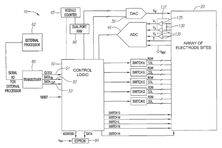
Turning now to the drawings, as shown in Fig. 3, an array-based electronic
chip 10 for carrying out and/or monitoring biologic reactions in accordance
with one
preferred form of the present invention comprises an array 20 of active
biologic
CA 02495426 2005-02-15
WO 2004/018991 PCT/US2003/025807
6
electrode sites 100. Coupled to the array 20 are a digital-to-analog converter
(DAC)
30, an analog-to-digital converter (ADC) 40, and a plurality of switch
controls, A, B,
C, D, E, G, M, L, N, and H.
The array-based chip 10 further includes a counter 65, e.g., a modulo 402
counter, a dual port random access memory module (RAM) 80, and an electrically
eraseable programmable read only memoxy module (EEPROM) 90 coupled to a
control logic module 50, which, in turn, is coupled to the DAC 30, the ADC 40,
and
switch controls (A-E, G, M, L, N, and H). In a preferred embodiment, each of
the
above listed elements may be disposed on a single semiconductor chip, and the
entire
chip 10 may be fabricated using conventional CMOS semiconductor fabrication
techniques. Further details on the fabrication techniques, which may be
employed in
making the chip 10, are disclosed in LT.S. Patent No. 6,258,606 issued to
Kovacs,
which is hereby incorporated by reference in its entirety.
Further, in the presently preferred form, an external processor 62, such as a
computer, may be used to interface with the chip 10; Preferably, the external
processor 62 may communicate with the chip 10 serially, using a transceiver 60
that
enables synchronous communication with the control logic module 50. The
communication interface between the transceiver 60 and the control logic
module 50
includes three signals: data-in 52, data-out 53, and a clock signal 51, which
may come
from the external processor 62.
Turning now to Fig. 4, the array 20 includes an array of individual biologic
electrode sites 100. Each electrode site 100 includes a working electrode W
coupled
with a sample-and-hold circuit 102, which may include five switches, A(n),
B(n),
C(n), D(n), and E(n) (n identifies a particular electrode site 100) a
capacitor 70, and
an operational amplifier 80. The switch controls A, B, C, D, and E shown in
Fig. 3
may be respectively coupled with each of switches A(n), B(n), C(n), D(n), an
E(n) via
row and column signal lines coupled to row and column decoders (not shown) to
enable the switches to be controlled individually. Preferably, array 20 is
further
coupled with a measurement circuit 137 comprising an external resistor 130 and
two
nodes coupled with two voltage sense amplifiers 135 for voltage measurements,
Vl
and VZ.
CA 02495426 2005-02-15
WO 2004/018991 PCT/US2003/025807
Still refernng to Fig. 3, in addition to the array of biologic electrode sites
100,
the array 20 may further include two dump circuits 95, 115, namely a short
dump
circuit 95 and a long dump circuit 115. The short dump circuit 95 preferably
includes
switches A(short), G, and M, a capacitor 90, an operational amplifier 140, and
a short
dump electrode DS. The long dump circuit 115 may include switches A(long), L,
and
N, a capacitor 110, an operational amplifier 150, and a long dump electrode
Dl. The
short 95 and/or long dump circuits I 15 may further be coupled with a
reference
electrode R, via a switch H (reference electrode R is shown in Fig. 3 only
coupled to
the long dump circuit 115). An external reference voltage source, Vref, is
preferably
applied to the reference electrode R, which may also be coupled to a voltage
sense
amplifier 13 S that provides a voltage measurement node, V3. Switches G, M, L,
N,
and H may be controlled by the control logic module 50 shown in Fig. 3. The
array
also preferably includes a temperature sensor 139, which provides a
temperature
measurement T of the solution containing biologic material.
15 Generally, each electrode site 100 and dump circuit 95, 115 operates in two
states, a sample state and a hold state. When a particular electrode site (n)
100 or
dump circuit 95, 115 is in a sample state, switch A(n, short, or long) closes,
and the
voltage, VW, supplied by the DAC 30 is applied to the capacitor 70, 90, 110
until the
capacitor 70, 90, 110 charges to a level that supplies a desired amount of
voltage to
20 the operational amplifier 80, 140, 150. Then, the electrode site (n) 100 or
dump
circuit 95, 115 changes to a hold state, where switch A(n, short, or long)
opens, and
the voltage applied to the noninverting input terminal(+)of the amplifier 80,
140, I50
is thus supplied by the capacitor 70, 90, 110. The capacitor 70, 90, 110 is
preferably
of a size, e.g., approximately 20 pF, that can quickly acquire the desired
charge when
switch A(n, short, or long) closes and hold the charge for a sufficient amount
of time
when switch A(n, short, or long) opens. As will be described below in more
detail,
during operation of the chip 10, the charge in each capacitor 70, 90, 110 is
refreshed,
i.e., recharged, preferably once approximately every 40.2 psec.
Additionally, the electrode sites 100 preferably operate in a variety of
modes,
e.g., normal mode, high-impedance mode, current measurement mode, and voltage
measuxement mode. Turning to Fig. 5(a), an electrode site 100 is setup to
operate in
normal mode, wherein a desired voltage is applied to the working electrode W.
This
CA 02495426 2005-02-15
WO 2004/018991 PCT/US2003/025807
mode is commonly referred to as "wet" mode because a solution is applied to
the
surface of the chip 10 containing the working electrodes W. Switches B(n) and
D(n)
form a closed circuit with the working electrode W, i.e., positioned such that
the
output of the operational amplifier 80 is applied to the working electrode W
(i.e., to
drive the working electrode W) and then fed back to inverting input terminal (-
) of the
operational amplifier 80. Switches C(n) and E(n) are open during normal mode.
Turning to Fig. 5(b), the electrode site 100 is shown configured in high-
impedance mode, which effectively isolates the working electrode W from the
array
20. In this mode, switches B(n) and D(n) form open circuits with the working
electrode W, i.e., positioned such that the output of the operational
amplifier 80
bypasses the working electrode W. Switches C(n) and E(n) are open during high-
impedance mode.
Turning to Fig. 5(c), the electrode site 100 is configured in current
measurement mode, wherein the current through the working electrode W may be
measured. Switch B(n) forms an open circuit with the working electrode W.
Switch
D(n) forms a closed circuit with the working electrode W. Both switches C(n)
and
E(n) are closed, creating a circuit loop with the measurement circuit 137,
i.e., a circuit
loop is created through the external xesistor 130, which is preferably a
precision
resistor, the working electrode W, and the operational amplifier 80. The
current
through the working electrode W may be calculated by subtracting V 1 from V2,
the
outputs of the voltage sense amplifiers 135, and dividing the difference by
the
external resistor 130 in accordance with Ohm's law, i.e., (Vl-VZ)1(Resistor
130). The
resistor 130 is preferably approximately 385 kSZ.
Turning to Fig. 5(d), the electrode site 100 is set up in voltage measurement
mode, wherein the voltage applied to the working electrode W may be measured
and
tested. The configuration is similar to normal mode shown in Fig. 5(a), except
that
switch E(n) is closed. Thus, the voltage applied at the working electrode W
can be
measured at V2. In addition to being able to measure the working electrode W
voltage
VZ with solution applied, this mode of operation also allows dry test
capability, i.e.,
the electrodes W, D and R may be tested before a solution is placed over the
array 20.
In this regard, the integrity of the chip 10 can be tested at the
manufacturing facility
much earlier in the manufacturing process than prior devices.
CA 02495426 2005-02-15
WO 2004/018991 PCT/US2003/025807
9
Turning to Fig. 5(e), the electrode site 100 is configured in current
measurement mode coupled with an alternative measurement circuit 138, which
includes a transconductance amplifier 200. The noninverting input terminal (+)
of the
amplifier 200 is coupled with switch C(n), which is closed. The inverting
input
terminal (-) and the output of the amplifier 200 are coupled with switch E(n),
which is
also closed.
The amplifier 200 outputs a current, IW, which represents the current through
the working electrode W. However, Iw may include parasitic noise caused by the
sample-and-hold circuits of the electrode sites 100. Because the amplifier 200
outputs
a current, the impedance of the amplifier 200 is high, which, as can be
appreciated by
one of ordinary skill in the art, allows the output current to be accurately
copied with
reduced parasitic noise. Thus, to reduce the parasitic noise of IW, the
amplifier 200
produces a copied version Io"t. Iout is passed through a resistor 205, which
may be
coupled with a ground or an external voltage source, e.g., a voltage source
Vref of
2.5V. In accordance with Ohm's law, the current IW may be calculated by
subtracting
Vl by the voltage source, e.g., a Vref of 2.5V, and dividing the difference by
the value
of the resistor 205. The resistor 205 is preferably approximately 385 kS2.
Turning to Fig. 5(f), an electrode site 100 is shoran coupled with measurement
circuit 138. The electrode site 100 is configured in voltage measurement mode,
wherein the voltage of the working electrode W may be measured. The
configuration
is similar to the configuration of the normal mode, as shown in Fig. 5(a),
except that
switch E(n) is closed, thus closing the circuit with the node at V2. The
voltage at VZ
represents the voltage of the working electrode W.
As mentioned above, in addition to the array of electrode sites 100, the array
20 may include dump circuits 95, 115, such as the short dump circuit 95 and
long
dump circuit 115 shown in Fig. 4. During operation of the sample-and-hold
circuits
of the electrode sites 100, there are some situations where it may be
desirable to have
a reference node shorted to ground. In other situations, it may be desirable
to
maintain a reference node at a voltage level other than ground. In these other
situations, one approach is to couple the reference node to a dump circuit
having a
potential other than ground.
CA 02495426 2005-02-15
WO 2004/018991 PCT/US2003/025807
One possible situation, for example, is when measuring the current of the
working electrode W using the current measurement circuit 138, described above
and
shown in Fig. 5(e). During operation, the voltage V1 may switch between a
first and
second value. If the resistor 205 was coupled to a reference node that was
shorted to
ground, then the measured current, i.e., VI divided by the resistor 205, may
oscillate
between a higher current and a lower current. If the reference mode was set to
a
voltage approximately in between the first and second value, then the measured
voltage Vl of the electrode may switch between a negative value and a positive
value,
which in turn results in a current measurement that switches between a
negative value
10 and a positive value.
As can be appreciated by one of ordinary skill in the art, this advantageously
allows the working electrodes W to function as "counter-electrodes" for each
other.
In other words, if the current of a working electrode W is flowing in one
direction,
e.g., a positive current, a circuit may be completed by coupling the working
electrode
1 S W with another working electrode W having a current flowing in the
opposite
direction, e.g., a negative current.
The operation of the dump circuits 95, 115 are similar to the electrode sites
100. If, for example, the use of a short dump circuit 9S is desired, switch
A(short)
may close so that VW from the DAC 30 may charge capacitor 90. When charged,
the
capacitor 90 supplies a voltage to the noninverting input terminal (+) of
operational
amplifier 140. The output of the operational amplifier 140 is fed back into
the
inverting input terminal (-) of the operation amplifier 140. Additionally,
switches G
and M may be closed so the voltage output of the operational amplifier 140 may
be
applied to the dump electrode DS, which may be coupled with the desired
electrode
sites) 100.
Similarly, if the use of the long dump circuit 11 S is desired, switch Along)
may close so that VW from the DAC 30 may charge capacitor 110. When charged,
the
capacitor 110 supplies a voltage to the noninverting input terminal (+) of
operational
amplifier 1 S0. The output of the operational amplifier 1 SO is fed back into
the
inverting input terminal (-) of the operational amplifier 150. Additionally,
switches L
and N may be closed so the voltage output of the operational amplifier 150 may
be
CA 02495426 2005-02-15
WO 2004/018991 PCT/US2003/025807
11
applied to the dump electrode Di, which also may be coupled with the desired
electrode sites) 100.
As mentioned above, the control logic module 50 may control the state and the
modes of operation of the electrode sites 100 individually. Further, the
control logic
module 50 may also control the dump circuits 95, 115 by controlling switches
G, M,
L, N, and H.
Turning now to methods of delivering electrical stimuli to the working
electrodes W, there are preferably at least three methods: constant voltage,
constant
current, and voltage reference. The constant voltage method involves applying
a
desired constant voltage to the working electrode W. In contrast, the constant
current
method involves applying a desired constant current to the working electrode
W.
The voltage reference method involves maintaining a user programmable
offset between a working electrode W and a reference voltage source Vref~ The
voltage source Vref may be coupled with the array 20 via a reference electrode
R. Fig.
4 shows Vref coupled with a reference electrode R that is coupled with the
long dump
circuit 115 via switch H, however Vrefmay be coupled with the array at other
locations, for example, with the short dump circuit 95. The voltage of the
reference
electrode R may be monitored using a sensor amplifier 135 (represented as V3
in Fig.
4). Preferably, the reference electrode R is located in the flow cell
(discussed in more
detail below) that is fornled in connection with the chip 10.
The array-based electronic chip 10 may also control the delivery method of the
electrical stimuli to each working electrode W and the dump circuits 95, 115,
individually or in selected groups. To control the delivery of the electrical
stimuli, the
chip 10, using the DAC 30, sets voltage VW, which is coupled to the electrode
sites
100 and the dump circuits. The DAC 30 retrieves the desired VW value from the
dual
port RAM 80 and the control logic module 50. For an array 20 that has 400
electrode
sites 100, a short dump circuit 95, and a long dump circuit 115, the RAM 80
may
have 402 bytes of data. Each byte corresponds to an electrode site 100 or a
dump
circuit 95, 115 and represents a specific voltage for V«,.
The chip 10 charges each electrode site 100 and dump circuit 95, 115
sequentially, controlled by the counter 65. The counter 65 specifies the byte
(n)
within the RAM 80 that the DAC retrieves to set V,~. While the DAC 30 is
retrieving
CA 02495426 2005-02-15
WO 2004/018991 PCT/US2003/025807
12
the voltage value and setting VW, the control logic 50 reads the module
counter 65 and
sets the corresponding electrode site 100 or dump circuit 95, 115 into the
sample state,
i.e., the control logic module 50 closes switch A(n) for the corresponding
electrode
site (n) 100 or dump circuit 95, 115. When the corresponding capacitors) 70,
90, 110
charges, the control logic module 50 changes the electrode site (n) 100 or
dump
circuit 95, 115 to a hold state, i.e., opens switch A(n).
The module counter 65 then increments to the next byte within the RAM 80,
i.e., (n+1), and the DAC 30 reads the voltage value in the next byte (n+1) to
set VW.
While the DAC 30 is retrieving the voltage value of byte (n+1) and setting VW,
the
control logic 50 reads the counter 65 and sets the next electrode site (n+1)
100 or
dump circuit 95, 115 into the sample state, i.e., the control logic module 50
closes
switch A(n+1). When capacitor 70, 90, 110 charges, then the control logic
module 50
opens switch A(n+1).
This process is known as "refreshing" the electrodes, and the process cycles
through the sample-and-hold circuits 102 and dump circuits 95, 115
sequentially
during operation. Timing is critical because the refreshing process must be
fast
enough to maintain the desired charges on the capacitors, 70, 90, 110, before
they
deplete to undesirable levels, but each circuit must maintain a sample state
long
enough for the respective capacitor, 70, 90, 110, to charge to the desired
level. Using
a dual port RAM 80 allows the counter 65 and the DAC 30 to access the RAM 80
simultaneously, which improves the timing of the chip 10. Preferably, the DAC
30
and the counter 65 are driven by a clock signal of approximately 10 MHz.
When the delivers electrical stimuli;to a particular working electrode W via
the constant voltage method, the desired voltage is applied via VW, as
described
above. The desired voltage may be either a single voltage value or a
programmed
series of different voltage values, such as positive and negative voltages
values. To
maintain the desired constant voltage, the control logic module 50 may set the
electrode site 100 of the particular working electrode W to voltage
measurement
mode. Thus, the voltage of the working electrode VZ may be monitored. The
measurement at VZ may be fed into the ADC 40 to convert the measurement into a
digital value. The control logic module 50 may then retrieve the working
electrode W
voltage VZ from the ADC 40 to compare with the desired constant voltage. If VZ
is
CA 02495426 2005-02-15
WO 2004/018991 PCT/US2003/025807
13
too high or too low, then the control logic module 50 may accordingly adjust
the
value for VW set in the RAM 80 for the corresponding electrode site 100.
When the chip 10 delivers electrical stimuli via the constant current method,
the desired voltage Vw is applied to produce the desired constant current
through the
working electrode W, as described above. The desired constant current may be
either
a single value or a programmed series of different current values, such as
positive and
negative current values. To maintain the constant current, the control logic
module 50
sets the corresponding electrode site 100 to current measurement mode and then
monitors the current by retrieving data, such as Vl andlor VZ, from the ADC 40
and
calculating the current, as described above. If the current is too high or too
low, the
control logic 50 may accordingly adjust the VW
When the chip 10 deliveis electrical stimuli via the voltage reference method,
the desired VW is applied such that the voltage at the working electrode W is
offset
from Vref bY a user programmable amount. The programmed offset may be either a
single value or a series of different values, such as positive and negative
values. To
maintain the user programmable offset, the control logic module 50 sets the
particular
electrode site 100 to dry voltage test mode and then compares VZ with V3, the
voltage
of the reference electrode R that is coupled with Vref. If the offset is too
much or too
little, the control logic module 50 may accordingly adjust VW, as described
above.
The control logic module 50 also includes a reset signal, which, when
invoked, refreshes the electrodes sites 100 and the dump circuits 95, 115
starting from
the first electrode site 100, i.e., the counter 65 is reset to 0.
In addition, the control logic module 50 may monitor the temperature of the
array 20 via the temperature sensor module 139.
As mentioned above, the chip 10 further includes an EEPROM 90 coupled
with the control logic module 50. This allows the control logic module 50 to
store
extra data associated with the array 20, e.g., calibration data for the
temperature
sensor 139. The EEPROM 90 is read/write, but the data may be changed by
"powering up" the EEPROM 90 only. This may be achieved by applying
approximately 20V to Vpp and performing a write.
Turning now to a description of the interface with the chip 10 and more
specifically with the control logic module 50, the interface is a three wire
serial
CA 02495426 2005-02-15
WO 2004/018991 PCT/US2003/025807
14
interface which includes data-in 52, data-out 53, and clock 51, as shown in
Fig. 3.
Although data-in 52 and data-out 53 are separate, the interface is half
duplex, i.e., a
response coming from the chip 10 occurs only after a command from the external
processor 62 has been fully received. The interface is synchronously driven by
the
clock 51, preferably at 10 MHz. Preferably, there is a two clock cycle delay
between
data-in 52 and data-out 53. The data-in 52 signal is a 24-bit message which
includes:
a start bit, a 12-bit address, a 1-bit command, an 8 bit data field, and two
stop bits.
The 12-bit address may represent, for example, the individual switches
controls, A, B, C, D, E, G, M, L, N, H, the DAC 30 controls, the data to be
written to
either the EEPROM 90 or the RAM 80, e.g., voltage values for VW when the DAC
30
refreshes the electrode sites 100, the ADC 40 controls, temperature sensor 139
controls.
The 1-bit command may indicate whether the external processor 62 intends to
read data from the chip 10 or write data to the chip 10, e.g., write to the
RAM 80 or
EEPROM 90 or control the switches.
The data-out signal is an 11-bit message produced by the control logic module
50 if the 1-bit command in data-in is a read command. The data-out signal
includes: a
start bit, an 8-bit data field, and two stop bits. The 8-bit data field may
include, for
example, the status of the switches, i.e., whether the switch is open or
closed and/or
data from the RAM 80, EEPROM 90, and/or ADC 40, which may include data from
Vn Vz~ Vs~ Vref~ and/or T.
Turning to Fig. 6, a preferred die 300 layout of an embodiment of the present
invention is shown. The die 300 is preferably approximately 8mm by Smm. 400
working electrodes W of the array 20 are shown in a matrix of 16 rows and 25
columns. However, an embodiment of the present invention may include any
number
of working electrodes W. The electrodes W are preferably approximately 50
microns
in diameter on 150 micron centers. In addition, the working electrodes W are
preferably comprised of platinum or platinum silicide and are preferably
planar.
The long dump electrodes Dl and the short dump electrodes DS are also shown
along the perimeter of the working electrodes W. Around the perimeter of the
layout
are bond pads 305 for chip related functions. It should be noted that in this
particular
layout, the reference electrode R is not shown. In a preferred form, the
reference
CA 02495426 2005-02-15
WO 2004/018991 PCT/US2003/025807
electrode is comprised of silvex, and thus xesides off the die 300, preferably
in the
flow cell 230. The reference electrode R may be coupled to the array 20 via
the bond
pads. The remaining elements of the chip 10 reside within the die 300.
Preferably, the chip 10 may be designed such that there is less than 10%
5 electrode currant variation from 630 nm light incident at 10 mw/mm2. An
optical
block (not shown) may be placed in the top of the metallization layer of the
electrodes
W to help resolve this issue. Optionally, there may be four electrode size
areas (not
shown) in between the dump circuits 95, I 15 and the array of electrode sites
100
towards the c;o~rner of the die :300 coaied with a fluorescent material to be
used as an
10 optical standard.
Turning to Fig. 7(a), the die 300 is shown installed in a cartridge 225 used
io
apply a solution to the working electxodes W and more readily couple the chip
10
with an external processor 62. The cartridge 225 includes a flow cell 230 thai
acts as
a chamber over the die 300.that contains the solution containing charged
biological
15 material. Injection ports 220 are placed on both sides of the die 300. The
solution
eniers ono port 220, floods over the working electrodes W, and exits the other
port
220.
Turning to Fig. 7(b), the flip-side of the cartridge 225 and the die 300 is
sho~un. Thc; cartridge 22 5 further includes pins within the die 300 to
electrically
corme~:.t certain elerxier~.is within the array-based chip 10 to external
components. The:
Vpp pin is for coupling a power supply of approximately 20V vaith the
EEPROI',~I 90.
The D'.~a pin is for coupling the arxay-based chip 10 with a digital powex
supply of
approximatety 5V, and the :~~~dd pin is for coupling the chip 10 with ar
analog po~~jex
supply of approxirrxately SV~. T he Reset pin is for coupling a reset signal.
to the
control logic: module 50.
The data-out 53; data-in 52, and clock 51 pins are for interfacing with the
external processor 62, which may be via a transceiver 60. The Rl arid R2 pins
are for
coupling each end of an. external resistor, e.g., resistor 130, to the array
20. The A.~~$S
pin is for coupling the array 20 with an analog ground. and the I5vs5 is for
coupling the
array 20 with a digital ground. t~ chip-is-in-use pin provides a signal that
indic:~tes
whether the chip 10 is in operation.
CA 02495426 2005-02-15
WO 2004/018991 PCT/US2003/025807
16
While the invention is susceptible to various modifications, and alternative
forms, specific examples thereof have been shown in the drawings and are
herein
described in detail. It should be understood, however, that the invention is
not to be
limited to the particular forms or methods disclosed, but to the contrary, the
invention
is to cover all modifications, equivalents and alternatives falling within the
spirit and
scope of the appended claims.