Note: Descriptions are shown in the official language in which they were submitted.
CA 02495843 2005-02-17
WO 2004/022161 PCT/US2003/027524
OPTOELECTRONIC DEVICE FOR THE TREATMENT OF MUSCLE OR JOINT PAIN
This application claims priority under 35 U.S.C. ~119 to United States
Provisional
Patent Application No. 60/408,216 filed September 4, 2002, which is
incorporated by
reference herein.
BACKGROUND OF THE INVENTION
This invention was made with U.S. Government support under Contract DAAHO1-03-
C-R-120 awarded by the Defense Advanced Research Projects Agency (DARPA). The
U.S.
Government has certain rights in this invention.
This invention relates to a device for the treatment of muscle or joint pain.
The
device includes arrays of optoelectronic devices, such as light emitting
diodes, that emit
radiation suitable for the treatment of muscle or joint pain.
Biostimulation is a method of using monochromatic light to deliver photons to
cytochromes in the mitochondria of cells. Cytochromes are light-sensitive
organelles that act
as an electron transport chain, converting energy derived from the oxidation
of glucose into
adenosine triphosphate (ATP) - the mitochondria's fuel. By directly
stimulating
cytochromes with monochromatic light, it is believed that more fuel is pumped
into the
mitochondria of cells, increasing the energy available to the cells.
Increasing the energy
available to the cell is believed to help relieve pain.
By pumping more fuel into the mitochondria, biostimulation is believed to
increase
the respiratory metabolism of many types of cells. The monochromatic light
provided by
biostimulation is believed to be absorbed by the mitochondria of many types of
cells where it
stimulates energy metabolism in muscle and bone, as well as skin and
subcutaneous tissue.
Specifically, biostimulation is believed to result in fibroblast
proliferation, attachment and
synthesis of collagen, procollagen synthesis, macrophage stimulation, a
greater rate of
extracellular matrix production, and growth factor production. Specifically,
the growth
factors that are produced include keratinocyte growth factor (KGF),
transforming growth
factor (TGF), and platelet-derived growth factor (PDGF).
CA 02495843 2005-02-17
WO 2004/022161 PCT/US2003/027524
during the healing process. Specifically, these activities are believed to
include fibroblast
proliferation, growth factor synthesis, collagen production, and angiogenesis.
Using lasers to provide monochromatic light for biostimulation has several
disadvantages. First, lasers are limited by their wavelength capabilities.
Specifically, the
combined wavelengths of light optimal for treating muscle and joint pain
cannot be
efficiently produced, because laser conversion to near-infrared wavelengths is
inherently
costly. Second, lasers are limited by their beam width. A limited beam width
results in
limitations in the area which may be treated by lasers. Third, and most
importantly, along
with the production of monochromatic light, lasers produce a significant
amount of heat. As
a result of the production of heat, lasers cannot be used for extended
treatment times or in
applications in which the patient cannot tolerate heat.
SUMMARY OF THE INVENTION
The invention provides a device for treating a medical condition, such as
muscle or
joint pain, using an array of optoelectronic devices, such as light-emitting
diodes (LEDs). In
one embodiment of the invention, a device for treating muscle or joint pain is
a self
contained, self powered, hand-held device that can emit radiation having a
light intensity of
at least approximately 30 milliwatts per centimeter squared. The device
includes a housing, a
portable power source disposed in the housing, and one or more optoelectronic
devices
disposed in the housing and coupled to the portable power source. The device
also includes a
cooling system disposed in the housing. The cooling system can dissipate the
heat generated
by the optoelectronic devices.
According to one embodiment of the method of the invention, a user positions a
housing including optoelectronic devices adjacent to a muscle andlor a joint
of a patient. The
user irradiates the muscle and/or the joint with radiation emitted by the
optoelectronic
devices. The emitted radiation has a wavelength suitable for the treatment of
muscle and/or
joint pain. The heat produced by the optoelectronic devices is dissipated
through the housing.
According to another embodiment of the method of the invention, a user
positions a
housing adjacent to at least one of a muscle and a joint of a patient. A
plurality of
optoelectronic devices are disposed in the housing. The user irradiates the
muscle and/or the
joint with radiation emitted by the plurality of optoelectronic devices for a
treatment session
having a first duration. The plurality of optoelectronic devices are allowed
to dissipate heat
2
CA 02495843 2005-02-17
WO 2004/022161 PCT/US2003/027524
for a cooling-down period having a second duration, and the plurality of
optoelectronic
devices are prevented from emitting radiation during the cooling-down period.
BRIEF DESCRIPTION OF THE DRAWINGS
These and other features of the present invention will be apparent to those
skilled in
the art from the following description of the preferred embodiments and the
drawings, in
which:
FIG. 1 is a top perspective view of a hand-held device according to one
embodiment
of the present invention.
FIG. 2 is a bottom perspective view of the hand-held device of FIG. 1.
FIG. 3 is a side elevational view of the hand-held device of FIG. 1.
FIG. 4 is a side elevational view of the hand-held device of FIG. 1 with a
power
source compartment cover removed.
FIG. 5 is an exploded side elevational view of the hand-held device of FIG. 1.
FIG. 6 is a perspective view of a heat sink, a circuit board, and a ceramic
assembly of
the hand-held device of FIG. 1.
FIG. 7 is a side elevational view of the heat sink, the circuit board, and the
ceramic
assembly of FIG. 6.
FIG. 8 is a side elevational view of the heat sink and the ceramic assembly
of~FIG. 6.
FIG. 9 is a side elevational view of the heat sink and the circuit board of
FIG. 6.
FIG. 10 is a schematic diagram of a control circuit for use with the hand-held
device
of FIG. 1.
FIG. 11 is a current source module of the control circuit of FIG. 10.
FIG. 12 is a voltage reference module of the control circuit of FIG. 10.
FIG. 13 is a power control module of the control circuit of FIG. 10.
3
CA 02495843 2005-02-17
WO 2004/022161 PCT/US2003/027524
FIG. 14 is a power-on reset module of the control circuit of FIG. 10.
FIG. 15 is a temperature sensing module of the control circuit of FIG. 10.
FIG. 16 is a battery voltage sensing module of the control circuit of FIG. 10.
DETAILED DESCRIPTION
In each of the embodiments of the present invention, at least one
optoelectronic
device is used to emit radiation for the treatment of a medical condition,
such as for the
treatment or relief of muscle or joint pain. The optoelectronic devices can be
substantially
monochromatic, double-heterojunction, Gallium-Aluminum-Arsenide (GaAIAs) LEDs
of the
type manufactured by Showa Denkoa or Stanley, both of Japan, or by Hewlett-
Packard of
Palo Alto, California. In some embodiments, the optoelectronic devices are
connected
together in a manner described in U.S. Patent No. 5,278,432 issued January 1
l, 1994 to
Ignatius et al., which is incorporated herein by reference.
In some embodiments, the LEDs emit radiation at approximately 670 nanometers
(nm) +/- approximately 1 S nm, which is believed to be an optimal wavelength
for relieving
and potentially treating muscle and/or joint pain. Some embodiments of the
invention
include an array of LEDs that emit radiation. Other wavelengths may also be
suitable for
relieving and treating muscle and/or joint pain or for treating other medical
conditions, such
as approximately 300 nm to 950 nm, and more specifically, approximately 640 nm
to 700
nm. Moreover, as further research is conducted, other wavelengths may be found
to be
effective. However, the present invention is not limited to the use of any
specific
wavelength. In some embodiments, the LEDs are wavelength specific in that the
LEDs emit
a certain wavelength when provided with power. For example, one or more
wavelength-
specific LEDs emitting radiation at 670 nm can be assembled onto a circuit
board or any
other suitable substrate in order to provide a hand-held device 10 that emits
radiation at a
central wavelength of 670 nm.
In addition to the wavelength of the radiation emitted by the LEDs, the
following
parameters should be considered to optimize the stimulative effect of the LEDs
on biological
tissues: the energy density required for activation (Ela)s~l, the light
intensity Istt~", and the
total irradiation time Ot~o~. The parameters are interrelated according to the
following
equation,
4
CA 02495843 2005-02-17
WO 2004/022161 PCT/US2003/027524
(E/a)act - Istim x ~ttot
where intensities necessary for stimulation Istim should surpass a threshold
intensity Io, i.e.,
Istim ~ Io .
Light intensities lower than threshold values to typically may not produce
biostimulatory
effects, even under prolonged irradiation times ~t~o~.
It is believed that the optimal energy densities for cellular activation
(Ela)~~t are
approximately 4 to 8 Joules per centimeter squared. The light intensity
(Isl"n) of the radiation
emitted by the LEDs may be approximately 30 to 80 milliwatts (mW) per
centimeter squared,
and up to approximately 200 milliwatts per centimeter squared. In one
embodiment, the
LEDs emit radiation at an intensity of approximately 50-60 milliwatts per
centimeter squared.
In some embodiments, the irradiation time Ottot per treatment period is about
88 seconds +l- 8
seconds.
In some embodiments, the LEDs emit radiation having a relatively constant
light
intensity over a treatment area. In one embodiment, the light intensity varies
by less than
about 30% over a treatment area of approximately ten square centimeters. For
example, 4.8
LEDs per centimeter squared for a total of 48 LEDs can provide a relatively
constant light
intensity over a treatment area of approximately ten square centimeters.
However, fewer than
4.8 LEDs per centimeter squared can be used if the LEDs emit radiation at a
higher light
intensity.
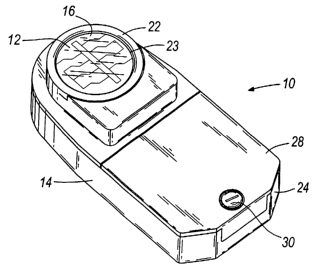
FIGS. 1 and 2 illustrate a hand-held device 10 according to one embodiment of
the
invention. As shown in FIG. 2, the hand-held device 10 includes one or more
LEDs 12 (e.g.,
an array of LEDs) that can emit radiation toward a patient. The hand-held
device 10 includes
a housing 14 that supports the LEDs 12. The housing 14 can be constructed of a
polycarbonate ABS alloy or any other suitable packaging polymer. In some
embodiments,
the housing 14 provides a sealed, self contained enclosure for the hand-held
device 10 so that
no contaminates can enter the hand-held device 10. In other embodiments, the
housing 14
includes vents so that air can pass through the housing 14 to cool the LEDs 12
or so that a fan
(not shown) can be included in the housing 14 to cool the LEDs 12. If a fan is
included in the
housing 14, the hand-held device 10 can be powered by a portable power source
within the
housing 14 or by an AC power source (e.g., a power cord, a transformer, andlor
an electrical
5
CA 02495843 2005-02-17
WO 2004/022161 PCT/US2003/027524
plug for connection to a wall outlet). In some embodiments, a fan can provide
continuous
cooling, without a cooling-down period in which the LEDs 12 cannot be
illuminated. A heat
sinle having fins (not shown) can also be used in conjunction with a fan to
cool the LEDs 12.
As also shown in FIG. 2, the hand-held device 10 can include a cover plate 16
suitable
to electrically isolate the patient from the LEDs 12. The cover plate 16 can
be constructed of
any suitable transparent or semi-transparent material. As shown in FIG. 1, the
housing 14
can include one or more user-manipulatable controls 18 (e.g., a START button
and a STOP
button) and one or more indicator lights 20 (e.g., a LOW BATTERY light and a
DELAY
light).
As shown in FIG. 3, the housing 14 can include a raised portion 22 within
which the
LEDs 12 can be positioned. The raised portion 22 can include a circular
aperture 23 (as
shown in FIG. 2), or an aperture having any other suitable shape, through
which the LEDs 12
can emit radiation. The cover plate 16 can be positioned within the raised
portion 22 over the
LEDs 12. The cover plate 16 can be coupled to the raised portion 22 with an
ultraviolet
epoxy or with any other suitable adhesive or fastener.
As shown in FIGS. 1 and 5, the housing 14 can include a top cover 24 and a
bottom or
aperture cover 26. The bottom cover 26 can include or can be coupled to the
raised portion
22. As shown in FIGS. 4 and 5, the housing 14 can include a power source
compartment
cover 28 removably coupled adjacent to the bottom cover 26 with a screw 30.
The hand-held
device 10 can be powered by any suitable power source, including rechargeable
or non-
rechargeable, standard or non-standard batteries; AC power sources or
connections; fuel
cells; and other portable power sources. In one embodiment, the power source
is eight
standard AA-sized batteries which can be held together within the housing 14
by a battery
holder.
As shown in FIG. 5, the hand-held device 10 can include a cooling system in
the form
of a heat sink 32. The heat sink 32 can be constructed of aluminum, an
aluminum alloy, or
any other material suitable for dissipating heat. The heat sink 32 can have a
total mass
suitable for dissipating heat from the LEDs 12 during a cooling-down period of
a reasonable
duration (e.g., approximately 88 seconds after a single treatment session or
several seconds
longer after more than one consecutive treatment session). In one embodiment,
the total mass
of the heat sink 32 allows the hand-held device 10 to operate for eight to ten
treatment
6
CA 02495843 2005-02-17
WO 2004/022161 PCT/US2003/027524
sessions before the cooling-down period of 88 seconds must be extended (as
will be
described below with respect to FIGS. 10-16). The total mass of the heat sink
32 can also be
designed so that the total weight of the hand-held device 10 (preferably
including the
batteries or other portable power source) is about one pound.
The heat sink 32 can be coupled to a first side 33 of a ceramic assembly 34 by
one or
more screws 38 (e.g., three nylon screws) or by a suitable thermal adhesive.
The LEDs 12
(e.g., an array of several LEDs) can be coupled to a second side 35 of the
ceramic assembly
34. The ceramic assembly 34 is thermally conductive in order to transfer heat
emitted by the
LEDs 12 to the heat sink 32, but the ceramic assembly 34 is not electrically
conductive.
In other embodiments, the cooling system of the hand-held device 10 can
include a
thin-film insulator (not shown) coupled to an aluminum substrate (not shown).
A suitable
thin-film insulator is Kapton~ manufactured by E. I. Du Pont De Nemours and
Company
Corporation.
As shown in FIG. 5, the heat sink 32 can also be coupled to a circuit board 36
by any
suitable fasteners, such as screws 39 positioned through holes 41 in the
circuit board 36. The
heat sink 32 can include one or more elevated portions (or bosses or stand-
offs) 37 that
closely or directly contact one or more components mounted on the circuit
board 36 (e.g., a
temperature sensor and/or various transistors, as are described below with
respect to FIGS.
10-16) in order to dissipate heat from those particular components. The
elevated portions 37
can also create an air gap between the heat sink 32 and the circuit board 36
to further cool the
components mounted on the circuit board 36. The elevated portions 37 can be
integrally
molded with the heat sink 32. The circuit board 36 can be connected to the
LEDs 12 by a
conductor jumper 40 (e.g., a twelve-conductor jumper in one embodiment or by
two or more
wires or groups or wires in other embodiments). The circuit board 36 can be
connected to
one or more batteries (not shown) or to any other suitable power source by a
positive
connection 43 (e.g., VBatt) and can be grounded with a ground wire 45 (as
shown in FIG. 9).
The positive connection 43 can be connected to one or more battery clips 42.
The battery
clips 42 can be attached to a partition wall 44 included in or coupled to the
bottom cover 26.
In some embodiments, when batteries are inserted into the housing 14, the
battery clips 42
connect the positive ends of the batteries to the positive connection 43.
7
CA 02495843 2005-02-17
WO 2004/022161 PCT/US2003/027524
As also shown in FIG. 5, the bottom cover 26 can include one or more heat sink
support members 46. The heat sink support members 46 can be positioned within
corresponding recesses 48 on the edges of the heat sink 32. The top cover 24
of the housing
14, the bottom cover 26 of the housing 14, the heat sink 32, the ceramic
assembly 34, and the
circuit board 36 can be secured to one another by one or more suitable
fasteners (e.g., screws
50), by suitable adhesives, or by a combination of fasteners and adhesives.
FIGS. 6 and 7 illustrate the LEDs 12, the heat sink 32, the ceramic assembly
34, and
the circuit board 36 as assembled, but not positioned inside of the top cover
24 and the
bottom cover 26 of the housing 14. FIG. 7 also illustrates a push button 52
coupled to the
circuit board 36 (only one push button is shown from the side elevational
view, although
some embodiments include two push buttons for the two user-manipulatable
controls 18
shown in FIG. 1). In addition, FIG. 7 illustrates an indicator light 54 (only
one indicator light
is shown from the side elevational view, although some embodiments include two
indicator
lights for the two indicator lights 20 shown in FIG. 1). FIG. 8 illustrates
the LEDs 12
coupled to the ceramic assembly 34 and the heat sink 32. FIG. 9 illustrates
the circuit board
36 coupled to the heat sink 32.
In some embodiments, the hand-held device 10 does not include a cooling system
(i.e., no heat sink or fan). In these embodiments, the LEDs 12 are mounted to
the circuit
board 36 which is positioned inside of the housing 14. The LEDs 12 can be
allowed to emit
as much heat as possible without an additional cooling system.
FIG. 10 is a schematic diagram of a control circuit 100 for use with the hand-
held
device 10. The components and connections of the control circuit 100 can be
included in
and/or mounted to the circuit board 36 described above. The control circuit
100 can include a
current source module 102 that drives the LEDs 12 (via connections M through
T). The
current source module 102 can be connected to a voltage reference module 104
(via a
connection A). The voltage reference module 104 can be connected to a battery
voltage
sensing module 106 (via connections C and D), a temperature sensing module 108
(via
connections B and E), and a power-on reset module 110 (via a connection F).
The power-on
reset module 110 can be connected to a power control module 112 (via a
connection G). The
battery voltage sensing module 106 can be connected to the power control
module 112 (via a
connection H). The power control module 112 can be connected to the LEDs 12
(via a
connection I). The temperature sensing module 108 can be connected to the
power-on reset
CA 02495843 2005-02-17
WO 2004/022161 PCT/US2003/027524
module 110 (via a connection J). The battery voltage sensing module 106 can be
connected
to the power-on reset module 110 (via a connection I~) and to the temperature
sensing
module 108 (via a connection L). Particular embodiments of each of these
modules will be
described in detail with respect to FIGS. 11-16.
S FIG. 11 illustrates one embodiment of the current source module 102. The
current
source module 102 can include eight current sources 114 resulting in eight
channels being
connected to the LEDs 12 (via connections M through T) in order to provide
eight control
signals or driving currents to the LEDs 12. In one embodiment, each channel is
connected to
six LEDs (e.g., two parallel strings of three LEDs in each string) for a total
of 48 LEDs. In
other embodiments, the LEDs 12 can be connected in any suitable manner, such
as all of the
LEDs being connected in series or all of the LEDs being connected in parallel,
or any other
combination of strings of LEDs being connected in series and in parallel. In
some
embodiments, any number of LEDs 12 can be connected in any manner as long as
all of the
LEDs can be turned ON and turned OFF at the same time. As shown in FIG. 10,
each set of
six LEDs can be connected to a positive power source V+ (via the connection I)
from the
power control module 112. The current sources 114 can provide approximately 98
milliamps
to the LEDs 12 connected to each one of the eight channels and approximately
49 milliamps
to each string of three LEDs. Each one of the current sources 114 can include
an operational
amplifier 116. In one embodiment, two quad operational amplifiers can be used
for the eight
current sources 114 (a first quad operational amplifier includes U9A-U9D and a
second quad
operational amplifier includes UlOA-UlOD). Suitable operational amplifiers are
Model No.
LM324 operational amplifiers manufactured by National Semiconductor.
The output of each operational amplifier 116 can be connected to the gate of a
transistor 118 (Q8-Q15). The drain of the transistor 118 can be connected to
one set of six
LEDs 12. Suitable transistors are Model No. TN0104 n-channel MOSFET
transistors
manufactured by Supertex. In each current source 114, a sensing resistor 120
(e.g., 5 Ohm
resistors R20-R27) can be connected to a first input of the operational
amplifier 116 and to
the source of the transistor 118. The transistor 118 acts as a switch between
the LEDs 12 and
the positive power source V+ from the power control module 112. The sensing
resistor 120
can determine how much current is being provided to the transistor 118 and the
LEDs 12 at a
test point (TP8-TP15). A second input of the operational amplifier 116 can be
connected to a
9
CA 02495843 2005-02-17
WO 2004/022161 PCT/US2003/027524
common node or test point TPS in the voltage reference module 104 (at
connection A as
shown in FIG. 12).
Referring to FIGS. 11 and 12, the voltage at test point TPS provides a
reference
voltage to each one of the current sources 114. In some embodiments, the test
point TPS
reference voltage is approximately 0.49 Volts in order to provide 98 milliamps
to each one of
the current sources 114 (i.e., 98 milliamps to each set of six LEDs and 49
milliamps to each
string of three LEDs). FIG. 12 illustrates one embodiment of the voltage
reference module
104. Two resistors R18 (e.g., 1.5 kilo-ohms) and R19 (e.g., 1 kilo-ohm) can
form a voltage
divider circuit that provides the test point TPS reference voltage. A voltage
Vcc can be
provided to a resistor R17 (e.g., 3.3 kilo-ohms) and to a diode U6 (e.g., a
Model No. LM4041
zenar diode) for an output of 1.225 Volts (at test point TP4). A transistor QS
(e.g., a Model
No. ZVN3306 N-FET transistor manufactured by Zetex) can act as a switch to
either provide
0.49 Volts (all the LEDs 12 are ON) or zero volts (all the LEDs are OFF) to
test point TPS.
A capacitor C7 (e.g., 0.05 microfarads) is a filtering and decoupling
capacitor that can be
1 S connected to the drain of the transistor Q5.
As shown in FIG. 13, the power control module 112 can include three
transistors Ql,
Q3 and Q4. The transistor Q1 can be a Model No. ZXMP3A13 P-FET transistor
manufactured by Zetex. The transistors Q3 and Q4 can be Model No. ZVN3306 N-
FET
transistors manufactured by Zetex. The power control module 112 can include a
first tactile
switch SW1 (e.g., a Model No. TL3301EF260QG or TL3301SPF260QG tactile switch
manufactured by E-Switch). In one embodiment, a user can push the switch SW1
so that
eight standard AA-sized batteries provide a battery voltage VBatt of 12 Volts
to the control
circuit 100. When a user presses the switch SW1, the gate of transistor Q1 is
grounded and
power can flow through the transistor Q1 (i.e., the transistor Ql is turned
ON). Thus, when a
user presses the switch SW1, power from the batteries VBatt (or power from any
other
suitable power source) can flow through the transistor Ql to the LEDs 12 via
connection I.
Power from the batteries VBatt can also flow through diode Dl (e.g., a Model
No. CMDSH-3
Super Mini Schottky diode manufactured by Zetex) to provide a voltage Vcc at
test point
TP1. The diode D1 can provide reverse voltage protection from the batteries.
The transistor
Q3 can invert the signal from the transistor Q1 and can provide the inverted
signal to the
transistor Q4. The transistor Q4 can invert the signal again to generate a
START signal (on
the connection H). In some embodiments, once the transistors Q1, Q3 and Q4 are
ON, the
CA 02495843 2005-02-17
WO 2004/022161 PCT/US2003/027524
voltage Vcc can be 12 Volts. The power control module 112 can include
resistors R1 (e.g.,
kilo-ohms) and R2 (e.g., 21.5 kilo-ohms) connected between the battery voltage
VBatt,
the switch SW1, and the transistor Q1. The power control module 112 can also
include a
capacitor C6 (e.g., 0.05 microfarads) connected between the source and the
gate of transistor
5 Q1. In addition, the power control module 112 can include resistors R3
(e.g., 21.5 kilo-
ohms) and R4 (e.g., 10 kilo-ohms) connected between the voltage Vcc and the
drains of
transistors Q3 and Q4, respectively.
FIG. 14 illustrates one embodiment of the power-on reset module 110. The power-
on
reset module 110 can include a counter 122 (e.g., a Model No. CD4020 binary
counter
10 integrated circuit manufactured by Texas Instruments). The power-on reset
module 110 can
also include two flip-flops 124 and 126 (e.g., a Model No. CD4013 dual D-type
flip-flop
integrated circuit manufactured by Texas Instruments) connected to the counter
122. When
the voltage Vcc is provided to the power-on reset module 110 after a user
pushes the switch
SW1, the counter 122 and the flip-flops 124 and 126 can be reset. When the
voltage Vcc is
provided to the power-on reset module 110, a pin Q14 of the counter 122 is
initially at a zero
state. The pin Q14 of the counter 122 can be connected to an inverter 130
(e.g., a Model No.
CD4011 NAND gate manufactured by Texas Instruments). When the pin Q14 of the
counter
122 provides a zero signal to the inverter 130, the output of the inverter 130
is a high signal,
which turns a transistor Q2 ON (e.g., a Model No. ZVN3306 N-FET transistor
manufactured
by Zetex). The transistor Q2 of the power-on reset module 110 can be connected
to the
transistor Q1 of the power control module 112 (via the connection G). When the
transistor
Q2 is ON, the gate of the transistor Q1 is grounded and the transistor Q1 is
ON.
The power-on reset module 110 can also include a 555 timer 132 (e.g., a Model
No.
ICM7555 general purpose 555 timer integrated circuit manufactured by Maxim and
operating
at a frequency of 45.8 Hz). Once a user turns the system ON by pressing the
switch SWl, the
555 timer 132 can provide square waves or clock pulses to the counter 122 and
to test point
TP2. As the 555 timer 132 provides clock pulses, the counter 122 counts from
pin Q1 to pin
Q13, during which approximately 88 seconds can elapse. When pin Q13 goes to a
high
signal after 88 seconds, a clocking signal is provided to flip-flop 126, which
then provides a
DRIVE LED zero signal on pin 12 and a DRIVE LED high signal on pin 13 of the
flip-flop
126. The DRIVE LED zero signal on pin 12 is provided to the transistor QS of
the voltage
reference module 104 (via the connection F) in order to turn the transistor QS
OFF. When
11
CA 02495843 2005-02-17
WO 2004/022161 PCT/US2003/027524
the transistor QS is OFF, the reference voltage at test point TPS is zero and
the LEDs 12 are
OFF. The 555 timer 132 can continue to provide clock pulses until 88 more
seconds (or any
other suitable cooling-down period) have passed and pin Q14 of the counter
4020 provides a
high signal. The high signal can be provided from pin Q14 of the counter 4020
to the
inverter 130. The inverter 130 can provide a zero signal to turn OFF the
transistor Q2, which
also turns OFF the transistor Q1 of the power control module 112 (via the
connection G) and
turns OFF all power to the control circuit 100 (i.e., voltage Vcc is zero). In
one embodiment,
after the LEDs 12 are ON for a treatment session of 88 seconds, the LEDs are
OFF for a
cooling-down period of 88 seconds, and then all power is turned OFF to the
control circuit
100.
The power-on reset module 110 can include a tactile switch SW2 (e.g., a Model
No.
TL3301EF260QG or TL3301SPF260QG tactile switch manufactured by E-Switch) that
can
be used as a STOP button. For example, if a user decides that he wants to turn
the LEDs 12
OFF before the treatment session of 88 seconds has elapsed, the user can press
the switch
SW2. The switch SW2 is connected to the flip-flop 124 which is connected to
the flip-flop
126. When the user presses the switch SW2, the flip-flop 126 provides a DRIVE
LED zero
signal on pin 12 which turns OFF the transistor QS of the voltage reference
module 104.
When the transistor QS is OFF, the reference voltage at test point TPS is zero
and the LEDs
12 are OFF.
The power-on reset module 110 can also include an AND gate 133, the output of
which is connected to the counter 122. A capacitor C1 (e.g., 1 microfarads), a
diode D2 (e.g.,
a Model No. ZHCS400TA diode), and a resistor RS (e.g., 10 kilo-ohms) can be
connected to
one input of the AND gate 133. The other input of the AND gate 133 can be
connected to
ground. In addition, the power-on reset module 110 can include a capacitor C2
(e.g., 0.12
microfarads) connected to pins 2 and 6 of the 555 timer 132; a resistor R6
(e.g., 130 kilo-
ohms) connected between pins 2 and 6 of the 555 timer 132 and a pin 10 of the
counter 122;
and a resistor R7 (e.g., 1 kilo-ohm) connected between the switch SW2 and a
pin 6 of the
flip-flop 124.
In some embodiments, as shown in FIG. 15, the control circuit 100 can include
a
temperature sensing module 108 that can be used to prevent the LEDs 12 from
being turned
ON if the heat emitted by the LEDs 12 has not been adequately dissipated. The
temperature
sensing module 108 can include a temperature sensor 134 (e.g., a Model No.
TC620CVOA
12
CA 02495843 2005-02-17
WO 2004/022161 PCT/US2003/027524
dual trip point temperature sensor integrated circuit manufactured by
Microchip). The
temperature sensor 134 can have a low set point or first threshold temperature
(e.g., 45.8
degrees C) determined by resistor R9 (e.g., 130 kilo-ohms) and a high set
point or a second
threshold temperature (e.g., 53.8 degrees C) determined by resistor R8 (e.g.,
137 kilo-ohms).
If the sensed temperature is greater than the high set point, the heat sink 32
and/or the LEDs
12 are too hot and, if the LEDs 12 are ON, the LEDs 12 can be turned OFF
immediately. A
pin 6 of the temperature sensor 134 is connected (via the connection B) to a
transistor Q7 in
the voltage reference module 104 (via the connection B). The transistor Q7
turns OFF the
LEDs 12 when the sensed temperature exceeds the high set point (i.e., the
reference voltage
at test point TPS becomes zero).
If the sensed temperature is greater than the low set point, but less than the
high set
point, the heat sink has not dissipated enough heat and the cooling-down
period of the LEDs
12 can be extended. A pin 7 of the temperature sensor 134 can provide a high
signal when
the sensed temperature is greater than the low set point, but less than the
high set point. The
high signal can turn a transistor Q6 ON and can provide a zero signal to one
input of an AND
gate 136. A resistor R10 (e.g., 10 kilo-ohms) can be connected between the
drain of the
transistor Q6 and the voltage Vcc. A second input of the AND gate 136 can be
connected to
the pin 12 of the flip-flop 126 (via the connection B). The output signal of
the AND gate 136
can be provided to a first inverter 138, which can provide an output signal to
a second
inverter 140. The second inverter 140 can be connected (via the connection J)
to the 555
timer 132 of the power-on reset module 110. If the signal provided on the pin
12 of the flip-
flop 126 indicates that the control circuit 100 has already turned the LEDs 12
ON for 88
seconds and the LEDs 12 are now OFF, but the sensed temperature is too high,
the cooling-
down period of the LEDs can be extended. The cooling-down period of the LEDs
can be
extended until the sensed temperature falls below the low set point. Once the
sensed
temperature falls below the low set point, a reset on the S55 timer 132 can be
removed to
allow the 555 timer 132 to finish providing clock pulses for an 88 second time
period.
FIG. 16 illustrates one embodiment of the battery voltage sensing module 106.
The
battery voltage sensing module 106 can include a comparator circuit 142 that
can determine
whether the battery voltage is high enough to operate the control circuit 100
and the LEDs
12. The comparator circuit 142 can include a comparator 144 (e.g., a Model No.
TLC393
dual comparator manufactured by Texas Instruments) and resistors Rl 1 (e.g.,
137 kilo-ohms),
13
CA 02495843 2005-02-17
WO 2004/022161 PCT/US2003/027524
Rl2 (e.g., 19.1 kilo-ohms), and R13 (e.g., 301 kilo-ohms). A first input to
the comparator
144 can be connected (via the connection D) to the reference voltage Vref
(which can be
1.225 Volts) in the voltage reference module 104. A second input to the
comparator 144 can
be connected between resistors R11 and R12. If the comparator 144 determines
that the
voltage between resistors Rl 1 and Rl2 is less than the reference voltage
Vref, the output of
the comparator 144 is a zero or low signal (LOW BATT) at test point TP7. A
resistor R14
(e.g., 21.Skilo-ohms) can be connected between the voltage Vcc and the output
of the
comparator 144. The output of the comparator 144 is also connected (via the
connection L)
to the first input of an AND gate 145 in the temperature sensing module 108.
The second
input of the AND gate 145 in the temperature sensing module 108 is connected
(via the
connection E) to the pin 12 of the flip-flop 126 of the power-on reset module
110 (which
provides a DRIVE LED signal) and to the gate of the transistor QS of the
voltage reference
module 104. If the output of the comparator 144 is the LOW BATT signal, the
temperature
sensing module 108 (through the AND gate 145 and the inverters 138 and 140)
can prevent
the 555 timer 132 from restarting by holding the S55 timer 132 in a reset
state. In some
embodiments, when the 555 timer 132 cannot be restarted, the LEDs 12 cannot be
turned ON
when a user presses the START button.
The battery voltage sensing module 106 can also include a first diode D3 that
can
indicate to a user that the battery voltage is too low to operate the LEDs 12.
The diode D3
can be connected to the comparator circuit 142 by an AND gate 146 and a
comparator 148
(e.g., a Model TLC393 dual comparator manufactured by Texas Instruments). The
inputs of
the AND gate 146 can be connected to the output of the comparator 144 and to
the drain of
the transistor Q4 of the power control module 112 (via connection H). The
inputs of the
comparator 148 can be connected to the output of the AND gate 146 and the
reference
voltage Vref of the voltage reference module 104 (via connection C). The drain
of the
transistor Q4 of the power control module 112 can provide a START signal when
a user
presses the START button. Accordingly, when a user presses the START button
and the
comparator circuit 142 is providing the LOW BATT signal, the diode D3 lights
up to indicate
to the user that the LEDs will not turn ON due to the voltage of the batteries
or the power
source being too low.
The battery voltage sensing module 106 can include a second diode D4 that
indicates
to a user that the LEDs 12 will not turn ON during a cooling-down period. In
some
14
CA 02495843 2005-02-17
WO 2004/022161 PCT/US2003/027524
embodiments, after the LEDs 12 have been lit for 88 seconds, the cooling-down
period can
last another 88 seconds. The diode D4 can be connected to a resistor R16
(e.g., 390 Ohms)
and an OR gate 150. The inputs of the OR gate 1 SO can be connected to the
output of the
comparator circuit 142 and to the flip-flop 126 of the power-on reset module
110 (via the
connection K). Accordingly, when the comparator circuit 142 is providing the
LOW BATT
signal and the flip-flop 126 is providing a low or zero DRIVE LED signal, the
diode D4
lights up to indicate to a user that the LEDs will not turn ON during the
cooling-down period.
In some embodiments, the control circuit 100 can include one or more
microprocessors in addition to or instead of the integrated circuits and
individual electrical
components described above with respect to FIGS. 10-16. A microprocessor can
be
programmed to perform any of the functions described above with respect to
FIGS. 10-16 or
any additional functions that are desired.
Rather than a cooling-down period having a fixed duration, in some
embodiments, the
control circuit 100 can increase the cooling-down period if not enough heat
has been
dissipated from the LEDs 12 or decrease the cooling-down period if enough heat
has already
been dissipated from the LEDs 12. The control circuit 100 can continually or
intermittently
monitor the temperature sensor 134 to determine when the temperature of the
LEDs 12 and/or
at least a portion of the circuit board 36 falls below a threshold
temperature. In other
embodiments, the control circuit 100 can be programmed to increase the cooling-
down period
after a certain number of treatment sessions and/or increase the cooling-down
period after
each consecutive treatment session. For example, after four 88 second
treatment sessions, the
control circuit 100 could extend the cooling-down period after the fourth
treatment session to
100 seconds and the cooling-down period after the fifth treatment session to
120 seconds or
greater. In some embodiments, the control circuit 100 includes a
microprocessor
programmed to increase or decrease the cooling-down period as described above.
According to the method of the invention, the hand-held device 10 can be
positioned
adjacent to the patient in a manner that allows the patient to absorb LED
radiation. As one
example, the hand-held device 10 can be positioned adjacent to the patient's
leg. Once the
hand-held device 10 is positioned in a manner that allows the patient to
absorb LED
radiation, the patient can be irradiated with LED radiation for treatment
session having a
predetermined time period, such as 88 seconds. In some embodiments, the
patient is
irradiated for 88 seconds at a power density of approximately 4 to 8 Joules
per centimeter
CA 02495843 2005-02-17
WO 2004/022161 PCT/US2003/027524
squared. However, the patient may be irradiated for shorter or longer periods
of time at lesser
or greater power densities. In some embodiments, the patient is irradiated for
two or more
treatment sessions of about 88 seconds each. A cooling-down period of about ~8
seconds can
be provided between treatment sessions, during which the LEDs are prevented
from emitting
radiation.
Although several embodiments of the present invention have been shown and
described, alternate embodiments will be apparent to those skilled in the art
and are within
the intended scope of the present invention. Therefore, the invention is to be
limited only by
the following claims.
16