Note: Descriptions are shown in the official language in which they were submitted.
CA 02496642 2005-02-10
Fast Settling Time Driving Method For Organic Light-emitting Diode (OLED)
Displays Based On Current Programming
FIELD OF INVENTION
[0001] The present invention relates to methods and apparatus for fast driving
of a
current line with high parasitic capacitance for current programmed pixel
circuits. In
particular, the present invention relates to methods and apparatus for driving
organic
light-emitting diode (OLED) displays that are current programmed.
BACKGROUND OF THE INVENTION
[0002] Applications for flat panel display (FPD) include larger and lower cost
laptop
1o monitors, small area/low power panels for cell phones and other portable
devices,
HDTV and widescreen formats for home television, and high reliability daylight-
readable displays for the "glass cockpits" of fighter aircraft, battle tanks,
and
warships. These emerging technologies such as organic LEDs (OLED) promise to
deliver higher value-added products, such as high quality emissive flat
displays,
t s allowing the removal of the backlight when compared to LCD displays,
thinner form-
factor, with almost perfect viewing angle and much faster response speed.
These
intrinsic characteristics of OLED give visual and form factor advantages over
LCD.
[0003] The basic OLED pixel structure consists of a stack of thin organic
layers
between an anode and a cathode. The organic layers comprise a hole-injection
layer, a
2o hole-transport layer, an emissive layer, and an electron transport layer.
When the cell
is applied with appropriate voltage, the injected positive and negative
charges
combine in the emissive layer to product light. OLED are therefore self
emissive
displays like LEDs and CRT, and requires no backlight. Moreover, the charge
combination process causes very little time delay which results in fast
response time.
25 [0004] Different OLED can produce different colors covering a wide
spectrum,
rendering color filters unnecessary, improving light transmission efficiency
and hence
reducing power consumption. All these characteristics contribute to the
strengths of
OLED displays in brightness, thickness, structural simplicity, cost, response
time and
viewing angle.
CA 02496642 2005-02-10
[0005] One of the unique issues with OLED is lifetime. Recent advancements in
lifetime and reliability are encouraging but are still not as good as mature
display
technologies like CRT and LCD. The brightness of a display pixel reduces as it
is
turned on for a period of time. Differential aging refers to the fact that the
most
frequently used pixels would be dimmer than other pixels after certain period
of
usage.
[0006] Another issue is the parasitic capacitance as the major response time
inhibitor.
This parasitic capacitance stems from the overlap capacitance of TFTs
connected to
the signal line, line capacitance, OLED capacitance and storage capacitance.
[0007] OLED displays are current-controlled display devices, compared to LCD
displays which are voltage-controlled. Current programming provides the OLED
with
a current that is independent of the characteristics of any other components
such as
thin file transistor (TFT) or the OLED itself, and compensates for Vt shift,
spatial
mismatch, and OLED degradation. However the settling time of current
programming
is large due to the existence of parasitic capacitance. This parasitic
capacitor is in the
order of 40 pF and thus contributes to the high settling time of the current
programmed pixel. A typical current program pixel requires settling time of
approximately 1 ms, which can be even higher for small programming currents.
As a
result, limited timing budget of the programming cycle (less than 100 ws)
causes
2o considerable error due to imperfect settling. In order to remove this
error, a simple and
fast solution for driving the current programmed pixel independent of VT-
shift, which
is suitable for applications in OLED displays is needed.
[0008] U.S. Application No. 20040095297A1 describes a method whereby the
programming current is controlled by a current sensor. The drawback of this
circuit is
that it has high power consumption due to existence of a very big resistor, in
order to
make the circuit able to sense the low current level accurately. Therefore,
the power
dissipated in R 31 is considerable. This circuit also suffers from mismatch
and the
resulting non-uniformity in display.
[0009] U.S. Application No. 20020101172 describes another circuit for driving
an
3o OLED with a current comparator. This pixel has fast settling time because
of using
-2-
CA 02496642 2005-02-10
feedback. However, its drawback is high power compensation due to existence of
two
thin film transistors (TFTs) in the path of current during the driving cycle.
SUMMARY OF THE INVENTION
[0010] The present invention relates to methods and apparatus for driving a
current
line with high parasitic capacitance condition. In particular, the present
invention
relates to methods and apparatus for driving Organic light-emitting
diode(OLED)
displays that are current programmed.
[0011] It is an object of the invention to provide an improved driving method
and
apparatus for organic light-emitting diode (OLED) displays based on current
programming.
[0012] According to one aspect of the present invention there is provided a
light
emitting pixel driving circuit, said light emitting pixel having a light
emitting diode
having a parasitic capacitance and being current programmed, said driving
circuit
comprising: a data line controlling the light emitting diode; a differentiator
monitoring
the voltage of the data line; and a can ent source for driving the light
emitting diode;
said current source controlled by a signal line and an output from the
differentiator;
said current source providing a current to the data line.
[0013] According to another aspect of the present invention there is provided
a light-
diode emitting display comprising light emitting pixel, said light emitting
pixel
2o comprising a light emitting diode having a parasitic capacitance and being
current
programmed, said light emitting diode being driven by a control circuit, said
control
circuit comprising: a data line controlling the light emitting diode; a
differentiator
monitoring the voltage of the data line; and a current source for driving the
light
emitting diode; said current source controlled by a signal line and an output
from the
differentiator; said current source providing a current to the data line.
[0014] According to yet another aspect of the present invention there is
provided a
method for driving a light emitting pixel in a light emitting diode display,
said light
emitting pixel having a light emitting diode having a parasitic capacitance
and being
current programmed, said method comprising the steps of: providing a signal to
-3-
CA 02496642 2005-02-10
control a current source; driving the light emitting diode using a current
provided by
the current source; monitoring the voltage for the current provided by the
current
source; and feeding back the monitored voltage to mix with the signal to
control the
current source.
[0015] According to yet another aspect of the present invention there is
provided a
use of a light emitting pixel driving circuit in the manufacture of a light
emitting diode
display, said light emitting pixel having a light emitting diode having a
parasitic
capacitance and being current programmed, said driving circuit comprising: a
data
line controlling the light emitting diode; a differentiator monitoring the
voltage of the
1o data line; and a current source for driving the light emitting diode; said
current source
controlled by a signal line and an output from the differentiator; said
current source
providing a current to the data line.
[0016] This summary of the invention does not necessarily describe all
features of the
invention.
BRIEF DESCRIPTION OF THE DRAWINGS
[0017] These and other features of the invention will become more apparent
from the
following description in which reference is made to the appended drawings
wherein:
[0018] FIG. 1 illustrates a typical array structure of an active matrix
organic light-
emitting diode (AMOLED) display;
[0019] FIG. 2 shows an equivalent circuit of current-programmed pixels during
programming cycle;
[0020] FIG. 3 is a schematic for a prior art current driving method;
[0021 ] FIG. 4 is a schematic for another prior art current driving method;
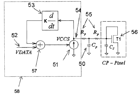
[0022] FIG. 5 is a schematic for removing the effect of parasitic capacitance
according to the present invention;
[0023] FIG. 6 shows a simple implementation of the differentiator and voltage
adder
presented in FIG. 5.
-4-
CA 02496642 2005-02-10
[0024] FIG. 7 shows the settling time of current programming for the circuit
presented
in FIG. 5, compared to the conventional driving method; and
[0025] FIG. 8 shows the settling time versus threshold voltage for the pixel
presented
in FIG. 5, compared to the conventional driving method.
DETAILED DESCRIPTION
[0026] The following description is of a preferred embodiment.
[0027] FIG. 1 shows a typical array structure of the active matrix organic
light-
emitting diode (AMOLED). The pixels 10 are arranged in rows and columns and
they
are connected to the data line 11 through a thin film transistor (TFT) 12. A
current
1 o source 13 drives the data line 11. The overlap capacitance of the TFTs 12
connected
to data line 11 and the line capacitance leads to a high parasitic
capacitance.
[0028] FIG. 2 shows the equivalent circuit for a current programmed pixel 20
during
programming cycle. CP 21 and RP 22 are the parasitic components and Cs 23 is
the
storage capacitance. If Cs 23 « CP 21 and RP 22 is small, the timing constant
of the
circuit shown in Fig. 2 is:
[0029] i a 2
* (1)
[0030] where (3 is the coefficient in current-voltage (I-V) characteristics of
the TFT
given by Ids = [i (Vgs - Vth)2. Here, Ids is the drain-source current, Vgs the
gate-
2o source voltage, and Vth the threshold voltage. The present invention is
valid for TFTs
with different values of power parameter a (assumed to be 2 for finding eqn. (
1 ))
including a-Si:H, poly-Si, organic, and nano-crystalline TFTs.
[0031 ] While CP 21 is a big capacitance (around 40pf) and (3 is small for
amorphous
silicon (a-Si) TFT 24, T is of the order of millisecond. However, the timing
budget of
programming cycle is less than 100us for large area displays. Since the
efficiency of
the OLED has been increased, the amount of current required to achieve the
-5-
CA 02496642 2005-02-10
maximum brightness is very small; therefore, T, which is also a function of
current,
increases dramatically.
[0032] FIG. 3 shows a prior art current driving method. During the programming
cycle a current sensor 30 monitors the voltage across R 31. The programming
current
is controlled by the current sensor 30. After the pixel settles, the current
flowing
through R 31 and the OLED 33 is the same as wanted current. Because of using
feedback 32, this driving method has a fast settling time. However, the
drawback of
this circuit is that it has high power consumption due to existence of a
resistor 31.
Resistor 31 should be very big resistor, in order to make the circuit able to
sense the
low current level accurately. Therefore, the power dissipated in resistor 31
is
considerable. The other drawback of this circuit is that it extremely suffers
from
mismatch. The spatial mismatch changes the value of resistor 31 and causes non-
uniformity in display. It also has an extra feedback 33 line.
[0033] FIG. 4 shows another prior art current driving method. In programming
cycle,
SCAN is high so T2 is off and T4 is on. Therefore, the current flows through
T3, the
OLED 40, and T1. A current comparator 41 defines the reference voltage 42
based on
comparison result of pixel current 43 and reference current 44. ABer pixel
settles, the
pixel current 43 is the same as reference current 44. This pixel has fast
settling time
because of using feedback. However, its drawback is high power compensation
due to
existence of two TFTs (T1 and T2) in the path of current during the driving
cycle. The
other drawback of this method is that it uses four TFTs, and extra feedback
line 43.
[0034] Fig. 5 shows a circuit in accordance with the present invention. The
circuit can
remove the effect of parasitic capacitance 50 and as a result can be used for
fast
programming of current programmed pixel 56, which is a general schematic that
represent functionality of current programmed pixels. The present invention
can be
used with any current-programmed pixel circuits. The circuit includes a
voltage
controlled current source (VCCS) 51 that is controlled by VDATA 52 and the
output
of a differentiator 53 which monitors the voltage of data line 54. The VCCS
51,
differentiator 53, and voltage adder 57 are part of the display driver 58 that
can be
3o implemented as a separate chip using CMOS technology or on-display TFT
technology.
-6-
CA 02496642 2005-02-10
[0035] If RP SS is small enough and the VCCS 51 is a linear current source,
the timing
constant for the circuit shown in FIG. S is:
[0036] z oc 2 ~C° K)
i * ~ (3)
[0037] Here 'i' is the current related to VDATA 53. K is the differentiator
coefficient
and should be selected close to CP 50 in order to achieve the best result.
However, a
reasonable difference between K and CP has no significant effect on the
settling time.
[0038] FIG. 6 shows a simple example for implementation of the differentiator
and
the voltage adder presented in FIG. S.
[0039] FIG. 7 shows the settling time for the conventional driving method and
that
1o proposed here when the programming current is 200 nA. While the settling
time for
the conventional driving method is around 800 us, it is 30 us for the circuit
in
accordance with present invention.
[0040] FIG. 8 shows the settling time versus threshold voltage of T1 for the
conventional and proposed methods. The settling time of the conventional
driving
method (dotted line) increases drastically when VT increases. However, for
method
presented here (solid line) the change is insignificant.
[0041 ] The present invention has been described with regard to one or more
embodiments. However, it will be apparent to persons skilled in the art that a
number
of variations and modifications can be made without departing from the scope
of the
invention as defined in the claims. In particular, while the active matrix
OLED
(AMOLED) architecture is considered, it should be apparent to skilled person
in the
art that the technique can also be applied to the passive matrix OLED
architecture.