Note: Descriptions are shown in the official language in which they were submitted.
CA 02496710 2005-02-21
WO 2004/027123 PCT/IB2003/004057
-1-
SINGLE CRYSTAL DIAMOND
BACKGROUND OF THE INVENTION
This invention relates to single crystal diamond.
Diamond offers a range of unique properties, including optical transmission,
thermal conductivity, stiffness, wear resistance and its electronic
properties.
Whilst many of the mechanical properties of diamond can be realised in
more than one type of diamond, other properties are very sensitive to the
type of diamond used. For example, for the best electronic properties CVD
single crystal diamond is important, often outperForming polycrystalline
CVD diamond, HPHT diamond and natural diamond.
In many applications of diamond the limited lateral dimensions of the
diamond available is a substantial limitation. Polycrystalline CVD diamond
layers have substantially removed this problem for applications where the
polycrystalline structure is suitable for the application, but in many
applications polycrystalline diamond is unsuitable.
Whilst natural and HPHT diamond may not be suitable for some
applications, they are used as substrates on which to grow CVD diamond.
Although substrates can have a variety of crystallographic orientation, the
largest and most suitable substrate orientation which can be produced for
growth of high quality CVD diamond is generally (001 ). Throughout this
specification, the Miller indices {hkl}, defining a plane based on the axes
x,y,z will be written assuming that the z direction is that normal to the
substrate surface and parallel to the growth direction. The axes x,y are
CONFIRMATION COPY
CA 02496710 2005-02-21
WO 2004/027123 PCT/IB2003/004057
-2-
then within the plane of the substrate, and are generally equivalent by
symmetry but distinct from z because of the growth direction.
Large natural single crystal diamond is extremely rare and expensive, and
large natural diamond substrate plates suitable for CVD diamond growth
have not been demonstrated because of the associated very high
economic risk in their fabrication and use. Natural diamond is often
strained and defective, particularly so in larger substrate plates, and this
causes twins and other problems in the CVD overgrowth or fracture during
synthesis. In addition, dislocations which are prevalent in the natural
diamond substrate are replicated in the CVD layer, also degrading its
electronic properties.
HPHT synthetic diamond is also limited in size, and generally is of poorer
quality in the larger stones, with inclusions being a major problem. Larger
plates fabricated from synthetic diamonds generally exhibit missing corners
so that edge facets other than {100} (such as {110}) are present, or they
are included or strained. During synthesis further facets are formed, such
as the {111} which lies between the (001) top face and the {110} side facets
(see Figure 1 of the accompanying drawings). In recent years significant
effort has been directed at synthesising HPHT diamond of high quality for
applications such as monochromators, and some progress has been
reported, but the size of HPHT plates suitable for substrates remains
limited.
{111} faces in particular are known generally to form twins during CVD
synthesis of thick layers, limiting the area of perfect single crystal growth
and often leading to degradation and even fracture during synthesis, further
exacerbated by thermal stresses resulting from the growth temperature.
Twinning on the {111 } particularly interferes with increasing the size of the
largest plate which can be fabricated with a (001 ) major face and bounded
by {100} side faces.
CA 02496710 2005-02-21
WO 2004/027123 PCT/IB2003/004057
-3-
Routinely available (001 ) substrates range up to about 7 mm square when
bounded by {100} edges, and up to about 8.5 mm across the major face
when bounded by {100} and X110} edges.
CVD homoepitaxial synthesis of diamond involves growing CVD epitaxially
on an existing diamond plate and is well described in the literature. This is
of course still limited by the availability of existing diamond plates. In
order
to achieve larger areas, the focus has been to grow laterally as well,
increasing the overall area of the overgrown plate. Such a method is
described in EP 0 879 904.
An alternative to homoepitaxial growth is heteroepitaxial growth, where a
non-diamond substrate is grown on with an epitaxial relationship. In all
reported cases however, the product of this process is quite distinct from
homoepitaxial growth, with low angle boundaries between highly oriented
but not exactly oriented domains. These boundaries severely degrade the
properties of the diamond.
Homoepitaxial diamond growth to enlarge the area of a CVD plate presents
many difficulties.
If it was possible to achieve ideal homoepitaxial growth on a diamond plate,
the growth which would be achieved is substantially that illustrated by
Figures 1 and 2 of the accompanying drawings. The growth morphology
illustrated assumes that there is no competing polycrystalline diamond
growth. However, in reality, there is generally competition from
polycrystalline growth, growing up from the surface on which the diamond
substrate plate is mounted. This is illustrated by Figure 3 of the
accompanying drawings.
Referring to Figure 3, a diamond substrate plate 10 is provided mounted on
a surface 12. Example materials for surface 12 include molybdenum,
tungsten, silicon and silicon carbide. During CVD diamond growth, single
crystal diamond growth will occur on the (001 ) face 14 and on the side
CA 02496710 2005-02-21
WO 2004/027123 PCT/IB2003/004057
-4-
surfaces, two of which 16 are shown. The side surfaces 16 are {010}
surfaces. Growth will also occur on and extend outwards from the corners
and vertices 18 of the plate. All such growth will be homoepitaxial single
crystal growth. The growth on each of the faces present on the substrate,
and on any new surfaces generated during growth, constitutes a growth
sector. For example, in Figure 3 diamond growth 24 arises from the {101}
plane and thus is the {101} growth sector.
Competing with the homoepitaxial single crystal growth will be
polycrystalline diamond growth 20 which will take place on the surface 12.
Depending on the thickness of the single crystal diamond layer produced
on the surface 14, the polycrystalline diamond growth 20 may well meet the
homoepitaxial single crystal diamond growth along line 22, as illustrated in
Figure 3.
Based on Figure 2, one might expect that the purely lateral growth on the
substrate side surfaces could be used to fabricate a larger substrate,
including the material of the original substrate. However, as is clear from
Figure 3, such a plate would actually contain competing polycrystalline
growth. A plate fabricated parallel to the original substrate, but higher up
in
the grown layer is likely to contain twinning, especially from material in the
{111} growth sector.
Under growth conditions where polycrystalline diamond does not compete
with the single crystal diamond there still remains the problem that the
quality of the lateral single crystal growth is generally poor, as a result of
the different geometry and process conditions present at the diamond
substrate edges, exacerbated by the method used to suppress
polycrystalline growth.
Defects in the substrate used for CVD diamond growth replicate into the
layer grown thereon. Clearly, since the process is homoepitaxial, regions
such as twins are continued in the new growth. In addition, structures such
as dislocations are continued, since by its very nature a line dislocation
CA 02496710 2005-02-21
WO 2004/027123 PCT/IB2003/004057
-5-
cannot simply self terminate, and the probability of two opposite
dislocations annihilating is very small. Each time a growth process is
initiated, additional dislocations are formed, primarily at heterogeneities on
the surface, which may be etch pits, dust particles, growth sector
boundaries and the like. Dislocations are thus a particular problem in
single crystal CVD diamond substrates, and in a series of growths in which
the overgrowth from one process is used as the substrate for the next, the
density of dislocations tends to increase substantially.
SUMMARY OF THE INVENTION
According to the present invention, a method of producing a plate of single
crystal diamond includes the steps of providing a diamond substrate having
a surface substantially free of surface defects, growing diamond
homoepitaxially on the surface by chemical vapour deposition (CVD) and
severing the homoepitaxial CVD grown diamond and the substrate
transverse, typically normal (that is, at or close to 90°), to the
surface of the
substrate on which diamond growth took place to produce a plate of single
crystal CVD diamond.
The homoepitaxial CVD diamond growth on the surface of the substrate
preferably takes place by the method described in WO 01/96634. Using
this method, in particular, it is possible to grow thick, high purity single
crystal diamond on a substrate. A growth thickness of the homoepitaxial
grown CVD diamond of greater than 10 mm, preferably greater than
12 mm, and more preferably greater than 15 mm, can be achieved. Thus,
it is possible, by the method of the invention, to produce single crystal CVD
diamond plates having at least one linear dimension exceeding 10 mm,
preferably exceeding 12 mm and more preferably exceeding 15 mm. By
"linear dimension" is meant any linear measurement taken between two
points on or adjacent to the major surfaces. For instance, such linear
dimension may be the length of an edge of the substrate, a measurement
CA 02496710 2005-02-21
WO 2004/027123 PCT/IB2003/004057
-6-
from one edge, or a point on the edge, to another edge, or another point on
the edge, an axis or other like measurement.
In particular, it is possible by the method of the invention to produce
rectangular (001 ) single crystal diamond plates which are bounded by {100}
side surfaces or faces which have at~least one linear dimension, such as a
linear <100> edge dimension, exceeding 10 mm, preferably exceeding
12 mm and more preferably exceeding 15 mm.
The plate of single crystal CVD diamond produced by the method may then
itself be used as a substrate in the method of the invention. Thick single
CVD crystal diamond can be grown homoepitaxially on a major surface of
the plate.
The invention provides, according to another aspect, a (001 ) single crystal
CVD diamond plate having major surfaces on opposite sides thereof
bounded by {100} side surfaces, i.e. a plate in which the major surfaces are
{001 } faces, each major surface having at least one linear dimension
exceeding 10 mm. In one form of the invention, the plate has a
rectangular, square, parallelogram or like shape, at least one of the side
surfaces of which, and preferably both side surfaces, has a dimension
exceeding 10 mm, preferably exceeding 12 mm and more preferably
exceeding 15 mm. Most preferable is that these side surfaces are {100}
surfaces or faces, such that the plate edge dimension (or dimensions)
exceeding 10 mm is in the <100> direction. Further, the method of the
invention provides for a larger plate or piece of diamond from viihich such a
plate bounded by {100} side surfaces and {001 } major surfaces can be
fabricated.
In the homoepitaxial diamond growth which occurs on the surface of the
diamond substrate, any dislocations or defects in that surface, or arising at
the interface with the substrate, or from the edges of the substrate,
generally propagate vertically in the diamond growth. Thus, if the severing
takes place substantially normal to the surface on which diamond growth
CA 02496710 2005-02-21
WO 2004/027123 PCT/IB2003/004057
-7-
took place, then the severed surface will have substantially no dislocations
within the material intersecting the surface, as they will be running
generally
parallel to the surface. Thus a reduction in the dislocation density in the
volume of the material can be achieved by repeating the method using this
new plate as the substrate, and a resulting further reduction in the density
of dislocations cutting the major surface of any plates cut normal to this
substrate. Furthermore, there are applications that benefit from plates in
which the dislocations that are present run generally parallel to the major
faces rather than generally normal to them.
Generally the highest quality CVD growth is that contained within the
vertical (001 ) growth sector. Furthermore, since the edges of the substrate
can form dislocations and these generally rise vertically upwards, then the
highest quality volume of the CVD growth is that bounded by the vertical
planes rising up from the substrate edges. The method of this invention
enables one or more new large area plates to be fabricated from entirely
within this volume, thus minimising the defects within the plate, and
maximising its crystal quality.
Combining the various features of this invention, it is possible to produce
diamond with a lower dislocation density than the starting substrate
material, with the lower limit on dislocation density set only by the number
of times the method is to be repeated. In particular, the large area plate of
the invention and any layers subsequently synthesised on it can have a
dislocation density, typically intersecting a surface normal to the growth
direction (this surface generally showing the highest dislocation density in
CVD diamond), which is less than 50/mm~, and preferably less than
20/mm2, and more preferably less than 10/mm2 and even more preferably
less than 5/mm2. The defect density is most easily characterised by optical
evaluation after using a plasma or chemical etch optimised to reveal the
defects (referred to as a revealing plasma etch), using for example a brief
plasma etch of the type described in WO 01/96634. In addition, for
applications in which the dislocation density intersecting the major face of
the plate is of primary concern, then a plate fabricated by the method of this
CA 02496710 2005-02-21
WO 2004/027123 PCT/IB2003/004057
_g_
invention can exhibit a dislocation density on its major face which is less
than 501mm~, and preferably less than 20/mm2, and more preferably less
than 10/mm2 and even more preferably less than 5/mm2.
Where the substrate is a natural or HPHT synthetic substrate, it is generally
not advantageous for the normally cut plate to include the material from the
original substrate, although this can be done. It can be advantageous to
include material from the substrate in this plate when the substrate is itself
a CVD diamond plate, which may itself have been prepared by this method.
BRIEF DESCRIPTION OF THE DRAWINGS
Figure 1 is a schematic perspective view of a diamond plate on which
ideal homoepitaxial diamond growth has taken place;
Figure 2 is a section along the line 2-2 of Figure 1;
Figure 3 is a section through a diamond plate illustrating single crystal
diamond growth and polycrystalline diamond growth;
Figure 4 is a section through a diamond plate on which homoepitaxial
diamond growth according to an embodiment of the invention
has taken place;
Figure 5 is a schematic of a diamond plate showing the angle a of the
dislocation direction relative to the major surfaces of the
diamond plate; and
Figure 6 is a schematic of a diamond plate showing the angle (3 of the
dislocation direction relative to the normal to the major
surfaces of the plate.
CA 02496710 2005-02-21
WO 2004/027123 PCT/IB2003/004057
_g_
DESCRIPTION OF AN EMBODIMENT
An embodiment of the invention will now be described with reference to the
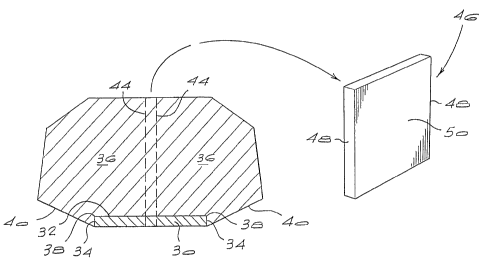
accompanying drawings. Referring to Figure 4, a diamond plate 30 is
provided. The diamond plate 30 is a plate of single crystal diamond. The
upper face 32 is the (001 ) face and the side surfaces 34 are {010} faces.
The surface 32 is substantially free of surface defects, more particularly
substantially free of crystal defects as described in WO 01/96634.
Following the method described in WO 01/96634, diamond growth 36 takes
place on the diamond substrate 30. This diamond growth occurs vertically
on the upper surface 32, outwards from the corners 38 of the substrate 30
and outwards from the side surfaces 34. This diamond growth will
generally be homoepitaxial, single crystal and of high quality, although
dislocations and twinning on the X111} may be present as described earlier.
Inevitably, some polycrystalline diamond growth will occur on the surface
on which the substrate is placed. This polycrystalline diamond growth may,
depending on the thickness of the diamond growth region 36, meet the
lower surface 40 of this region.
Once a desired thickness of diamond growth 36 has taken place, the
diamond growth region 36 and substrate 30 are severed normal (at
approximately 90°) to the surface 32, as illustrated by dotted lines
44. This
produces a plate 46 of high quality single crystal diamond. The interface
between the original substrate and the diamond growth will, for practical
purposes, be indistinguishable from the bulk of the sample. The original
substrate material may form part of plate 46 or be removed from it. More
than one plate may be produced, with each plate parallel to the next and
normal to the substrate.
Using the method of WO 01/96634, it is possible to produce a diamond
growth region 36 which exceeds 10 mm in depth. Thus, the diamond plate
CA 02496710 2005-02-21
WO 2004/027123 PCT/IB2003/004057
-10-
46 which is produced will have side surfaces 48 which exceed 10 mm in
length.
The plate 46 may be used as a substrate for the method of the invention.
Thus, if the plate 46 has side surfaces 48 greater than 10 mm in length and
diamond growth exceeding 10 mm in thickness is produced on the major
surface 50 of the plate, it is possible to produce a square, rectangular or
similar shaped plate which has all four side surfaces exceeding 10 mm in
length.
Severing in Figure 4 is shown to take place perpendicular to the surface 32.
Severing can take place at angles other than perpendicular to the surface
32, excluding plates which are parallel to the substrate. Plates produced at
angles other than normal to the substrate, where the substrate has a (001 )
major face, will have major faces other than the {100}, such as the {110},
{113}, {111} or higher order planes.
Further, it is possible to sever along planes which are at right angles to the
sever planes 44 of Figure 4, which will also form a plate with a major {100}
face, or at any other angle relative to the sever planes 44, which will form
plates with major faces of the type {hk0~. To achieve single crystal
diamond plates, some trimming of polycrystalline or defective growth at the
edges may be necessary.
Those skilled in the art will recognise that the general method need not be
restricted to substrates with a (001 ) major face, but could equally be
applied to other substrates with, for example, {110}, {113}, or even {111 }
major faces, but that in general the preferred method is to use a substrate
with a (001 ) major face, since the highest quality CVD diamond growth can
be most easily grown on this face and the disposition of facets formed on
the growing CVD on this face is generally most appropriate for the
production of large plates cut from the material grown.
CA 02496710 2005-02-21
WO 2004/027123 PCT/IB2003/004057
-11-
For this reason, the key dimension in a substrate plate with a (001) major
face is the largest rectangular plate which can be fabricated bounded only
by {100} side faces. Growth on this plate can relatively easily produce the
plate bounded by {110} side surfaces or faces which is rotated by 45°,
as
shown in Figure 1, since this makes limited or no use of {111} growth sector
material. This new plate, bounded by {110} side faces has an area which is
at least double that of the {100} bounded plate, but the original {100}
bounded plate generally remains the largest inscribed {100} bounded plate
which can be fabricated from it. For this reason, reference to the size of a
single crystal diamond plate with a (001 ) major face in this specification
often explicitly refers to the size of the largest area inscribed rectangular
plate bounded by {100} edges, if the plate does not already have {100}
edges.
Application of the method of this invention enables the manufacture of
products not previously possible. For instance, large area windows, where
for reasons of clear aperture, support, mechanical integrity, vacuum
integrity etc. an assembly of smaller windows will not suffice, are now
possible. High voltage devices, where the large area provides the
protection from arcing round the active area of the device, are also
possible. The low dislocation density material of the invention further
enables applications such as electronic devices in which dislocations act as
charge carrier traps or electrical short circuits.
The growth direction of a CVD diamond layer can generally be determined
from the dislocation structures within it. There are a range of configurations
which can be present.
1 ) The simplest case is where the dislocations all grow largely
parallel and in the direction of growth, making the growth direction
clearly evident.
2) Another common case is where the dislocations fan out slowly
about the growth direction, usually exhibiting some form of
CA 02496710 2005-02-21
WO 2004/027123 PCT/IB2003/004057
-12-
symmetry about the growth direction and at an angle typically less
than 20°, and more typically less than 15°, and even more
typically
less than 10°, and most typically less than 5° about this axis.
Again from a small area of the CVD diamond layer the growth
direction is easily determined from the dislocations.
3) On occasion, the growth face is not itself at right angles to the local
growth direction, but at some small angle away from this. Under
such circumstances the dislocations may be biased towards the
direction normal to the substrate surface of the growth zone in
which they are found. Particularly near edges, the growth direction
may vary substantially from the bulk of the layer, for example at
{101} edge bevels on a substrate with a {001} major growth face.
In both these instances, taken over the whole substrate the
general growth direction is clearly evident from the dislocation
structures, but equally evident is that the material is formed from
more than one growth sector. In applications in which the
directions of the dislocations is of importance, then it is generally
desirable to use material from only one growth sector.
For the purposes of this specification, the direction of the dislocations is
that direction which an analysis of the dislocation distribution would suggest
to be the growth direction of the layer based on the above models.
Typically and preferably, the direction of the dislocations within a
particular
growth sector will then be the mean direction of the dislocations using a
vector average, and with at least 70%, more typically 80%, and even more
typically 90% of the dislocations lying in a direction which is within
20°,
more preferably 15°, even more preferably 10° and most
preferably 5° of
the mean direction.
The direction of dislocations can be determined for example by X-ray
topography. Such methods do not necessarily resolve individual
dislocations but may resolve dislocation bundles, generally with an intensity
in part proportional to the number of dislocations in the bundle. Simple or
CA 02496710 2005-02-21
WO 2004/027123 PCT/IB2003/004057
-13-
preferably intensity weighted vector averaging is then possible from
topographs imaging cross sections in the plane of the dislocation direction,
with a topograph taken normal to that direction being distinct in having a
pattern of points rather than lines. Where the original growth direction of a
plate is known, then this is a sensible starting point from which to determine
the dislocation direction.
Having determined the dislocation direction according to the above method,
its orientation can be classified relative to the major faces of the single
crystal CVD diamond plate. Referring to Figure 5, a diamond plate 60 has
opposite major surfaces 62 and 64. The direction of the dislocations,
indicated generally by lines 66, is considered to be oriented generally
parallel to the major faces 62,64 of the diamond plate 60 if the dislocations
direction 66 makes an angle a of less than 30°, preferably less than
20°,
more preferably less than 15°, even more preferably less than
10°, and
most preferably less than 5° from a plane 68,70 of at least one of the
major
faces 62,64 of the plate 60. This orientation of dislocations is typically
achieved when the single crystal CVD diamond plate is severed
substantially perpendicular to the substrate on which growth took place, in
particular when severed from the highest quality CVD growth contained
within the vertical (001 ) growth sector.
Applications benefiting from the dislocation direction lying generally
parallel
to the major faces include optical applications where the effect on the
variation of refractive index observed across a light beam passing through
the plate is to substantially reduce the spread, compared to that when the
same dislocation distribution is substantially normal to the major surfaces.
Such applications benefit from being able to produce plates whose lateral
dimensions both exceed 2 mm, more preferably 3 mm, even more
preferably 4 mm, even more preferably 5 mm and even more preferably
7 mm, as is now made possible by the method of this invention.
Further applications benefiting from selecting the direction of the
dislocations to be generally parallel to the major faces of the plate are in
CA 02496710 2005-02-21
WO 2004/027123 PCT/IB2003/004057
-14-
applications using high voltage, where dislocations can provide a short
circuit in the direction of the applied voltage.
Another application is that of laser windows, where the effect of the beam
travelling parallel to the dislocations can enhance local electric fields and
result in failure. This can be controlled by either offsetting the dislocation
direction from the beam direction, or preferably setting the dislocation
direction parallel to the major faces of the laser window and thus at right
angles to the incident laser beam. Thus the maximum laser damage
threshold can be achieved by practicing the method of the invention.
Another way of classifying the dislocation direction is its orientation
relative
to the normal to a major face of the plate. Referring to Figure 6, a diamond
plate 80 has opposite major surfaces 82 and 84. The dislocation direction
86 is considered to be offset away from the normal 88 to at least one of the
major faces 82,84 of the plate if the angle [3 between the dislocation
direction 86, determined by the above method, and the normal 88 exceeds
20°, more preferably exceeds 30°, even more preferably exceeds
40°, and
most preferably exceeds 50°. This orientation of dislocations is
typically
achieved when the single crystal CVD diamond plate is severed at an angle
to the surface of the substrate on which growth took place. Alternatively, it
may occur where the plate is severed substantially perpendicular to the
substrate on which growth took place, but in a region where the growth face
itself is not parallel to the original substrate surface, for instance in a
{101}
growth sector of a layer grown on a (001 ) substrate.
Substantial benefit can be achieved in certain applications by ensuring the
dislocation direction is merely offset away from the normal to at least one of
the major faces of the plate. Such requirements are found in the application
of diamond to etalons.
This invention may be further understood by way of the following non-
limiting examples.
CA 02496710 2005-02-21
WO 2004/027123 PCT/IB2003/004057
-15-
Example 1
Two {001} synthetic diamond substrates were prepared for CVD diamond
growth according to the method described in WO 01/96633. A layer was
then grown onto these diamond substrates to a thickness of 6.7 mm. The
layers were characterised for their dislocation direction, and it was found
that >90% of dislocations visible~by X-ray topography were within 20°
of the
growth direction, and >80% of the dislocations were within 10° of the
growth direction.
One plate was cut out of each of these layers such that the major faces of
each plate had dimensions > 6 x 5 mm and the direction of growth was in
the plane of the major faces.
One plate was then used for a second stage of CVD diamond growth,
preparing it according to the method of WO 01/96633, thus producing a
second layer which was in excess of 4 mm thick and suitable for the
preparation of a 4 x 4 mm plate cut to include the growth direction in a
major face. This layer was then characterised for it dislocation density in
the direction of growth, by producing a small facet and using the method of
a revealing plasma etch, which found the dislocation density to be very low
and in the region of 10/mm2. This made the material particularly suited to
the application of etalons.
Example 2
In optical applications, a key parameter is the uniformity and spread in
values of properties such as birefringence and refractive index. These
properties are affected by the strain fields surrounding dislocation bundles.
Two {001} synthetic diamond substrates were prepared for CVD diamond
growth according to the method described in WO 01/96633. A layer was
grown onto this diamond to a thickness of 4 mm. The layers were
characterised for dislocation direction and it was found that the mean
CA 02496710 2005-02-21
WO 2004/027123 PCT/IB2003/004057
-16-
dislocation direction lay within 15° of the growth direction. Two
plates were
cut out of these layers such that the major faces of the plates had
dimensions > 4 x 4 mm and the direction of growth was in the plane of the
major faces.
These layers were subsequently used for substrates in a second growth
process. X-ray topography showed that the resulting growth (to a thickness
of 3.5 mm) had a very low dislocation content, and that the dislocations in
the new overgrowth were perpendicular to those in the original CVD layer
used as the substrate. Subsequent to this second growth the samples
were used in an optical application which required very low scatter and
birefringence.
Example 3
A synthetic diamond substrate was prepared for CVD diamond growth
according to the method described in WO 01196633. A layer was then
grown onto this diamond to a thickness of 7.4 mm. The synthesis
conditions were such that this layer was boron doped to a concentration, as
measured in the solid, of 7x10'6 [B] atoms/cm3. The layer was
characterised for its dislocation direction, with the mean dislocation
direction found to be within 25° of the growth direction. Two plates
were
cut out of this layer such that the major faces of the plates had dimensions
> 4 x 4 mm and the direction of growth was in the plane of the major faces.
These plates, because of the low density of dislocations intersecting the
major surfaces in combination with the boron doping, had particular use as
substrates for electronic devices such as a diamond metal semiconductor
field effect transistor (MESFET).
Example 4
A 6 x 6 mm synthetic substrate Ib was prepared using the method
described in WO 01/96633 This substrate was then grown on in stages,
CA 02496710 2005-02-21
WO 2004/027123 PCT/IB2003/004057
-17-
typically adding about 3 mm of growth in each stage. At the end of each
stage the layer was retained in the polycrystalline diamond layer that had
grown around it, this polycrystalline layer being trimmed to a disc about
25 mm diameter using laser trimming, and then this disc mounted into a
recessed tungsten or other metal disc such that the point where the single
crystal was exposed above the polycrystalline diamond layer was
approximately level (to within 0.3 mm) of the upper surface of the tungsten
disc.
Using the above technique it was possible to grow layers with a final
thickness in the range 10 - 18 mm, from which plates with {100} edges
could be vertically cut. Plates were produced with a first <100> dimension
in the plane of the plate of 10 - 16 mm, and a second orthogonal dimension
of3-8mm.
These plates were then prepared as substrates and used for a second
stage of growth, again using the above technique, to produce layers which
were 10 - 18 mm thick. From these layers it was possible to cut vertical
plates which were greater than 10 -18 mm in the <100> second dimension
within the major face and retaining the first <100> dimension in the range
- 18 mm. For example, plates were produced which were larger than 15
mm x 12 mm, the dimensions being measured in orthogonal <100>
directions.