Note: Descriptions are shown in the official language in which they were submitted.
CA 02497559 2005-03-02
WO 2004/023520 PCT/US2003/024318
-1_
Description
POWER-ON MANAGEMENT FOR VOLTAGE DOWN-CONVERTER
TECHNICAL FIELD
This invention relates to the field of power
supplies for integrated circuits, and in particular to
power-on management for on-chip voltage down-converters.
BACKGROUND ART
On-chip voltage down-converters are widely used
in integrated circuits, such as memory devices.
FIG. 1 shows a prior art voltage down-converter
in which a differential amplifier 14 drives the gate 15
of a p-channel MOS transistor 16 with its source 17
connected to the external power supply 11, Vcc EXT, and
its drain 18 connected to the internal power supply,
Vcc_INT, node 9. The first amplifier input 13 is at
internal reference voltage, Vref, by connection to
reference generator circuit 12; the control loop is
closed by connecting the second amplifier input 8 to the
Vcc INT node 9. As the current consumption of the load
circuit 19 increases, Vcc_INT will decrease; eventually
Vcc INT falls below Vref and the amplifier responds by
lowering P GATE, which increases the conductivity of the
p-channel of transistor 16, resulting in an increased
current flow to the Vcc-INT node 9. For applications
such as flash memory, in which the current consumption
has fast transients and high peak currents, the circuit
of FIG. 1 has an inadequate high frequency response, to
the extent that large drops in Vcc-INT occur at the onset
of a fast current transient; the inadequate high
frequency response is to a large extent due to the RC
constant of the Vcc-INT node 9. An improved circuit, to
overcome this deficiency, is shown in FIG. 2.
CA 02497559 2005-03-02
WO 2004/023520 PCT/US2003/024318
_2_
The prior art voltage down-converter in FIG. 2
is basically comprised of: a power device, transistor 31,
providing current at the Vcc_INT node 32; a replica
device with scaled W/L, transistor 26; and a differential
amplifier 23 with a feedback loop closed on the replica
device, for regulating G REF so as to keep Vcc REF within
a desired voltage range. The power device of the circuit
is a source follower n-channel MOS transistor 31 with a
very low threshold voltage. This transistor 31 has a
very large W/L, ensuring its operation in the weak
inversion region; this allows a small Vgs variation, even
with the wide range of current required by the load
circuit (a few ~a.A to hundreds of mA). Coupled to the
power device is a replica transistor 26 with a smaller
W/L: The transistor gates are driven by G REF, by
connection to the amplifier output 24. The first
amplifier input 22 is at Vref. The control loop is
closed on the replica device by connection of the second
amplifier input 25 to the voltage divider 28. Thus, the
amplifier 23 with its feedback loop operates to keep the
Vcc REF node 27 within an allowed voltage range. Leaving
the power device 31 and Vcc_INT node 32 out of the
feedback loop improves the stability, bandwidth and gain
control of the amplifier 23, particularly considering
that the RC constant of the Vcc_INT node 32 is not well
controlled. Sufficient bias currents must flow in the
reference circuit, Ibias ref 29, and regulated power
circuit, Ibias reg 35, in order to keep Vcc_REF and
Vcc INT within their allowed operating ranges; transistor
33, controlled by Vbias at its gate 34 can be used. to
increase Ibias reg 35, when required. Satisfactory
matching of the power device and the replica device is an
issue for this circuit design. An improved circuit, to
overcome this deficiency, is shown in FIG. 3.
CA 02497559 2005-03-02
WO 2004/023520 PCT/US2003/024318
-3-
The voltage down-converter has two modes of
operation for memory devices: a stand-by mode in which
the power consumption from the external supply must be
very low, while providing Vcc_INT with current
consumption from the device of up to lO~tA; and an active
mode in which the voltage down-converter must provide
Vcc_INT with. current consumption from the device of up to
200mA, while keeping Vcc_INT within an allowed voltage
range of 1.6V to 2V.
The prior art voltage down-converter in FIG. 3
is comprised of three sections: the replica circuit 41
that is always on and generates the control signal
OUT AMP; the stand-by section 42; and the active section
43. Each section has two n-channel transistors (47 & 48,
58 & 59, and 61 & 62) compared with the single transistor
of the design shown in FIG. 2. This configuration has
the following advantages: reduced total output
capacitance of the op-amp 44; better control of the
transition from stand-by mode to active mode; and good
de-coupling between the Vcc_INT nodes 36, 38 and the
control loop. The reference current Ibias ref 29 must be
very low to minimize current consumption during the
stand-by mode. V~hen the active mode is entered the
reference current branch is doubled (as shown for
Ibias ref 29), thus allowing the voltage down-converter
to be biased quickly; this is achieved by controlling
transistor 53 with signal Vbias. Vbias is also used to
control the current in transistors 55 and 57, allowing
faster biasing of the active and standby sections (bias
currents: Ibias act 66 and Ibias_sby 65). Since the
voltage drop at the internal supply nodes 36 and 38 for a
given device load current, Iload, depends on
log(Iload/Ibias), a minimum Ibias must be ensured for
Vcc-INT to remain within an acceptable range.
CA 02497559 2005-03-02
WO 2004/023520 PCT/US2003/024318
-4-
Consideration is now given specifically to the
power-on phase for the voltage down-converter. It is
desired to monitor both external and internal supplies,
to be able to ensure that an internal power-on starts
only when an external power-on occurs. It is also
desired to force the active mode of the voltage down-
converter at power-on. Further, it is desired to
discharge the internal supply nodes of the voltage down-
converter at the start of power-on, so as to ensure that
the power-on always starts from the same initial
condition. Furthermore, it is desired to provide a
reference voltage for operation of the voltage down-
converter, at the earliest opportunity during power-on.
It is an object of the present invention to
provide an on-chip power-on management system to control
these various power-on functions of a voltage down
converter.
SUMMARY OF THE INVENTION
The above object has been achieved by a power-
on management system for an on-chip voltage down-
converter, monitoring both external and internal voltage
supplies to independently determine when both supplies
have reached minimum levels for proper operation of on-
chip circuitry. The power-on management system supplies
output signals that: control the discharge of the
internal supply nodes at the initiation of power-on;
force the active mode of the voltage down-converter; and
deactivate a fast local voltage reference on completion
of power-on. The system comprises signal level detectors
and devices for delaying the falling edge of input
signals.
BRIEF DESCRIPTION OF THE DRAWINGS
FIG. 1 is a high level circuit diagram of a
prior art voltage down-converter.
CA 02497559 2005-03-02
WO 2004/023520 PCT/US2003/024318
-5-
FIG. 2 is a basic circuit diagram of a prior
art voltage down-converter.
FIG. 3 is a detailed circuit diagram of a prior
art voltage down-converter.
FIG. 4 is a block diagram showing a voltage
down-converter and power-on management system of the
present invention.
FIG. 5 is a basic circuit diagram of a
reference voltage generator in accord with the present
invention.
FIG. 6 is a basic circuit diagram of a current
generator in accord with the present invention.
FIG. 7 is a basic circuit diagram of an
internal Vcc node discharger of the present invention.
FIG. 8 is a signal form diagram representing an
operation of the power-on management system of the
present invention.
BEST MODE OF CARRYING OUT THE INVENTION
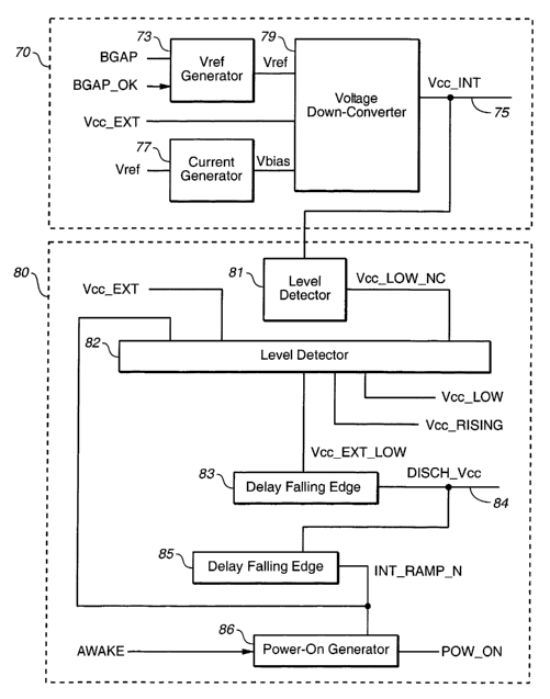
FIG. 4 shows a block diagram of the internal
voltage down-converter system 70 and power-on management
system 80 of the present invention, including input and
output signals. The voltage down converter 79 generates
a regulated internal supply, Vcc_INT, from the external
supply Vcc EXT; the output~of the voltage down-converter
79 is connected to the Vcc_INT node 75. The voltage
down-converter 79 requires a reference voltage, Vref,
which is provided lay the Vref generator 73. The voltage
down converter 79 also requires a bias current reference
voltage, Vbias, which is provided by the current
generator 77. An example of a voltage down-converter in
accord with the present invention is shown in FIG. 3.
The current generator 77 requires an input of a reference
voltage, Vref. The Vref generator 73 can produce its own
local voltage reference, or can use a temperature
CA 02497559 2005-03-02
WO 2004/023520 PCT/US2003/024318
-6-
independent bandgap voltage reference, BGAP, provided as
an input. The logic signal BGAP OK, provided as an input
to the Vref generator 73, indicates when the signal BGAP
is at its correct value, of approximately 1.23V.
The power-on management system 80, Vref
generator 73, and some components (an auxiliary current
branch) of.current generator 77 are all dedicated to the
power-on phase of operation of the voltage down-converter
79; together they can be considered as a power-on system
for the voltage down-converter.
FIG. 5 shows an example of a fast reference
voltage generator suitable for use as local Vref
generator 73 in FIG. 4. Start-up circuit 102 and
temperature compensating circuit 103 are connected to an
autobiasing current generator 104, which comprises p-
channel transistors 105 and 106 and n-channel transistors
107 and 108. The autobiasing current generator 104
controls the current in transistor 109, which is
mirrored, by the mirror circuit comprising p-channel
transistors 111 and 112, into the diode chain 113,
comprising diodes 114 and 115. A 'Dummy Vref', or local
voltage reference, is generated at node 116; a
temperature independent bandgap voltage reference, BGAP,
is connected to node 117. Switches 118 and 119 are
controlled by logic signal BGAP_OK; signal BGAP OK is
high when BGAP is at its correct value, otherwise it is
low. The switches 118 and 119 operate so that Vref at
node 121 will be provided by Dummy Vref until BGAP has
attained its correct voltage, the signal BGAP OK goes
high and changes the positions of switches 118 and 119 so
that Vref at node 121 is provided by BGAP. Further
circuits (not shown) may be incorporated into the
reference voltage generator of FIG. 5, such as disabling
and other optional circuits. An example of such a
circuit is a switch that switches the power supply,
CA 02497559 2005-03-02
WO 2004/023520 PCT/US2003/024318
_7-
Vcc EXT, for the local Vref generator 73 to ground, thus
disabling the local Vref generator, when power-on is
complete; this switch being activated by a signal POW_ON
generated by the power-on management system 80
FIG. 6 shows an example of a current generator
suitable for use as current generator 77 in FIG. 4. A
control current 142, Icontrol, is generated by n-channel
transistors 133 and 134, controlled by a constant voltage
signal, Vref, applied to their gates 132. This current
is mirrored, by the mirror circuit comprising p-channel
transistors 135 and 136, providing a reference current
143, Iref, in the reference diode 137, and providing a
reference voltage, Vbias, at node 138. When the
capacitance of the Vbias node 138 is high and the nominal
reference current 143 is low, the charging time of the
Vbias node 13 8 may be too long ( for example, tens of ~.~.s ) ;
this can be overcome (reducing the charging time to a few
~s) by increasing the control current 142 for the current
mirror during the initial charging of the Vbias node 138.
The increase in control current 142 is provided by
transistor 141; W/L of transistor 133 is much greater
than W/L of transistor 134, which allows for a much
higher control current 142 when transistor 141 is
activated. Transistor 141 is controlled by applying an
'enable auxiliary branch' signal to its gate 139; this
'enable auxiliary branch' signal can be the output signal
Vcc RISING generated by the power-on management system
80. The transistors 133 and 141 constitute the auxiliary
current branch, utilized during power-on to provide
faster charging of the Vbias node 138. Further circuits
(not shown) may be incorporated into the current
generator of FIG. 6, such as disabling, error correction
and other optional circuits.
FIG. 7 shows the internal regulated supply,
Vcc_INT, node discharger. The Vcc_INT node 151 is
CA 02497559 2005-03-02
WO 2004/023520 PCT/US2003/024318
_g_
discharged by a high voltage n-channel transistor 154,
controlled by the DISCH Vcc signal applied to its gate
153. A protection resistor 152, of typically a few ohms,
is connected between the transistor drain 155 and the
Vcc_INT node 151. The Vcc_INT node discharger functions
to discharge the internal supply nodes of the voltage
down-converter at the start of power-on, so as to ensure
that the power-on always starts from the same initial
condition.
FIG. 8 shows the form of all of the signals
identified in the power-on management system 80 in FIG.
4. Voltage is plotted against time, with the signals
spaced along the ordinate for clarity; note that all
signals start at V=0 at T0. Vcc EXT is the external
supply voltage, which in this example is 3.3V, when high.
In order to illustrate the operation of the power-on
management system, Vcc EXT is shown ramping up from its
low at OV to its high at 3.3V, ramping down to its low at
OV for a short duration and then ramping up to its high
again. Vcc_INT is the internal regulated voltage, in
this example the high is 1.8V.
Referring to FIG. 4, a first level detector 81
is connected to node 75 and senses the Vcc-INT signal
voltage level. The level detector 81 generates an
intermediate signal Vcc LOW_NC (see FIG. 8) which is tied
to Vcc_INT until a minimum voltage is reached at which
the circuitry supplied by Vcc-INT will operate properly
(in this example 1V); when Vcc-INT is at a voltage
greater than this minimum, Vcc LOW NC is low.
As seen in FIG. 4, a second level detector 82
senses the voltage levels of signals Vcc EXT, Vcc LOW NC
and INT_RAMP N. The level detector 82 generates an
intermediate signal Vcc EXT LOW (see FIG. 8) which is
tied to Vcc_EXT until a minimum voltage is reached at
which the on-chip circuitry requiring the Vcc EXT supply
CA 02497559 2005-03-02
WO 2004/023520 PCT/US2003/024318
-9-
will operate properly (in this example 2V); when Vcc_EXT
is at a voltage greater than this minimum, Vcc EXT LOW is
low. An output signal of the level detector 82 is
Vcc RISING (see FIG. 8) which is tied to INT RAMP N
except that when Vcc RISING is high, it remains high
until Vcc LOW NC goes low, then it too goes low; when
Vcc_RISING is low it indicates that both Vcc EXT and
Vcc-INT have reached voltages at which their dependent
on-chip circuitry will operate properly, even if the
power-on is still on-going. When Vcc_RISING is low it
disables the auxiliary current branch in the current
generator (see FIG. 6). A further ouput signal from
level detector 82 is Vcc LOW (see FIG. 8) which is
Vcc LOW_NC shadowed by Vcc RISING. Vcc LOW remains low
even when Vcc_INT has a glitch, as seen at T1 in FIG. 8;
Vcc LOW goes high only when Vcc EXT goes low. Output
signal Vcc LOW is used as an input for the device in
which the voltage down-converter is integrated and
indicates that a power-on is ongoing when the signal is
high.
Referring to FIG. 4, the 'delay falling edge'
device 83 (hereafter referred to as a delay device) has
intermediate signal Vcc EXT LOW as an input and generates
an output signal DISCH Vcc (see FIG. 8) which is tied to
Vcc EXT_LOW, except that it is delayed on the falling
edge, by 1~.~.s in this example; when high, DISCH Vcc
enables the discharge of the Vcc_INT nodes, which grounds
the gates of the drivers and pre-drivers and the
amplifier in the voltage down-converter. As seen in FIG.
4, a second 'delay falling edge' device 85 (hereafter
referred to as a delay device) is connected to the
DISCH_Vcc node 84. The device 85 generates an
intermediate signal INT RAMP N (see FIG. 8) which is tied
to DISCH_Vcc, except with a further delay on the falling
edge, by a fraction of a ~.~.s in this example; when
CA 02497559 2005-03-02
WO 2004/023520 PCT/US2003/024318
-10-
INT RAMP N goes low it indicates that Vcc_INT is ramping
up. Referring to FIG. 4, power-on generator 86 has a
logic signal AWAKE (see FIG. 8) as an input; this input
signal is generated by the device in which the voltage
down-converter is inserted and when high it indicates
that the internal power-on is complete. The power-on
generator 86 has intermediate signal INT RAMP N as a
further input and generates output signal POW ON (see
FIG. 8) which. is tied to INT RAMP N, except that when
POW_ON is high, it remains high until AWAKE goes high,
then it goes low. The signal POW_ON is used as follows:
when high it indicates that power-on is on-going; when
high it forces the active mode of the voltage down-
converter; and when low it turns off the local Vref
generator (see FIG. 5). The present invention is
applicable to a 3V to 1.8V voltage down-converter in a
0.18~.m technology flash memory device. It will be clear
to those skilled in the art that the present invention is
applicable to a wide range of memory devices and other
integrated circuits requiring an on-chip voltage down-
converter.