Note: Descriptions are shown in the official language in which they were submitted.
CA 02497691 2005-03-03
WO 2004/023574 PCT/US2003/027424
TITLE
METHODS FOR PRODUCING FULL-COLOR ORGANIC
ELECTROLUMINESCENT DEVICES
FIELD OF THE INVENTION
The invention relates to methods for the production of organic
electroluminescent (EL) devices that display full-color images, such as full-
color organic light emitting diodes (OLEDs).
BACKGROUND OF THE INVENTION
Organic light emitting diodes (OLEDs) are promising for display
applications due to their high power-conversion efficiency and low
processing costs. Such displays are especially promising for battery-
powered, portable electronic devices, including cell-phones, personal
digital assistants, handheld personal computers, and DVD players. These
applications call for displays with high information content, full color, and
fast video rate response time in addition to low power consumption.
Current research in the production of full-color OLEDs is directed
toward the development of cost effective, high throughput processes for
producing color pixels. For the manufacture of monochromatic displays,
spin-coating processes have been widely adopted (see, e.g., David Braun
and Alan J. Heeger, Appl. Phys. Letters 58, 1982 (1991)). However,
manufacture of full-color displays requires certain modifications to
procedures used in manufacture of monochromatic displays. For
example, to make a display with full-color images, each display pixel is
divided into three subpixels, each emitting one of the three primary display
colors, red, green, and blue. This division of full-color pixels info three
subpixels has resulted in a need to modify current processes for
depositing different organic polymeric materials onto a single substrate
during the manufacture of OLED displays.
One such process for depositing polymer layers on a substrate is
ink jetting (see, e.g., U.S. Patent Application Publication No.
200110001050). in order to form an emitting layer with a uniform
thickness, proper formulation of the ink and proper design and treatment
of the substrate is generally required. However, it has proven quite
challenging to properly design and treat substrates to form full-color
displays while maintaining suitable device performance (such as efficiency
and lifetime). For example, structures used for retaining polymer inks in
the subpixels tend to reduce the aperture ratio of a display. In addition,
methods used for surface treatment of subpixellated substrates prior to
addition of polymer inks can damage the underlying active matrix
CA 02497691 2005-03-03
WO 2004/023574 PCT/US2003/027424
substrate. Accordingly, there is a need for alternative methods for the cost
effective production of full-color EL devices that do not deleteriously effect
device performance.
SUMMARY OF THE INVENTION
The invention provides methods for the production of organic
electroluminescent (EL) devices. Substrates used in the methods of the
invention for production of EL devices do not require CF4 plasma surface
treatment prior to deposition of electroluminescent material. Thus, the
invention methods are particularly useful in the production of EL devices
where ink-jetting is used to deposit electroluminescent material. In
addition, the invention methods are useful for producing both subpixellated
and non-subpixellated devices. Moreover, the invention methods are
useful for producing EL devices which contain one type of EL material or
several types of EL material.
In another embodiment of the invention, there are provided organic
EL devices produced by providing a substrate, depositing an anode layer
onto the substrate, establishing a plurality of discreet wells on the
substrate, wherein the discreet wells are formed by circumscribing walls to
form the wells, depositing an un-patterned buffer layer onto the anode
layer in each of the wells, depositing an un-patterned EL host polymer
layer into each of said wells, depositing at least one patterned dopant
layer in at least one of said wells without prior surface treatment of the
walls of the well, and depositing a cathode layer, thereby producing an
organic electroluminescent (EL) device.
In still another embodiment of the invention, there are provided full-
color, subpixellated organic EL devices produced by providing a substrate,
depositing an anode layer onto the substrate, establishing a plurality of
discreet wells in sets of three on the substrate, wherein the discreet wells
are formed by circumscribing walls to form the wells, wherein each well
defines a subpixel and each set of three wells defines a pixel, depositing
an un-patterned buffer layer onto the anode layer in each of the wells,
depositing an un-patterned EL host polymer layer selected to produce blue
light in each of the wells, depositing a first patterned dopant layer selected
to produce red light in a first well in at least one of the set of three wells
without prior surface treatment of the walls of the well, depositing a second
patterned dopant layer selected to produce green light in a second well in
at least one of the set of three wells without prior surface treatment of the
walls of the well, and depositing a cathode layer, thereby producing an
electroluminescent device.
2
CA 02497691 2005-03-03
WO 2004/023574 PCT/US2003/027424
In yet another embodiment, there are provided electroluminescent
devices including a substrate having a plurality of discreet wells, wherein
each of the discreet wells has at least one wall surFace that is substantially
free of fluorine.
In still another embodiment, the present invention relates to
electroluminescent devices having a plurality of first and second subpixels,
containing at least one layer of electroluminescent polymer, wherein the
electroluminescent polymer layer in at least one of the first subpixels has
diffused therein a first dopant, and the electroluminescent polymer layer in
at least one of the second subpixels has diffused therein a second dopant,
and the at least one first subpixel exhibits a photoluminescence spectrum
displaying emission only from the first dopant, and the at least one second
subpixel exhibits a photoluminescence spectrum displaying emission only
from the second dopant.
BRIEF DESCRIPTION OF THE FIGURES
The invention is illustrated by way of example and not limitation in
the accompanying figures.
Figs. 1-3 illustrate exemplary alternative device structures prepared
according to the methods of the invention.
Fig. 4 illustrates intensity voltage dependence of a blue pixel (single
layer) and a red pixel (bilayer) processed by coating blue and red
polymers.
Fig. 5 illustrates EL emission spectra with single layer EL polymers.
Fig. 6 illustrates EL emission spectra produced by a device with the
structure shown in Fig. 1.
Fig. 7 illustrates EL spectra with single layer EL polymers doped
with fluorescent dopants: green dopant C545T (peak maxima 520 nm)
and red- dopant DCJTB (peak maxima 650 nm.
Fig. 8 illustrates EL spectre with single layer polymers doped with green
and red fluorescent Ir complexes.
Fig. 9 illustrates EL emission spectra with single layer EL polymers
doped with fluorescent dopants.
Fig. 10 illustrates photoluminescent spectra of CN-PPP/Dopants
under UV illumination (emission in 300 to 400 nm range is due to the UV
excitation source ).
DETAILED DESCRIPTION OF THE INVENTION
Methods are provided for the production of organic
electroluminescent devices. In one embodiment, there is provided a
3
CA 02497691 2005-03-03
WO 2004/023574 PCT/US2003/027424
method for producing an organic electroluminescent (EL) device
comprising:
a) providing a substrate,
b) depositing an anode layer onto said substrate,
c) establishing a plurality of discreet wells on said substrate,
wherein said discreet wells are formed by circumscribing walls to form said
wells,
d) depositing an un-patterned buffer layer onto said anode layer in
each of said wells,
e) depositing an un-patterned EL host polymer layer into each of
said wells,
f) depositing at least one patterned dopant layer in at least one of
said wells without prior surface treatment of said walls of said well, and
g) depositing a cathode layer,
thereby producing an organic electroluminescent (EL) device.
In another embodiment, there is provided a method for producing a
full-color, subpixellated organic electroluminescent (EL) device, the
method comprising:
a) providing a substrate,
b) depositing an anode layer onto said substrate,
c) establishing a plurality of discreet wells in sets of three on said
substrate, wherein said discreet wells are formed by circumscribing walls
to form said wells, wherein each well defines a subpixel and each set of
three wells defines a full-color pixel,
d) depositing an un-patterned buffer layer onto said anode layer in
each of said wells,
e) depositing an un-patterned EL host polymer layer selected to
produce blue light in
each of said wells,
f) depositing a first patterned dopant layer selected to produce red
light in a first well in at least one of said set of three wells without prior
surface treatment of said walls of said well,
g) depositing a second patterned dopant layer selected to produce
green light in a second well in at least one of said set of three wells
without
prior surface treatment of said walls of said well,
h) depositing a cathode layer,
thereby producing a full-color, subpixellated organic electroluminescent
device.
4
CA 02497691 2005-03-03
WO 2004/023574 PCT/US2003/027424
As used herein, the term "dopant" refers to a material suitable to
alter the light emitting properties of an un-doped host material.
As used herein, the term "un-patterned", when used in conjunction
with an organic layer used in the production of an EL device, means that
the organic layer has been deposited across the entire pixel array, as
opposed to being deposited in a specific pattern across the pixel array.
As used herein, the term "patterned", when used in conjunction with
a dopant layer used in the production of an EL device, means that the
dopant is deposited into specified wells within specified pixels across the
pixel array.
As used herein, the phrase "surface treatment" refers to a process
commonly used in the art to modify the wetting properties of the walls of
wells in subpixellated EL devices. "Surface treatment" refers to exposure
to a dry plasma, using CF4 gas after the wells are formed with walls made
of organic materials, such as photoresists or acrylic resins. As a result of
such surface treatment, the surface of the substrate and the walls of the
v wells are substantially fluorinated. As used herein, the term "fluorinated"
means that fluorine is associated with the surface of the substrate.
Fluorine may be associated with the surface in a number of ways, for
example, the fluorine may be physically adsorbed onto the surface,
chemically bonded to the surface, and the like. Indeed, those skilled in the
art recognize that a chemical analysis of a surface treated with CF4 would
show the presence of fluorine. It is commonly known that plasma CF4
treatment can damage the underlying electronic components in an active
matrix EL device, a process that limits useable process conditions for
substrates containing active matrix pixel drivers.
As used herein, the terms "comprises," "comprising," "includes,"
"including," "has," "having" or any other variation thereof, are intended to
cover a non-exclusive inclusion. For example, a process, method, article,
or apparatus that comprises a list of elements is not necessarily limited to
only those elements but may include other elements not expressly listed or
inherent to such process, method, article, or apparatus. Further, unless
expressly stated to the contrary, "or" refers to an inclusive or and not to an
exclusive or. For example, a condition A or B is satisfied by any one of the
following: A is true (or present) and B is false (or not present), A is false
(or not present) and B is true (or present), and both A and B are true (or
present).
Also, use of the "a" or "an" are employed to describe elements and
components of the invention. This is done merely for convenience and to
5
CA 02497691 2005-03-03
WO 2004/023574 PCT/US2003/027424
give a general sense of the invention. This description should be read to
include one or at least one and the singular also includes the plural unless
it is obvious that it is meant otherwise.
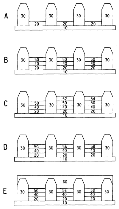
Figure 1 illustrates one embodiment of the invention for producing
full-color EL devices. The substrate is either embedded with microcircuitry
(active matrix substrate) or has no embedded microcircuitry (passive
matrix substrate). In Fig. 1A, a rigid or flexible substrate 10 is provided
with a patterned anode layer 20, and then walls 30 are provided so as to
form a plurality of wells in sets of three on the substrate. The wells may
have any convenient shape, for example, rectangular, circular (including
oval-shaped), triangular, and the like. In one embodiment, the walls form
rectangular wells. Each well contains an anode and forms a subpixel, and
each set of three wells forms a pixel. The walls may be constructed from
organic material such as epoxy resin, acrylic resin, polyimide resin, and
the like, or the walls may be constructed from inorgariic material such as
glass. Conventional photolithography techniques may be used to form the
pattern of walls and wells. Upon complete fabrication of the device, the
three subpixels will emit the three primary display colors, i.e., red, green,
and blue. Electronic devices containing subpixels improve the contrast of
a device and prevent light from leaking between pixels.
The anode surface is then cleaned to remove surface contaminants
using methods well known to those skilled in the art (for example, see US
Patent No. 5,798,170). As shown in Fig 1 B, an un-patterned buffer layer
40 is deposited onto the anode layer 20, and an un-patterned blue EL
polymer layer 50 is then coated over the entire active area (i.e., all of the
subpixels) by methods well-known to those skilled in the art e.g., spin
coating, silk-screen printing, and the like. By depositing the un-patterned
buffer layer 40 and un-patterned blue EL polymer layer 50 over the entire
active area, the need for plasma surface treatment of the walls is obviated.
In addition to providing the emission for the blue subpixels, the un-
patterned blue EL polymer layer can serve as a host to receive green and
red dopants in their respective subpixels for formation of a full-color
display.
As shown in Fig. 1 C, subpixels that emit green and red light are
next formed by ink-jetting drops of polymer solutions containing green
dopant into a first set of subpixels and ink jetting drops of polymer
solutions containing red dopant into a second set of subpixels to form the
green 52 and red 54 EL polymer layers. The polymer solutions contain
small amounts of green and red dopants in a polymer host material,
6
CA 02497691 2005-03-03
WO 2004/023574 PCT/US2003/027424
wherein the polymer host material is the same polymer used for the un-
patterned blue EL polymer layer 50. Through wetting by the green and
red polymer solutions of the unpatterned blue EL polymer layer, blend
layers 56 and 58 (Fig. 1 D) with uniform (monolayer) or gradient density
distributions of green and red dopants can be formed in the green and red
subpixels. Finally, as shown in Fig. 1 E, a cathode material 60 is deposited
over the entire surface to complete the device.
As used herein, the term "monolayer" refers to a host EL polymer
having a dopant diffused therein with a uniform density distribution,
wherein the photoluminescence spectrum of the host EL polymer
containing dopant diffused therein displays emission from the dopant only.
As used herein, the term "blend layer" refers to an EL polymer layer
that is formed when the same EL polymer is used in consecutive
deposition steps, doped or undoped, for the purpose of introducing
specific dopants into the layer that alter the characteristic luminescence of
that layer. The blend layer can have a gradient density distribution and
exhibit the characteristic photoluminescence of both the host and the
dopant, or it can have the uniform density distribution of a monolayer as
defined above.
Figure 2 illustrates another embodiment of the invention methods
for producing full-color EL devices. After formation of subpixels, anode,
and buffer layers as described above with reference to Fig. 1, patterned
green and red polymer layers 52 and 54 may be deposited into two of the
three wells in a pixel, Fig. 2A, before an un-patterned blue EL polymer 50
is deposited, Fig. 2B. In this embodiment, it is the un-patterned buffer
layer 40 coating alone that prevents wetting of the walls by the dopant
layers when they are deposited in the subpixels. As in the previous
embodiment, the host polymer for the green and red dopants is the same
polymer used for the un-patterned blue EL polymer layer 50. Through
wetting of the dopant layers 52 and 54 by the un-patterned blue EL
polymer layer 50, blend layers 56 and 58 can be formed, Fig. 2C. A
cathode layer 60 is deposited to complete the device, Fig. 2D.
Yet another embodiment of the invention methods is shown in
Figure 3. An additional un-patterned organic layer 70, which conducts
electrons and may or may not emit light, is coated before the cathode 60
and after the EL polymer layers 50, 56 and 58. This additional layer,
which lies adjacent to the cathode layer 60, facilitates injection and
transport of electrons from the cathode into the EL polymer and/or
eliminates EL quenching due to the cathode.
7
CA 02497691 2005-03-03
WO 2004/023574 PCT/US2003/027424
The manufacture of EL devices according to the invention is
advantageous for several reasons. For example, blue pixels and blue
subpixels are formed by an un-patterned deposition process (e.g., spin
coating). Thus, emission homogeneity and device performance are both
optimized. In addition, the process time for formation of each of the
polymer layers is markedly reduced by eliminating ink jet processing time
and setting time for the buffer and blue EL polymer layers. This further
reduction in process time also contributes to improved- device performance
(both efficiency and operation life).
Moreover, the gradient density profile in the green and red
subpixels is readily tuned by the wetting process when a dopant is
deposited from solution using the same host polymer as used for the un-
patterned blue EL polymer layer. This tuning provides an effective means
to optimize emission of the OLED and thus the device performance.
Indeed, since the same blue light-emitting EL materials used for blue
subpixels are used as host materials for green and red subpixels, the
intensity vs. voltage dependence of the red, green and blue subpixels
follows the same trends. This feature creates an ideal situation for color
balance and compensation in full-color displays by simplifying
corresponding driving circuits. The optional un-patterned organic layer 70
adjacent to the cathode layer 60 in Fig. 3 facilitates injection and transport
of electrons into the EL layer, thereby providing an additional means for
optimizing device performance.
The diffusion of the green and red dopants into the blue EL host
polymer can be uniform and complete. Indeed, as set forth in Examples 6,
7, 8, 10, 11 and 12 and in Figure 10, the inventive EL devices contain
green and red subpixels which exhibit photoluminescence spectra
displaying emission from the green and red dopants only. Thus, in one
embodiment of the invention, there are provided EL devices comprising a
substrate, an anode layer, an electroluminescent polymer layer selected to
produce blue light, and a cathode layer, wherein in at least one first
subpixel the electroluminescent polymer layer has diffused therein a first
dopant selected to produce red light and in at least one second subpixel
the electroluminescent polymer layer has diffused therein a second dopant
selected to produce green light, wherein the at least one first subpixel
exhibits a photoluminescence spectrum displaying emission only from the
first dopant, and the at least one second subpixel exhibits a
photoluminescence spectrum displaying emission only from the second
dopant. Those skilled in the art recognize that the methods of this
8
CA 02497691 2005-03-03
WO 2004/023574 PCT/US2003/027424
invention are not limited to producing red, green, and blue subpixellated
full-color displays, but can be used to form any number of subpixels with
any combination of characteristic emissions, based on the properties of
the electroluminescent materials used.
Furthermore, when EL devices are produced according to the
methods of the invention, there is no need for surface treatment of the
substrate prior to deposition of either the un-patterned blue EL polymer or
the red and green dopant materials. Those skilled in the art recognize that
plasma surface treatment of wells prior to deposition of polymer layers can
damage the underlying substrate and especially damage the transistors
embedded in the substrate of an active matrix device. Indeed, the
surfaces of the walls of the wells employed in the invention EL devices are
substantially free of fluorine. As used herein, the phrase "substantially
free of fluorine" means that the surfaces contain an amount of fluorine
which is normally present, based on the composition of the materials, and
is to be distinguished from an amount of fluorine that would be present on
the surface after surface treatment with CF4.
Substrates 10 contemplated for use in the practice of the invention
can be flexible or rigid, organic or inorganic. Generally, glass or organic
films in either rigid or flexible form are used as a support. The anode layer
20 is an electrode that is more efficient for injecting holes compared to the
cathode layer. The anode can include materials containing a metal, mixed
metal, alloy, metal oxide or mixed oxide. Suitable materials include, but
are not limited to, the mixed oxides of the Group 2 elements (i.e., Be, Mg,
Ca, Sr, Ba, Ra), the Group 11 elements, the elements of Groups 4, 5, and
6, and the Group 8-10 transition elements. Group numbers corresponding
to columns within the periodic table of the elements use the "New
Notation" convention as seen in the CRC Handbook of Chemistry and
Physics, 81St Edition (2000).
If the anode layer is to be light transmitting in the visible spectral
range, mixed oxides of Groups 12, 13 and 14 elements, such as indium-
tin-oxide, may be used. As used herein, the phrase "mixed oxide" refers
to oxides having two or more different cations selected from the Group 2
elements or the Groups 12, 13, or 14 elements. Some non-limiting,
specific examples of materials for the anode layer include indium-tin-oxide
("ITO"), aluminum-tin-oxide, gold, silver, copper, and nickel. The anode
may also comprise an organic material, such as a conducting polyaniline
(G. Gustafsson, Y. Cao, G. M. Treacy, F. Klavetter, N. Colaneri, and A.J.
Heeger, Nature 357, 477 (1992)), PEDOT-PSSA (Y. Cao, G. Yu, C.
9
CA 02497691 2005-03-03
WO 2004/023574 PCT/US2003/027424
Zhang, R. Menon and A.J. Heeger, Synth. Metals, 87, 171 (1997)) and
polypyrrole-4-dodecylbenzenesulfonic acid (DBSA) (J. Gao, A.J. Heeger,
J.Y. Lee and C.Y. Kim, Synth. Metals 82, 221 (1996)).
The anode layer may be formed by a chemical or physical vapor
deposition process or by a spin-cast process. Chemical vapor deposition
may be performed as a plasma-enhanced chemical vapor deposition
("PECVD") or metal organic chemical vapor deposition ("MOCVD").
Physical vapor deposition can include all forms of sputtering, including ion
beam sputtering, as well as e-beam evaporation and resistance
evaporation. Specific forms of physical vapor deposition include rf
magnetron sputtering and inductively-coupled plasma physical vapor
deposition ("IMP-PVD"). These deposition techniques are well known
within the semiconductor fabrication arts.
Usually, the anode layer is patterned using a lithographic operation.
The pattern may vary as desired. The layers can be formed in a pattern
by, for example, positioning a patterned mask or resist on the first flexible
composite barrier structure prior to applying the first electrical contact
layer
material. Alternatively, the layers can be applied as an overall layer (also
called blanket deposit) and subsequently patterned using, for example, a
patterned resist layer and wet chemical or dry etching techniques. Other
processes for patterning that are well known in the art can also be used.
When the electronic devices form a passive matrix array, the anode layer
typically is formed into substantially parallel strips having lengths that
extend in substantially the same direction. In an active matrix array, the
anode layer is patterned to form a discrete electrode for each electronic
device, or subpixel.
The buffer layer 40 functions to facilitate injection of holes into the
EL polymer layer and to smoothen the anode surface to prevent shorts in
the device. Buffer layers are typically polymeric materials, such as
polyaniline (PANI) or polyethylenedioxythiophene (PEDOT), which are
often doped with protonic acids, or can be organic charge transfer
compounds, and the like, such as the tetrathiafulvalene-
tetracyanoquinodimethane system (TTF-TCNQ). Protonic acids
contemplated for use in the practice of the invention include, for example,
poly(styrenesulfonic acid), poly(2-acrylamido-2-methyl-1-propanesulfonic
acid), and the like. The buffer layer is usually cast onto substrates using a
variety of techniques well known to those skilled in the art. Typical casting
techniques include, for example, solution casting, drop casting, curtain
casting, spin-coating, screen printing, inkjet printing, and the like.
CA 02497691 2005-03-03
WO 2004/023574 PCT/US2003/027424
Alternatively, the buffer layer can be patterned using a number of such
processes, such as ink-jet printing.
The electroluminescent (EL) layer 50 may typically be a conjugated
polymer such as poly(paraphenylenevinylene) (PPV), PPV copolymers,
polyfluorenes, polyphenylenes, polyacetylenes, polyalkylthiophenes, and
the like. The particular material chosen may depend on the specific
application, voltage potentials used during operation, or other factors. The
EL layer can also be made with oligomers or dendrimers
Dopants contemplated for use in the practice of the invention are
typically organometallic materials. Exemplary metals contemplated for
use include lanthanide metals (e.g., Eu, Tb), Group 7 metals (e.g., Re),
Group 8 metals (e.g., Ru, Os), Group 9 metals (e.g., Rh, Ir), Group 10
metals. (e.g., Pd, Pt), Group 11 metals (e.g., Au), Group 12 metals (e.g.,
Zn), Group 13 metals (e.g., AI), and the like. In one embodiment, the
organometallic materials may be cyclometallated complexes of Ir or Pt,
with ligands such as phenylpyridines. Typical cyclometallated complex
dopants contemplated for use in the practice of the invention are disclosed
in published PCT application WO 02/2714, the entire contents of which are
incorporated herein by reference. In another embodiment, the
organometallic materials may be functionalized polymers comprising
functional groups coordinated to at least one metal. The metals may be
those discussed above. Exemplary functional groups contemplated for
use include carboxylic acids, carboxylic acid salts, sulfonic acid groups,
sulfonic acid salts, groups having an OH moiety, amines, imines, diimines,
N-oxides, phosphines, phosphine oxides, ~i-dicarbonyl groups, and the
like. Typical polymeric organometallic dopants contemplated for use in the
practice of the invention are disclosed in Published PCT Application No.
WO 02/31896, the entire contents of which are incorporated herein by
reference.
Dopants contemplated for use in the practice of the invention can
also be an organic dye molecule such as 4-dicyanmethylene-2-methyl-6-
(p-dimethyaminostyryl) 4H-pyran (DCM), coumarin and the like. Dopants
contemplated for use in the practice of the invention can also be a red or
green EL polymer in conjugated or non-conjugated form.
When used for the production of full-color EL devices, a first dopant
is selected to emit red light (with emission profile dominating in 600-700
nm range) and a second dopant is selected to emit green light (with
emission profile dominating in 500-600 nm range). After deposition of
each of the dopants, each pixel column contains three subpixels wherein
11
CA 02497691 2005-03-03
WO 2004/023574 PCT/US2003/027424
one subpixel emits red light, one subpixel emits green light, and one
subpixel emits blue light (with emission profile dominating in 400-500 nm
range).
As shown in Fig. 3, an optional un-patterned layer 70 may be
deposited prior to deposition of the cathode layer. This optional layer can
function both to facilitate electron injection/transport, and also serve as a
confinement layer to prevent quenching reactions at layer interfaces.
More specifically, this layer may promote electron mobility and reduce the
likelihood of a quenching reaction if the EL polymer layer and the cathode
layer would otherwise be in direct contact. Examples of materials for this
optional un-patterned layer include metal-chelated oxinoid compounds
(e.g., AIq3 or the like); phenanthroline-based compounds (e.g.,
2,9-dimethyl-4,7-diphenyl-1,10-phenanthroline ("DDPA"), 4,7-diphenyl-
1,10-phenanthroline ("DPA"), or the like); azole compounds (e.g., 2-(4-
biphenylyl)-5-(4-t-butylphenyl)-1,3,4-oxadiazole ("PBD" or the like), 3-(4-
biphenylyl)-4-phenyl-5-(4-t-butylphenyl)-1,2,4-triazole ("TAZ" or the like);
other similar compounds; or any one or more combinations thereof.
Alternatively, the optional unpatterned layer may be inorganic and
comprise BaO, LiF, Li20, or the like. This optional unpatterned layer can
also be an oligomer, dendrimer or conjugated polymer. Examples of
conjugated polymers for this layer are provided in Published PCT
Application No. WO 01/77203.
The cathode layer 60 is an electrode that is particularly efficient for
injecting electrons or negative charge carriers. The cathode layer can be
any metal or nonmetal having a lower work function than the first electrical
contact layer (in this case, the anode layer). As used herein, the term
"lower work function" is intended to mean a material having a work
function no greater than about 4.4 eV. As used herein, "higher work
function" is intended to mean a material having a work function of at least
approximately 4.4 eV.
Materials for the cathode layer can be selected from alkali metals of
Group 1 (e.g., Li, Na, K, Rb, Cs,), the Group 2 metals (e.g., Mg, Ca, Ba, or
the like), the Group 12 metals, the lanthanides (e.g., Ce, Sm, Eu, or the
like), and the actinides (e.g., Th, U, or the like). In one embodiment, the
cathode comprises materials such as aluminum, indium, yttrium, barium,
lithium, cerium, cesium, europium, rubidium, magnesium, samarium, and
combinations thereof. The cathode can also be a metal alloy, for example,
BaAI, LiAI, CaAI, Caln, and the like, or can be in a multiple layer form with
each layer containing a different metal or metal alloy composition. In this
12
CA 02497691 2005-03-03
WO 2004/023574 PCT/US2003/027424
case, only the layer adjacent to the organic emission layer or optional
electron transport layer requires a lower work function. The thickness of
the first layer is typically in the range of 1-300 nm.
The cathode layer is usually formed by a chemical or physical vapor
deposition process. The cathode layer can be patterned, as discussed
above in reference to the anode layer, or un-patterned. If the device lies
within a passive matrix array, the cathode layer may be patterned into
substantially parallel strips, where the lengths of the cathode layer strips
extend in substantially the same direction and substantially perpendicular
to the lengths of the anode layer strips. The pixels are formed- at the cross
points (where an anode layer strip intersects a cathode layer strip when
the array is seen from a plan or top view). If the device lies within an
active matrix array, the cathode can be un-patterned, or monolithic, with
the pixels and subpixels defined by the patterning of the anode layer.
The different layers may have any suitable thickness. The
inorganic anode layer is usually no greater than approximately 500 nm, for
example, approximately 10-200 nm; the buffer layer is usually no greater
than approximately 500 nm, for example, approximately 20-200 nm; the
EL layer is usually no greater than approximately 200 nm, for example,
approximately 10-80 nm; the optional un-patterned layer is usually no
greater than approximately 100 nm, for example, approximately 20-80 nm;
and the cathode layer is usually no greater than approximately 1000 nm,
for example, approximately 50-500 nm. If the anode layer or the cathode
layer needs to transmit at least some light, the thickness of such layer may
not exceed approximately 100 nm.
In organic light emitting diodes (OLEDs), electrons and holes,
injected from the cathode and anode layers, respectively, into the EL
layer, form negative and positively charged polarons in the polymer.
These polarons migrate under the influence of the applied electric field,
forming a polaron exciton with an oppositely charged species and
subsequently undergoing radiative recombination. A sufficient potential
difference between the anode and cathode, usually less than
approximately 15 volts, and in many instances no greater than
approximately 5 volts, may be applied to the device. The actual potential
difference may depend on the use of the device in a larger electronic
component. In many embodiments, the anode layer is biased to a positive
voltage and the cathode layer is at substantially ground potential or zero
volts during the operation of the electronic device. A battery or other
13
CA 02497691 2005-03-03
WO 2004/023574 PCT/US2003/027424
power sources) may be electrically connected to the electronic device as
part of a circuit.
The invention will now be described in greater detail by reference to
the following non-limiting examples.
EXAMPLES
The following specific examples are meant to illustrate and not limit
the scope of the invention.
EXAMPLE 1
OLEDs according to the invention were fabricated in the following
order:
ITO/buffer polymer/EL polymer/cathode
The substrates were 30 x 30 mm ITO coated glass. The buffer layer was
a PEDOT material (BAYTRON-P, Bayer AG, Germany). The EL polymers
were polyfluorene derivative blue and green materials (Blue-1, Blue-2,
Blue-3, Green-1 ), or bis-cyclometallated iridium complexes (Ir-R1 ) for red
emission. The EL polymer layer was spin-coated to a thickness of 77-100
nm. Toluene was used for the solution casting of the blue and green EL
materials and dichloromethane was used for the solution casting of red Ir
complex EL materials. The cathode used was 3.5 nm Ba with 500 nm AI.
Green and blue reference devices with a single coating of EL
polymer were also fabricated for comparison. The reference devices
were made by spin-coating the EL polymer in a 1-1.5 % solution of
polymer in toluene followed by immediate cathode deposition.
For the "bilayer" devices, a thin layer (30-40 nm) of the blue EL
polymer was spin-coated, and the layer was annealed for 10 minutes at
60°C followed by spinning of the second layer (40-50 nm). For the red
device, the second layer was applied as a toluene solution of a polymer
containing up to 5 % (50 mg in 1 ml of solution) of an Ir complex red
emitter in the same blue polymer host as the blue layer.
Device performance is summarized in Table 1. The data
demonstrate that one can use a double layer configuration without
sacrificing efficiency or operation voltage. In fact, the structures depicted
in Figs. 1-3 provide a unified relationship between emission intensity and
operation voltage. Fig. 4 illustrates the intensity-voltage dependence of a
blue pixel (single layer) and a red pixel (bilayer) processed by coating blue
and red polymers. This unique intensity-voltage dependence allows a
simple circuit for color balance and generalized gamma-curve correction.
14
CA 02497691 2005-03-03
WO 2004/023574 PCT/US2003/027424
TABLE
1
Device
performance
for
(RGB)
single
and
bilayer
devices
at 200
cd/m2
Device Structure Voltage EL efficiency EL Color
m (V) (cd/A)
lA Blue-1 7.0 1.5 blue
1B Blue-1 6.4 1.8 blue
1C Blue-1/Blue-2 5.9 1.6 blue
1D Blue-2 4.7 3.0 blue
lE Blue-2 5.2 3.7 blue
1F Green-1 4.9 4.4 green
1G Blue-1/Green-1 4.5 4.7 green
IH Blue-I/Green-1 4.5 4.4 green
lI Blue-2/Green-1 4.1 3.0 green
1J Blue-2/Ir-Rl 5.2 1.2 red
1K Blue-2/Ir-Rl 5.7 0.7 red
IL Blue-2/Ir-R1 5.5 0.8 red
1M Blue-I/Ir-Rl 6.3 0.8 red
1N Blue-2/Blue-3, Ir-R1 6.8 1.5 red
1O Blue-3, Ir-Rl 10.0 1.3 red
In addition, EL spectra for single layer and bilayer devices are
shown in Figs. 5 and 6, respectively. Red, green and blue emissions,
which form the fundamental color subpixels in full-color displays, were
demonstrated.
EXAMPLE 2
In this Example, devices were fabricated as in Example 1, but with
a spin-coated cyano-polyp-phenylene) (CN-PPP) blue layer (~70 nm),
The green devices were produced by vapor deposition of a green dopant
molecule (Coumarin 545T, Eastman Kodak Co., Rochester, New York)
over the blue EL polymer layer, One of the devices was treated under
toluene solvent vapor to iet the green dopant diffuse into the blue EL
polymer host. Another device was heated to allow the dopant to diffuse
into the host. The cathode was prepared as in Example 1. Red devices
were prepared in the same manner as the green devices, using a red
dopant (DCJTB, Eastman Kodak Co.). The results are summarized in
Table 2.
CA 02497691 2005-03-03
WO 2004/023574 PCT/US2003/027424
TABLE
2
Device
performance
for
(RGB)
single
layer
devices
Device Structure Voltage EL intensity EL Color
m (V) (cd/mz)
2A CN-PPPBa/Al 9 12 blue
2B CN-PPP:C545T/LiF/Al 16 2 green
2C CN-PPP:DCJTB/LiF/Al 18 2 red
EL emission spectra produced by single layer EL polymers doped
with fluorescent dopants are shown in Fig. 7. This example demonstrated
that green and red pixels can be prepared by depositing dopant molecules
on top of a blue EL polymer layer. Diffusing a layer into a single organic
layer with a desired density profile can be achieved by post heating or
solvent vapor treatment.
EXAMPLE 3
Example 1 was repeated using a soluble poly(aryl-
oxadiazole) conjugated polymer to form a continuous, un-patterned
electron transport layer before the cathode was deposited. Its thickness
was 20-30 nm. The cathode materials used in this experiment were
calcium and aluminum.
Red, green, and blue color emissions were observed in the
corresponding devices. The emission spectra were the same as those
shown in Fig. 6. The operating voltages and EL efficiencies from Ca
devices can be better than those in the Ba devices used in Example 1.
This example demonstrated that high efficiency RGB OLEDs can
be fabricated with cathode materials with higher work functions than those
most commonly used. Air stable cathodes (such as AI) can be used for
full-color PLED displays.
EXAMPLE 4
In this example, devices were fabricated as in example 1, but with a
CN-PPP spin-coated blue layer (~70 nm). Green emitters were obtained
by spin-coating a green Ir complex dopant (Ir-G1 ) (see, Y. Wang et al. ,
Appl. Phys. Lett. 79, 449 (2001 )) over the blue polymer layer. Red
devices were also made according to the same procedure but the green
dopant was replaced with a red Ir complex dopant (Ir-R2) (similar to that in
Example 1 ). The emission spectra of these devices are shown in Fig. 8.
The corresponding EL efficiencies are shown in Table 3.
16
CA 02497691 2005-03-03
WO 2004/023574 PCT/US2003/027424
TABLE
3
Device
performance
for
(RGB)
single
layer
devices
Device Structure Voltage EL intensity EL Color
m (V) (cd/m2)
4A CN-PPPBa/Al 9 12 blue
4B CN-PPP:Ir-GlBalA1 9 10 green
4C CN-PPP:Ir-R2Ba/Al 15 6 red
This example demonstrates that the green and red emitters can be
made by coating a phosphorescent dopant molecule onto a blue EL
polymer layer using a solution process (such as drop coating, jetting, etc.).
Single green and red EL blend layers with desired density profiles can be
achieved by proper selection of solvent and process conditions.
EXAMPLE 5
Column and row addressable, passive matrix OLED displays
were fabricated following the procedure described in Example 2. After
spin-coating the buffer layer and a polyspiro blue EL polymer layer (Blue-
4), green and red molecular dopants were deposited into defined areas by
means of a pair of shadow masks. In this experiment, Alq was used as an
optional electron transport layer in the green and red zones. A
Ca(5nm)/AI(200nm) double layer cathode was used in this ExampIe.~Fig. 9
shows the EL spectra of a full-color, passive matrix display made by this
procedure. The testing results at 100 cd/m~ are listed in Table 4. This
example demonstrated that red and green pixels and full-color passive
matrix displays can be made with blue polymer/dopant in a mufti-layer
structure.
2c
TABLE
4
Pixel
performance
for
(RGB)
mufti-layer
device
at
100
cd/mz
Pixel Structure Voltage EL efficiency EL Color
ID (V) (cd/A)
5A Blue-4BalA1 7.0 1.5 blue
5B Blue-4/Alq:C545/AlqBalA14.9 4.4 green
5C Blue-4/AIq:DCJTB/AIqBalAI5.2 1.2 red
EXAMPLE 6
In this Example, Example 5 was repeated with the following
modifications. After spin-coating a buffer layer and a blue EL polymer
layer, green and red molecular dopants were vapor deposited into defined
areas by means of a pair of shadow masks. The dopants were then
diffused into the underlying blue EL polymer layer to form single green and
red monolayers, by exposing the panel to organic solvent vapor.
17
CA 02497691 2005-03-03
WO 2004/023574 PCT/US2003/027424
Exemplary solvent vapors that can be used for this purpose include
xylene, toluene, chlorobenzene, etc., with a toluene vaporization
temperature of 70° C. Fig. 10 shows PL emission spectra of the green
and red subpixels. The spectral structure of the excitation source
(saturated in 300-400 nm range) is also included. The corresponding
photoluminescence images of the panel taken under UV illumination
distinctly show the formation of red and green colors without residual blue
emission spectra in the defined red and green zones, confirming the
formation of both a red and a green polymer monolayers.
EXAMPLE 7
In this Example, a device was fabricated as in Example 5, however,
the dopant was diffused into the host layer by thermal treatment rather
than diffusion from a wetting process. After spin-coating a buffer layer and
a blue EL polymer layer, green and red molecular dopants were deposited
into defined areas by means of a pair of shadow masks. The panel was
then heated under vacuum, or under a N2 or Ar atmosphere at 200 °C for
10 minutes. The formation of a red and green polymer blend monolayers
was confirmed by PL imaging and PL spectra as in the previous example.
EXAMPLE 8
Example 5 was repeated using an external biasing field for a
diifiusion process. After spin-coating the buffer layer and the blue EL
polymer layer, green and red molecular dopants were deposited into
defined areas by means of a pair of shadow masks, followed by cathode
deposition. The diffusion of red and green dopants into the blue EL
polymer layer was observed when the device was biased to a field of 1 x
105 V/cm. The formation of red and green polymer monolayers was
confirmed by photoluminescence (PL) imaging and PL spectra after the
biasing process.
Examples 6, 7 and 8 demonstrated that full-color displays can be
made with dopant (fluorescent or phosphorescent) dispersed red and
green molecules using various difFusion processes (thermal, solvent vapor
and bias field) disclosed in this invention.
EXAMPLE 9
Experiments in Examples 5-8 were repeated with active matrix
substrates. Similar color perFormance was observed. These results
demonstrated that the dopant coating and dispersion processes disclosed
in this invention can be used for different types of substrates.
18
CA 02497691 2005-03-03
WO 2004/023574 PCT/US2003/027424
EXAMPLE 10
Blue, green and red color pixels were fabricated as in Example 1.
The substrate size was 4"x 4". The active area was 3.2" x 2.4" with 4"
diagonal direction. The color pixel size was 100 pixels-per-inch (ppi)
(equivalent to 254 ~.m). Blue subpixels were formed by spin-coating a
blue EL polymer over the entire substrate. Red and green subpixels were
formed by applying the corresponding red and green polymer solution
drops into defined areas with a commercial ink-fetter made by MicroFab
Technologies, Inc., (Piano, Texas). Jetting green and red polymer
ZO solutions (1:1 ratio of p-xylene:anisole) into the corresponding subpixels
produced green and red polymer blend monolayers automatically. This
was confirmed by photoluminescence image and PL spectra.
This example demonstrated that high resolution, full-color display
pixels can be fabricated by coating an un-patterned blue layer and ink-
jetting green and red polymer solutions into the corresponding zones,
similar to the process described in Fig. 1.
EXAMPLE 11
Example 10 was repeated. The blue EL layer was formed by spin
coating a blue EL polymer over the entire panel. Red and green subpixels
were formed by applying the corresponding EL dopant molecule solutions
into defined areas. Ink-jetting green and red molecular dopant solutions
into the corresponding zones forms green and red polymer monolayers
automatically, as confirmed by photoluminescence imaging and PL
spectra. This example demonstrated that high resolution, full-color display
pixels can be fabricated by means of coating un-patterned blue layer and
ink jetting green and red EL dopant solutions into the corresponding
zones.
EXAMPLE 12
Example 10 was repeated. The blue EL layer was formed by spin-
coating a blue EL polymer over the entire panel. Red and green subpixels
were formed by depositing drops of polymer/molecular blend solutions
made with a blue host polymer and green or red dopants (either
fluorescent or phosphorescent molecules or polymers). Ink jetting green
and red polymer/molecular blend solutions into their corresponding zones
formed green and red polymer/molecular blend monolayers automatically,
as confirmed by photoluminescence imaging and PL spectra in green and
red zones. This example demonstrated that high resolution, full-color
display pixels can be fabricated by means of coating an un-patterned blue
19
CA 02497691 2005-03-03
WO 2004/023574 PCT/US2003/027424
layer and drop-coating green and red poiymer/molecule blend solutions
into their corresponding zones.
EXAMPLE 13
Example 10 was repeated with an active matrix substrate with pixel
driver circuit embedded into each pixel. The physical dimensions of the
color pixels and the corresponding subpixels were identical to that used in
Example 10. A video rate, full-color, 320x240 QVGA (Quarter Video
Graphics Array) active matrix PLED display was fabricated. This example
demonstrated that high resolution, video rate (60 frames per second), full-
IO color active matrix PLED displays can be fabricated using the method
disclosed in this invention.
While the invention has been described in detail with reference to
certain preferred embodiments thereof, it will be understood that
modifications and variations are within the spirit and scope of that which is
described and claimed.