Note: Descriptions are shown in the official language in which they were submitted.
CA 02497786 2005-03-03
WO 2004/025749 PCT/US2003/024555
DIFFUSION BARRIER COATINGS HAVING GRADED COMPOSITIONS AND
DEVICES INCORPORATING THE SAME
BACKGROUND OF THE INVENTION
The present invention relates generally to composite films having improved
resistance
to diffusion of chemical species and to devices incorporating such composite
films. In
particular, the present invention relates to light-emitting devices having at
least an
organic electroluminescent material that incorporate such composite films and
have
improved stability in the environment.
Electroluminescent ("EL") devices, which may be classified as either organic
or
inorganic, are well known in graphic display and imaging art. EL devices have
been
produced in different shapes for many applications. Inorganic EL devices,
however,
typically suffer from a required high activation voltage and low brightness.
On the
other hand, organic EL devices ("OELDs"), which have been developed more
recently, offer the benefits of lower activation voltage and higher brightness
in
addition to simple manufacture, and, thus, the promise of more widespread
applications.
An OELD is typically a thin film structure formed on a substrate such as glass
or
transparent plastic. A light-emitting layer of an organic EL material and
optional
adjacent semiconductor layers are sandwiched between a cathode and an anode.
The
semiconductor layers may be either hole (positive charge)-injecting or
electron
(negative charge)-injecting layers and also comprise organic materials. The
material
for the light-emitting layer may be selected from many organic EL materials.
The
light emitting organic layer may itself consist of multiple sublayers, each
comprising a
different organic EL material. State-of-the-art organic EL materials can emit
electromagnetic ("EM") radiation having narrow ranges of wavelengths in the
visible
spectrum. Unless specifically stated, the terms "EM radiation" and "light" are
used
interchangeably in this disclosure to mean generally radiation having
wavelengths in
the range from ultraviolet ("UV") to mid-infrared ("mid-IR") or, in other
words,
wavelengths in the range from about 300 nm to about 10 micrometer. To achieve
white light, prior-art devices incorporate closely arranged OELDs emitting
blue,
green, and red light. These colors are mixed to produce white light.
Conventional OELDs are built on glass substrates because of a combination of
transparency and low permeability of glass to oxygen and water vapor. A high
-1-
CA 02497786 2005-03-03
WO 2004/025749 PCT/US2003/024555
permeability of these and other reactive species can lead to corrosion or
other
degradation of the devices. However, glass substrates are not suitable for
certain
applications in which flexibility is desired. In addition, manufacturing
processes
involving large glass substrates are inherently slow and, therefore, result in
high
manufacturing cost. Flexible plastic substrates have been used to build OLEDs.
However, these substrates are not impervious to oxygen and water vapor, and,
thus,
are not suitable per se for the manufacture of long-lasting OELDs. In order to
improve the resistance of these substrates to oxygen and water vapor,
alternating
layers of polymeric and ceramic materials have been applied to a surface of a
substrate. It has been suggested that in such multilayer barriers, a polymeric
layer acts
to mask any defects in an adjacent ceramic layer to reduce the diffusion rates
of
oxygen and/or water vapor through the channels made possible by the defects in
the
ceramic layer. However, an interface between a polymeric layer and a ceramic
layer
is generally weak due to the incompatibility of the adjacent materials, and
the layers,
thus, are prone to be delaminated.
Therefore, there is a continued need to have robust films that have reduced
diffusion
rates of environmentally reactive materials. It is also very desirable to
provide such
films to produce flexible OELDs that are robust against degradation due to
environmental elements.
SUMMARY OF THE INVENTION
The present invention provides a substrate having at least a coating disposed
on a
surface thereof, which coating is capable of reducing diffusion rates of
chemical
species therethrough. The coating comprises a material the composition of
which
varies across a thickness thereof. Such a coating will be termed
interchangeably
hereinafter a "diffusion-barrier coating having graded composition," "graded-
composition diffusion-barrier coating," "graded-composition barrier coating,"
"diffusion-barrier coating," or simply "graded-composition coating."
In one aspect of the present invention, the substrate comprises a polymeric
material.
In another aspect of the present invention, a region between the substrate and
the
coating is diffuse such that there is a gradual change from the composition of
the bulk
substrate to the composition of the portion of the coating adjacent to the
substrate. In
this embodiment, a material of the coating adjacent to the substrate
penetrates into the
substrate.
-2-
CA 02497786 2005-03-03
WO 2004/025749 PCT/US2003/024555
In still another aspect of the present invention, at least a substrate having
a diffusion-
barrier coating having graded composition is included in an assembly
comprising a
device sensitive to chemical species to protect such an assembly from attack
by these
chemical species.
In still another aspect of the present invention, such a device is an OELD,
which
comprises a pair of electrodes and an organic light-emitting layer sandwiched
therebetween.
In yet another aspect of the present invention, an OELD is sandwiched between
two
films, each having a diffusion-barrier coating having graded composition.
The present invention also provides a method for making a substrate coated
with a
diffusion barrier coating having a graded composition. The method comprises
the
steps of. (a) providing a substrate having a substrate surface; (b) depositing
a coating
material having a first composition on the substrate surface; and (c) changing
a
composition of the coating material substantially continuously such that the
composition of the coating varies from the first composition to a second
composition
across a thickness of the coating.
In another aspect of the present invention, a method for making an assembly
comprising a device that is sensitive to chemical species comprises the steps
of. (a)
providing at least a substrate coated with a diffusion barrier coating having
a graded
composition; and (b) disposing the device on the substrate.
In another aspect of the present invention, such a device is an OELD, and the
method
comprises the steps of. (a) providing at least a substrate coated with a
diffusion barrier
coating having a graded composition; (b) forming a first electrode on the
substrate; (c)
forming an organic light-emitting layer on the first electrode; and (d)
forming a
second electrode on the organic light-emitting layer.
In still another aspect of the present invention, an OLED comprising a pair of
electrodes and an organic light-emitting layer disposed between the pair of
electrodes
and a substrate coated with a diffusion barrier coating having a graded
composition
are laminated together to form a light source.
Other features and advantages of the present invention will be apparent from a
perusal
of the following detailed description of the invention and the accompanying
drawings
in which the same numerals refer to like elements.
-3-
CA 02497786 2005-03-03
WO 2004/025749 PCT/US2003/024555
BRIEF DESCRIPTION OF THE DRAWINGS
Figure 1 is a schematic diagram of a deposition apparatus using the expanding
thermal-plasma chemical-vapor deposition.
Figure 2 is a schematic diagram of the apparatus of Figure 1 used in a
continuous
deposition.
Figure 3 is a schematic diagram of a deposition apparatus using the radio-
frequency
plasma-enhanced chemical-vapor deposition.
Figure 4 shows the elemental composition at various depths of a graded-
composition
barrier coating of the present invention.
Figure 5 compares the oxygen transmission rates through an uncoated substrate
and
one that is coated with a graded-composition barrier coating.
Figure 6 compares the water transmission rates through an uncoated substrate
and one
that is coated with a graded-composition barrier coating.
Figure 7 shows the relative light transmission through a substrate having a
graded-
composition barrier coating compared to that through an uncoated substrate.
Figure 8 shows schematically a device used with a substrate having a graded-
composition barrier coating.
Figure 9 shows schematically a construction of an OELD.
Figure 10 shows another embodiment of an OELD including a hole injection
enhancement layer.
Figure 11 shows another embodiment' of an OELD including a hole injection
enhancement layer and a hole transport layer.
Figure 12 shows another embodiment of an OELD including an electron injecting
and
transporting layer.
Figure 13 shows an OELD sealed between a substrate having a graded-composition
barrier coating and a reflective layer.
-4-
CA 02497786 2005-03-03
WO 2004/025749 PCT/US2003/024555
Figures 14 shows an OELD sealed between two substrates, each having a graded-
composition barrier coating.
Figure 15 shows a sealed OELD having a light conversion layer.
DETAILED DESCRIPTION OF THE INVENTION
The present invention, in one aspect, provides a substrate having at least a
coating
disposed on a surface thereof, which coating is capable of reducing diffusion
rates of
chemical species through the substrate. The coating comprises a material, the
composition of which varies across a thickness thereof. Such a coated
substrate finds
uses in providing protection to many devices or components; e.g., electronic
devices,
that are susceptible to reactive chemical species normally encountered in the
environment. In another example, such a substrate or film having a diffusion-
barrier
coating having graded composition can advantageously be used in packaging of
materials, such as foodstuff, that are easily spoiled by chemical or
biological agents
normally existing in the environment.
Organic light-emitting material and/or cathode materials in OELDs are
susceptible to
attack by reactive species existing in the environment, such as oxygen, water
vapor,
hydrogen sulfide, SOX, NOX, solvents, etc. Films having a graded-composition
diffusion-barrier coating are particularly useful to extend the life of these
devices and
render them more commercially viable. A barrier coating of the present
invention
may be made by depositing reaction or recombination products of reacting
species
onto a substrate or film. Varying the relative supply rates or changing the
identities of
the reacting species results in a coating that has a graded composition across
its
thickness. Thus, a coating of the present invention does not have distinct
interfaces at
which the composition of the coating changes abruptly. Such abrupt changes in
composition tend to introduce weak spots in the coating structure where
delamination
can easily occurs. Substrate materials that benefit from having a graded-
composition
diffusion-barrier coating are organic polymeric materials; such as
polyethyleneterephthalate ("PET"); polyacrylates; polycarbonate; silicone;
epoxy
resins; silicone-functionalized epoxy resins; polyester such as Mylar (made by
E.I. du
Pont de Nemours & Co.); polyimide such as Kapton H or Kapton E (made by du
Pont), Apical AV (made by Kanegafugi Chemical Industry Company), Upilex (made
by UBE Industries, Ltd.); polyethersulfones ("PES," made by Sumitomo);
polyetherimide such as Ultem (made by General Electric Company); and
polyethylenenaphthalene ("PEN").
-5-
CA 02497786 2005-03-03
WO 2004/025749 PCT/US2003/024555
Suitable coating compositions of regions across the thickness are organic,
inorganic,
or ceramic materials. These materials are typically reaction or recombination
products of reacting plasma species and are deposited onto the substrate
surface.
Organic coating materials typically comprise carbon, hydrogen, oxygen, and
optionally other minor elements, such as sulfur, nitrogen, silicon, etc.,
depending on
the types of reactants. Suitable reactants that result in organic compositions
in the
coating are straight or branched alkanes, alkenes, alkynes, alcohols,
aldehydes, ethers,
alkylene oxides, aromatics, etc., having up to 15 carbon atoms. Inorganic and
ceramic
coating materials typically comprise oxide; nitride; carbide; boride; or
combinations
thereof of elements of Groups IIA, IIIA, IVA, VA, VIA, VIIA, IB, and IIB;
metals of
Groups IIIB, IVB, and VB; and rare-earth metals. For example, silicon carbide
can be
deposited onto a substrate by recombination of plasmas generated from silane
(SiH4)
and an organic material, such as methane or xylene. Silicon oxycarbide can be
deposited from plasmas generated from silane, methane, and oxygen or silane
and
propylene oxide. Silicon oxycarbide also can be deposited from plasmas
generated
from organosilicone precursors, such as tetraethoxysilane (TEOS),
hexamethyldisiloxane (HMDSO), hexamethyldisilazane (HMDSN), or
octamethylcyclotetrasiloxane (D4). Silicon nitride can be deposited from
plasmas
generated from silane and ammonia. Aluminum oxycarbonitride can be deposited
from a plasma generated from a mixture of aluminum tartrate and ammonia. Other
combinations of reactants may be chosen to obtain a desired coating
composition.
The choice of the particular reactants is within the skills of the artisans. A
graded
composition of the coating is obtained by changing the compositions of the
reactants
fed into the reactor chamber during the deposition of reaction products to
form the
coating.
Coating thickness is typically in the range from about 10 urn to about 10000
nm,
preferably from about 10 urn to about 1000 nm, and more preferably from about
10
nm to about 200 nm. It may be desired to choose a coating thickness that does
not
impede the transmission of light through the substrate, such as a reduction in
light
transmission being less than about 20 percent, preferably less than about 10
percent,
and more preferably less than about 5 percent. The coating may be formed by
one of
many deposition techniques, such as plasma-enhanced chemical-vapor deposition
("PECVD"), radio-frequency plasma-enhanced chemical-vapor deposition
("RFPECVD"), expanding thermal-plasma chemical-vapor deposition ("ETPCVD"),
sputtering including reactive sputtering, electron-cyclotron-resonance plasma-
-6-
CA 02497786 2005-03-03
WO 2004/025749 PCT/US2003/024555
enhanced chemical-vapor deposition (ECRPECVD"), inductively coupled plasma-
enhanced chemical-vapor deposition ("ICPECVD"), or combinations thereof.
Figure 1 schematically illustrates a reactor 10 and associated equipment for
the
ETPCVD technique. At least one cathode 20, typically made of tungsten, is
disposed
in a cathode housing 30. Anode plate 40 is disposed at one end of cathode
housing
30. Optionally, at least a cathode housing is electrically floating. A voltage
applied
between cathode 20 and anode 40 generates an arc for plasma generation. A
carrier
gas, such as argon, is fed through line 50 to the arc. A plasma is generated
and exits a
nozzle or orifice 70 at the center of anode 40. A first reactant gas can be
fed through
line 60 into the carrier gas line at a point between cathode 20 and anode 40.
A second
reactant gas is fed through supply line 80 to a point downstream from orifice
70.
Supply line 80 may also terminate with a perforated ring disposed within
expanding
plasma beam 84 for better mixing. Other reactant supply lines can be provided
for
different reactant species. Radicals are generated from reactant gases,
combined,
carried to substrate 90, and deposited thereon, which substrate is supported
on
substrate holder 100. Substrate holder 100 is disposed opposite and at a
distance from
nozzle 70 and is movable relative to nozzle 70 by substrate-holder shaft 110.
Reactor
is kept under vacuum via vacuum connection 112. For example, when the coating
on the substrate is desired to comprise silicon nitride, the first reactant
gas can be
ammonia, and the second reactant gas can be silane. The relative supply rates
of first
and second reactant gases are varied during deposition to vary the composition
of the
deposited material as the coating is built up. Although Figure 1 schematically
shows
a substrate as a single piece 90, a coating may be deposited on a continuous
substrate
in similar equipment. For example, Figure 2 shows a supply roll 120 of a thin
polymeric substrate 115, which supply roll 120 is disposed on one side of
substrate
holder 100, and a take-up roll 122 disposed on the other side of substrate
holder 100.
As roll 120 continuously unwinds and roll 122 continuously winds, uncoated
substrate
film 115 continuously receives the coating material as it passes over
substrate holder
100. In another embodiment of the invention, substrate film 115 passes through
an
area opposite to many overlapping plasma beams, each being generated with
different
or varying compositions to receive a coating, the composition of which varies
continuously though its thickness.
In the ETPCVD technique, the plasma is generated at a high pressure compared
to the
regular PECVD technique. The plasma in arc channel 65 has a velocity on the
order
-7-
CA 02497786 2005-03-03
WO 2004/025749 PCT/US2003/024555
of sound velocity. The plasma expands supersonically into reactor chamber 10
via
nozzle 70 and moves subsonically toward substrate 90.
Figure 3 schematically shows reactor 200 and associated equipment for the
RFPECVD technique. Radio frequency ("RF") power is applied to cathode 210,
which is disposed in reactor 200, by RF generator and amplifier 204 and
matching
network 208, which comprises a plurality of electrical and/or electronic
components
for generating appropriate impedance or other electrical characteristics of
the overall
system to maximize power transfer from RF generator and amplifier 204.
Substrate
90 is disposed on substrate holder 100 opposite to cathode 210 to receive
plasma
deposition. Substrate holder may be grounded or electrically coupled to
another RF
generator and matching network, if a different potential is desired. A
reactant gas or a
mixture of gases is fed into a gas distributor 212 through a gas supply 214.
Gas
distributor 212 may have any shape that promotes a substantially uniform
distribution
of gases. For example, it may be a ring having perforations directed toward
substrate
holder 100. Alternatively, cathode 210 may itself be hollow and porous and
receives
reactant gases. A plasma is generated and maintained by the RF field and flows
toward substrate 90. Precursor species in the plasma are combined and
deposited on
substrate 90. The composition of the coating can be varied while it is built
up by
varying the composition of the reactant gas mixture fed into distributor 212.
A
continuous substrate such as a polymeric film may be coated with a graded-
composition coating by providing an unwinding supply roll and a take-up roll,
as
described above. The substrate likewise can travel opposite to a plurality of
deposition stations, which supply varying gas compositions, to produce a
continuous
film having a graded-composition coating.
ECRPECVD is another suitable deposition technique. This method operates at low
pressure, typically less than about 0.5 mm Hg, and typically without
electrodes. A
discharge is generated by microwave. A magnetic field is used to create the
resonance
condition of the electron gas, which results in a very high degree of
ionization due to
electron acceleration at a distance away from the substrate. The low pressure
preserves a high number density of free radicals until the plasma reaches the
substrate
and prevents normally undesirable severe bombardment thereof.
ICPECVD is another electrodeless deposition technique that can create high-
density
plasma at low pressure. A plasma is generated by an electromagnetic field
generated
by a concentric induction coil disposed outside one end of the deposition
chamber.
-8-
CA 02497786 2005-03-03
WO 2004/025749 PCT/US2003/024555
The substrate is disposed in the deposition chamber at the opposite end.
Deposition
can typically be carried out at pressure much less than 0.5 mm Hg.
In another embodiment of the present invention, the energy of the ions in a
plasma
may be controlled such that they penetrate into a surface layer of the
substrate to
create a diffuse transition region between the composition of the bulk
substrate and
the composition of the coating. Such a transition prevents an abrupt change in
the
composition and mitigates any chance for delamination of the coating.
A graded-composition coating having a thickness of about 500 nm was formed on
a
polycarbonate substrate having a dimension of about 10 cm x 10 cm and a
thickness
of about 0.2 mm using the RFPECVD technique and tested for water vapor and
oxygen transmission. Silane (maximum flow rate of about 500 standard
cm3/minute),
ammonia (maximum flow rate of about 60 standard cm/minute), and propylene
oxide
(maximum flow rate of about 500 standard cm3/minute) were used to produce the
graded coating comprising silicon, carbon, oxygen, and nitrogen. The rates of
the
reactant gases were varied during deposition so that the composition of the
coating
varied continuously across its thickness. The power fed to the RF electrode
was about
100 W when plasma was generated from propylene oxide, and about 200 W when a
mixture of silane and ammonia was fed into the reactor. The vacuum level in
the
reactor was about 0.2 mm Hg and the average temperature was about 55 C.
Figure 4
shows the elemental composition of the coating, as measured by dynamic XPS, as
a
function of sputtering time to remove portions of the thickness of the coating
during
the dynamic XPS testing, which is directly related to the depth of the
coating.
Oxygen and water vapor transmission test results are shown in Figures 5 and 6.
The
oxygen transmission rate through the coated plastic substrate was reduced by
over
three orders of magnitude compared to the uncoated substrate, and the water
vapor
transmission rate by over two orders of magnitude. Light transmission at
various
wavelengths of the visible spectrum through the coated substrate is shown in
Figure 7.
The reduction in light transmission in the blue to red region (about 430 Mn to
about
700 nm) was generally less than 7 percent.
A plastic substrate coated with a graded-composition coating, which is formed
by any
method disclosed above can be advantageously used to produce flexible light
sources
based on organic light-emitting materials. Other electronic devices that can
benefit
from the protection afforded by a graded-composition coating are, for example,
displays including liquid crystal displays, photovoltaic devices, flexible
integrated
circuits, or components of medical diagnostic systems. The term "flexible"
means
-9-
CA 02497786 2005-03-03
WO 2004/025749 PCT/US2003/024555
being capable of being bent into a shape having a radius of curvature of less
than
about 100 cm. The term "substantially transparent" means allowing a total
transmission of at least about 50 percent, preferably at least about 80
percent, and
more preferably at least 90 percent, of light in the visible range (i.e.,
having
wavelength in the range from about 400 nm to about 700 nm). It should be
understood that the composition of a graded-composition barrier coating does
not
necessarily vary monotonically from one surface to the other surface thereof.
A
monotonically varying composition is only one case of graded-composition for
the
barrier of the present invention.
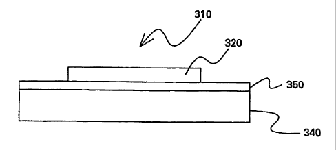
Figure 8 is a schematic diagram of an embodiment of the present invention. It
should
be understood that the figures accompanying this disclosure are not drawn to
scale.
OELD or a light-emitting device 310 comprises an organic EL member 320
disposed
on a substantially transparent substrate 340 having a graded-composition
barrier
coating 350, as described above. The graded-composition barrier coating 350
may be
disposed or otherwise formed on either or both of the surfaces of the
substrate 340
adjacent to the organic EL member 320. Preferably, the graded-composition
barrier
coating 350 is disposed or formed on the surface of the substrate 340 adjacent
to the
organic EL member 320 or it may completely cover the substrate 340. Although
Figure 8 shows schematically a distinct interface between substrate 340 and
coating
350, such a coating may be formed such that there is no sharp interface
therebetween,
as described above.
Substrate 340 may be a single piece or a structure comprising a plurality of
adjacent
pieces of different materials and has an index of refraction (or refractive
index) in the
range from about 1.05 to about 2.5, preferably from about 1.1 to about 1.6.
Preferably, substrate 340 is made of a substantially transparent polymeric
material.
Examples of suitable polymeric materials are polyethylenterephathalate
("PET"),
polyacrylates, polycarbonate, silicone, epoxy resins, silicone-functionalized
epoxy
resins, polyester, polyimide, polyetherimide, PES, PEN, polynorbonenes, or
poly(cyclic olefins).
Light-emitting member 320 comprises at least one layer 330 of at least one
organic
EL material sandwiched between two electrodes 322 and 338, as shown in Figure
9.
As will be disclosed below, the light-emitting member may comprise one or more
additional layers between an electrode and the layer 330 of organic EL
material.
When a voltage is supplied by a voltage source 326 and applied across
electrodes 322
and 338, light emits from the organic EL material. In a preferred embodiment,
-10-
CA 02497786 2005-03-03
WO 2004/025749 PCT/US2003/024555
electrode 322 is a cathode injecting negative charge carriers (electrons) into
organic
EL layer 330 and is made of a material having a low work function; e.g., less
than
about 4 eV. Low-work function materials suitable for use as a cathode are K,
Li, Na,
Mg, La, Ce, Ca, Sr, Ba, Al, Ag, In, Sn, Zn, Zr, Sm, Eu, alloys thereof, or
mixtures
thereof. Preferred materials for the manufacture of cathode layer 322 are Ag-
Mg, Al-
Li, In-Mg, and Al-Ca alloys. Layered non-alloy structures are also possible,
such as a
thin layer of a metal such as Ca (thickness from about 1 to about 10 nm) or a
non-
metal such as LiF, covered by a thicker layer of some other metal, such as
aluminum
or silver. In this embodiment, electrode 338 is an anode injecting positive
charge
carriers (or holes) into organic layer 330 and is made of a material having a
high work
function; e.g., greater than about 4.5 eV, preferably from about 5 eV to about
5.5 eV.
Indium tin oxide ("ITO") is typically used for this purpose. ITO is
substantially
transparent to light transmission and allows at least 80% light transmitted
therethrough. Therefore, light emitted from organic electroluminescent layer
330 can
easily escape through the ITO anode layer without being seriously attenuated.
Other
materials suitable for use as the anode layer are tin oxide, indium oxide,
zinc oxide,
indium zinc oxide, cadmium tin oxide, and mixtures thereof. In addition,
materials
used for the anode may be doped with aluminum or fluorine to improve charge
injection property. Electrode layers 322 and 338 may be deposited on the
underlying
element by physical vapor deposition, chemical vapor deposition, ion beam-
assisted
deposition, or sputtering. A thin, substantially transparent layer of a metal
is also
suitable.
Although the preferred order of the cathode and anode layers 322 and 338 is
disclosed
above, the electrode layers may be reversed. Electrode layers 322 and 338 may
serve
as the anode and cathode, respectively. Typically, the thickness of the
cathode layer
in this case is about 200 nm.
Organic EL layer 330 serves as the transport medium for both holes and
electrons. In
this layer these excited species combine and drop to a lower energy level,
concurrently emitting EM radiation in the visible range. Organic EL materials
are
chosen to electroluminesce in the desired wavelength range. The thickness of
the
organic EL layer 330 is preferably kept in the range of about 100 to about 300
Mn.
The organic EL material may be a polymer, a copolymer, a mixture of polymers,
or
lower molecular-weight organic molecules having unsaturated bonds. Such
materials
possess a delocalized t-electron system, which gives the polymer chains or
organic
molecules the ability to support positive and negative charge carriers with
high
-11-
CA 02497786 2005-03-03
WO 2004/025749 PCT/US2003/024555
mobility. Suitable EL polymers are poly(N-vinylcarbazole) ("PVK", emitting
violet-
to-blue light in the wavelengths of about 380-500 nm); poly(alkylfluorene)
such as
poly(9,9-dihexylfluorene) (410-550 nm), poly(dioctylfluorene) (wavelength at
peak
EL emission of 436 nm), or poly {9,9-bis(3,6-dioxaheptyl)-fluorene-2,7-diyl}
(400-
550 nm); poly(praraphenylene) derivatives such as poly(2-decyloxy-1,4-
phenylene)
(400-550 mu). Mixtures of these polymers or copolymers based on one or more of
these polymers and others may be used to tune the color of emitted light.
Another class of suitable EL polymers is the polysilanes. Polysilanes are
linear
silicon-backbone polymers substituted with a variety of alkyl and/or aryl side
groups.
They are quasi one-dimensional materials with delocalized a-conjugated
electrons
along polymer backbone chains. Examples of polysilanes are poly(di-n-
butylsilane),
poly(di-n-pentylsilane), poly(di-n-hexylsilane), poly(methylphenylsilane), and
poly{bis(p-butylphenyl)silane} which are disclosed in H. Suzuki et al., "Near-
Ultraviolet Electroluminescence From Polysilanes," 331 Thin Solid Films 64-70
(1998). These polysilanes emit light having wavelengths in the range from
about 320
urn to about 420 nm.
Organic materials having molecular weight less than about 5000 that are made
of a
large number of aromatic units are also applicable. An example of such
materials is
1,3,5-tris{n-(4-diphenylaminophenyl) phenylamino}benzene, which emits light in
the
wavelength range of 380-500 nm. The organic EL layer also may be prepared from
lower molecular weight organic molecules, such as phenylanthracene,
tetraarylethene,
coumarin, rubrene, tetraphenylbutadiene, anthracene, perylene, coronene, or
their
derivatives. These materials generally emit light having maximum wavelength of
about 520 nm. Still other suitable materials are the low molecular-weight
metal
organic complexes such as aluminum-, gallium-, and indium-acetylacetonate,
which
emit light in the wavelength range of 415-457 nm, aluminum-
(picolymethylketone)-
bis{2,6-di(t-butyl)phenoxide} or scandium-(4-methoxy-picolylmethylketone)-
bis(acetylacetonate), which emits in the range of 420-433 nm. For white light
application, the preferred organic EL materials are those emit light in the
blue-green
wavelengths.
More than one organic EL layer may be formed successively one on top of
another,
each layer comprising a different organic EL material that emits in a
different
wavelength range. Such a construction can facilitate a tuning of the color of
the light
emitted from the overall light-emitting device 310.
-12-
CA 02497786 2011-08-03
125397 (RD)
Furthermore, one or more additional layers may be included in light-emitting
member
320 to increase the efficiency of the overall device 310. For example, these
additional
layers can serve to improve the injection (electron or hole injection
enhancement
layers) or transport (electron or hole transport layers) of charges into the
organic EL
layer. The thickness of each of these layers is kept to below 500 nm,
preferably
below 100 nm. Materials for these additional layers are typically low-to-
intermediate
molecular weight (less than about 2000) organic molecules. They may be applied
during the manufacture of the device 310 by conventional methods such as spray
coating, dip coating, or physical or chemical vapor deposition. In one
embodiment of
the present invention, as shown in Figure 10, a hole injection enhancement
layer 336
is formed between the anode layer 338 and the organic EL layer 330 to provide
a
higher injected current at a given forward bias and/or a higher maximum
current
before the failure of the device. Thus, the hole injection enhancement layer
facilitates
the injection of holes from the anode. Suitable materials for the hole
injection
enhancement layer are arylene-based compounds disclosed in US Patent 5,998,
803;
such as 3,4,9,10-perylenetetra-carboxylic dianhydride or bis(1,2,5-
thiadiazolo)-p-
quinobis(1, 3-dithiole).
In another embodiment of the present invention, as shown in Figure 11, light-
emitting
member 320 further includes a hole transport layer 334 which is disposed
between the
hole injection enhancement layer 336 and the organic EL layer 330. The hole
transport layer 334 has the functions of transporting holes and blocking the
transportation of electrons so that holes and electrons are optimally combined
in the
organic EL layer 330. Materials suitable for the hole transport layer are
triaryldiamine, tetraphenyldiamine, aromatic tertiary amines, hydrazone
derivatives,
carbazole derivatives, triazole derivatives, imidazole derivatives, oxadiazole
derivatives having an amino group, and polythiophenes as disclosed in US
Patent
6,023,371.
In still another embodiment of the present invention, as shown schematically
in Figure
12, light-emitting member 320 includes an additional layer 324 which is
disposed
between the cathode layer 322 and the organic EL layer 330. Layer 324 has the
combined function of injecting and transporting electrons to the organic EL
layer 330.
Materials suitable for the electron injecting and transporting layer are metal
organic
complexes such as tris(8-quinolinolato) aluminum, oxadiazole derivatives,
perylene
derivatives, pyridine derivatives, pyrimidine derivatives, quinoline
derivatives,
quinoxaline derivatives, diphenylquinone derivatives, and nitro-substituted
fluorene
-13-
CA 02497786 2008-07-24
125397 (RD)
derivatives, as disclosed in US Patent 6,023,371.
A reflective metal layer 360 may be disposed on organic EL member 320 to
reflect
any radiation emitted away from the substantially transparent substrate 340
and direct
such radiation toward the substrate 340 such that the total amount of
radiation emitted
in this direction is increased. Reflective metal layer 360 also serves an
additional
function of preventing diffusion of reactive environmental elements, such as
oxygen
and water vapor, into the organic EL element 320. Such a diffusion otherwise
can
degrade the long-term performance of the OELD. Suitable metals for the
reflective
layer 360 are silver, aluminum, and alloys thereof. It may be advantageous to
provide
a thickness that is sufficient to substantially prevent the diffusion of
oxygen and water
vapor, as long as the thickness does not substantially reduce the flexibility
of the
entire device. In one embodiment of the present invention, one or more
additional
layers of at least a different material, such as a different metal or metal
compound,
may be formed on the reflective layer to further reduce the rate of diffusion
of oxygen
and water vapor into the organic EL member. In this case, the material for
such
additional layer or layers need not be a reflective material. Compounds, such
as metal
oxides, nitrides, carbides, oxynitrides, or oxycarbides, may be useful for
this purpose.
In another embodiment of the present invention, as shown in Figure 13, a
bonding
layer 358 of a substantially transparent organic polymeric material may be
disposed
on the organic EL member 320 before the reflective metal layer 360 is
deposited
thereon. Examples of materials suitable for forming the organic polymeric
layer are
polyacrylates such as polymers or copolymers of acrylic acid, methacrylic
acid, esters
of these acids, or acylonitrile; poly(vinyl fluoride); poly(vinylidene
chloride);
poly(vinyl alcohol); copolymer of vinyl alcohol and glyoxal (also known as
ethanedial
or oxaaldebyde); polyethyleneterephthalate, parylene (thermoplastic polymer
based
on p-xylene), and polymers derived from cycloolefms and their derivatives
(such as
poly(arylcyclobutene) disclosed in U.S. Patents 4,540,763 and 5,185,391).
Preferably, the bonding layer material is an electrically insulating and
substantially
transparent polymeric material. A suitable material is polyacrylates.
In another embodiment of the present invention, as shown in Figure 14, a
second
polymeric substrate 370 having a graded-composition bather coating 372 is
disposed
on organic EL member 320 opposite to substrate 340 to form a complete seal
around
organic EL member 320. Graded-composition barrier coating 372 may be disposed
-14-
CA 02497786 2005-03-03
WO 2004/025749 PCT/US2003/024555
on either side of substrate 370. It may be preferred to dispose graded-
composition
barrier coating 372 adjacent to organic EL member 320. Second polymeric
substrate
370 having graded-composition barrier coating 372 may also be disposed on
reflective
metal layer 360 to provide even more protection to organic EL member 320.
Alternatively, graded-composition barrier 372 may be deposited directly on
organic
EL member 320 instead of being disposed on a second polymeric substrate (such
as
370). In this case, the second substrate (such as 370) may be eliminated.
Alternatively, second substrate 370 having graded-composition barrier coating
372
can be disposed between organic EL member 320 and reflector layer 360. This
configuration may be desirable when it can offer some manufacturing or cost
advantage, especially when the transparency of coated substrate 370 is also
substantial.
In another embodiment of the present invention, the light-emitting device 310
further
comprises a light-scattering material disposed in the path of light emitted
from the
light-emitting device 310 to provide more uniform light therefrom. For
example,
Figure 15 illustrates an embodiment comprising a layer 390 of scattering
material
disposed on the substrate 340. The light-scattering material is provided by
choosing
particles that range in size from about 10 nm to about 100 micrometers. A
preferred
embodiment includes particles about 4 micrometers in size. For example, for a
device
emitting white light, the particle size is preferably on the order of 50-65
nm. Particles
of the light-scattering material may be advantageously dispersed in a
substantially
transparent polymeric film-forming material such as those disclosed above, and
the
mixture is formed into a film which may be disposed on the substrate 340.
Suitable
light-scattering materials are solids having refractive index higher than that
of the film
forming material. Since typical film forming materials have refractive indices
between about 1.3 to about 1.6, the particulate scattering material should
have a
refractive index higher than about 1.6 and should be optically transparent
over the
target wavelength range. In addition, it is preferable that the light
scattering material
be non-toxic and substantially resistant to degradation upon exposure to
normal
ambient environments. For a device designed to provide visible illumination
(wavelength in the range of about 400-700 nm), examples of suitable light-
scattering
materials are rutile (Ti0), hafiiia (Hf02), zirconia(Zr02), zircon
(Zr02=Si02),
gadolinium gallium garnet (Gd3Ga5O12), barium sulfate, yttria (Y2O3), yttrium
aluminum garnet ("YAG", Y3A15O12), calcite (CaCO3), sapphire (A1203), diamond,
magnesium oxide, germanium oxide. It is necessary to prepare these compounds
with
-15-
CA 02497786 2005-03-03
WO 2004/025749 PCT/US2003/024555
a high degree of optical purity; i.e. impurities that absorb light in the
wavelength
range of interest must be rigorously minimized. It is not necessary that the
compound
be stoichiometrically pure, phase pure, and may contain appropriate atomic
substitutions; e.g., Gd may be substituted for up to 60% of the yttrium in
YAG.
Particles composed of high- refractive index glasses, such as may be obtained
from
Schott Glass Technologies or Coming, Inc. may also be used, provided that they
are
impervious to darkening from exposure to light emitted by the OELD and its
phosphors. Scattering of light may also be achieved with a plastic or glass
film
having a roughened or textured surface (a "diffuser film"), the roughened
features of
which are typically on the order of a fraction of the wavelength of the
scattered light.
In one embodiment of the present invention, one surface of the substrate can
be
textured or roughened to promote light scattering.
According another aspect of the present invention, the light-scattering
particles in
layer 390 can comprise a photoluminescent ("PL") material (or also herein
called a
"phosphor"), which is capable of absorbing a portion of the EM radiation
emitted by
the organic EL member having a first wavelength range and emitting EM
radiation
having a second wavelength range. Thus, inclusion of such a PL material can
provide
a tuning of color of light emitted from the OELD. The particle size and the
interaction between the surface of the particle and the polymeric medium
determine
how well particles are dispersed in polymeric materials to form the film or
layer 390.
Many micrometer-sized particles of oxide materials, such as zirconia, yttrium
and
rare-earth garnets, and halophosphates, disperse well in standard silicone
polymers,
such as poly(dimethylsiloxanes) by simple stirring. If necessary, other
dispersant
materials (such as a surfactant or a polymeric material like poly(vinyl
alcohol)) may
be added such as are used to suspend many standard phosphors in solution. The
phosphor particles may be prepared from larger pieces of phosphor material by
any
grinding or pulverization method, such as ball milling using zirconia-
toughened balls
or jet milling. They also may be prepared by crystal growth from solution, and
their
size may be controlled by terminating the crystal growth at an appropriate
time. The
preferred phosphor materials efficiently absorb EM radiation emitted by the
organic
EL material and re-emit light in another spectral region. Such a combination
of the
organic EL material and the phosphor allows for a flexibility in tuning the
color of
light emitted by the light-emitting device 310. A particular phosphor material
or a
mixture of phosphors may be chosen to emit a desired color or a range of color
to
complement the color emitted by the organic EL material and that emitted by
the
organic PL materials. An exemplary phosphor is the cerium-doped yttrium
aluminum
-16-
CA 02497786 2005-03-03
WO 2004/025749 PCT/US2003/024555
oxide Y3A15012 garnet ("YAG:Ce"). Other suitable phosphors are based on YAG
doped with more than one type of rare earth ions, such as (Yl_X_YGd,
Cey)3Al5O12
("YAG:Gd,Ce"), (Yl-XCeX)3(Al1-yGay)O12 ("YAG:Ga,Ce"), (YI-X-yGdtCey)(A15-
ZGa)O12
("YAG:Gd,Ga,Ce"), and (Gd1_XCe)Sc2A13012 ("GSAG") where 0 <_ x <_ 1, 0 <_ y <_
1, 0
<_ z<_ 5 and x+y <_ 1. For example, the YAG:Gd,Ce phosphor shows an absorption
of
light in the wavelength range from about 390 nm to about 530 Mn (i.e., the
blue-green
spectral region) and an emission of light in the wavelength range from about
490 urn
to about 700 nm (i.e., the green-to-red spectral region). Related phosphors
include
Lu3Al5O12 and Tb2A15O12, both doped with cerium. In addition, these cerium-
doped
garnet phosphors may also be additionally doped with small amounts of Pr (such
as
about 0.1-2 mole percent) to produce an additional enhancement of red
emission. The
following are examples of phosphors that are efficiently excited by EM
radiation
emitted in the wavelength region of 300 urn to about 500 nm by polysilanes and
their
derivatives.
Green-emitting phosphors: Ca8Mg(SiO4)4Cl2:Eu2+1Mn 2+; GdBO3:Ce3+, Tb3+;
CeMgAl11O19: Tb3+; Y2SiO5:Ce3+,Tb3+; and BaMg2A116O27:Eu 2+,Mn 2+.
Red-emitting phosphors: Y203:Bi3+,Eu3+; Sr2P2O7:Eu2+,Mn2+; SrMgP2O7:Eu2+,Mn2+;
(Y,Gd)(V,B)O4:Eu3+; and 3.5MgOØ5MgF2.GeO2: Mn4+ (magnesium
fluorogermanate).
Blue-emitting phosphors: BaMg2Al16O27:Eu2+; Sr5(PO4)10C12:Eu2+; and
(Ba,Ca,Sr)5(PO4)10(CI,F)2:Eu2+, (Ca,Ba,Sr)(Al,Ga)2S4:Eu2+.
Yellow-emitting phosphors: (Ba,Ca,Sr)5(P04)10(CI,F)2:Eu2+,Mn2+
Still other ions may be incorporated into the phosphor to transfer energy from
the
light emitted from the organic material to other activator ions in the
phosphor host
lattice as a way to increase the energy utilization. For example, when Sb3+
and Mn2+
ions exist in the same phosphor lattice, Sb3+ efficiently absorbs light in the
blue
region, which is not absorbed very efficiently by Mn2+, and transfers the
energy to
Mn2+ ion. Thus, a larger total amount of light emitted by the organic EL
material is
absorbed by both ions, resulting in higher quantum efficiency of the total
device.
The photoluminescent material may also be an organic dye that can absorb
radiation
emitted by the organic EL material and emit electromagnetic radiation in the
visible
spectrum.
-17-
CA 02497786 2005-03-03
WO 2004/025749 PCT/US2003/024555
The phosphor particles are dispersed in a film-forming polymeric material,
such as
polyacrylates, substantially transparent silicone or epoxy. A phosphor
composition of
less than about 30, preferably less than about 10, percent by volume of the
mixture of
polymeric material and phosphor is used. A solvent may be added into the
mixture to
adjust the viscosity of the film-forming material to a desired level. The
mixture of the
film-forming material and phosphor particles is formed into a layer by spray
coating,
dip coating, printing, or casting on a substrate. Thereafter, the film is
removed from
the substrate and disposed on the light-emitting member 320. The thickness of
film or
layer 390 is preferably less than 1mm, more preferably less than 500 gm.
Preferably,
the film-forming polymeric materials have refractive indices close to those of
the
substrate 340 and the organic EL material; i.e., in the range from about 1.4
to about
1.6.
According to one aspect of the present invention, particles of a scattering
material and
a phosphor are dispersed in the same film or layer 390. In another embodiment,
scattering film 390 may be a diffuser film, which is a plastic film having a
roughened
surface.
A method of making an OELD of the present invention is now described. A
cleaned
flexible substrate, such as a plastic, is first provided. Then, a graded-
composition
barrier coating is formed on at least a surface of the flexible substrate by a
one of
many deposition techniques disclosed above.
A first electrically conducting material is deposited on the graded-
composition barrier
coating to form a first electrode of the organic EL member 320. Alternatively,
the
first electrode may be deposited on the surface of the substrate 340 that has
not been
coated with graded-composition barrier coating. The first electrode may be an
anode
or a cathode, and one or more appropriate materials are chosen among those
disclosed
earlier for the electrodes. Preferably, the first electrode is an anode
comprising a
transparent metal oxide, such as ITO. The first electrode material preferably
sputter-
deposited on the substrate. Furthermore, the first electrode may be patterned
to a
desired configuration by, for example, etching. At least one organic EL
material is
deposited on the first electrode by physical or chemical vapor deposition,
spin coating,
dip coating, spraying, printing, or casting, followed by polymerization, if
necessary,
or curing of the material. The organic EL material may be diluted in a solvent
to
adjust its viscosity or mixed with another polymeric material that serves as a
film-
forming vehicle. A second electrically conducting material is deposited on the
at least
one organic EL material to form a second electrode. Preferably, the second
electrode
-18-
CA 02497786 2005-03-03
WO 2004/025749 PCT/US2003/024555
is a cathode. The second electrode may be deposited on the entire area of the
organic
EL material or patterned into a desired shape or configuration. The thickness
of the
second electrode is kept to a minimum, such as less than or equal to about 200
nm.
The electrodes and the organic EL material comprise the organic EL member 320.
A reflective metal is optionally deposited on the surface of the organic EL
member
320 opposite to substrate 340. The reflective metal may be deposited by, for
example,
sputtering or physical vapor deposition. In one embodiment of the present
invention,
a bonding layer of a substantially transparent material is deposited on the
organic EL
member 320 before the layer of reflective metal is deposited thereon.
Preferably, the
bonding layer comprises an electrically insulating and substantially
transparent
polymeric material. The bonding layer may be deposited by one of the methods
disclosed above for deposition of an organic layer. The reflective metal layer
is
formed so as to completely surround the organic EL member 320. Preferably, the
reflective metal layer together with the graded-composition barrier coating
forms a
hermetic seal around the organic EL member 20. Furthermore, one or more
additional layers of other inorganic materials may be deposited on the
reflective metal
layer.
A mixture of particles of a scattering or PL material and a transparent
polymeric
material is deposited on the surface of the substrate 340 opposite the organic
EL
member. Alternatively the mixture may be cast into a tape by a tape casting
method,
such as the doctor blade method. The tape is then cured and attached to the
substrate
340.
In another embodiment, subsets of layers necessary or desired for the
operation of an
OELD of the present invention are formed in separate assemblies, and the
assemblies
are laminated or attached together to produce a working device. For example, a
first
substrate having a first graded-composition barrier coating, an assembly of an
organic
EL member, and a second substrate having a second graded-composition barrier
coating are laminated together to provide a light source having improved
resistance to
attack by chemical species in the environment.
In still another aspect of the present invention, large-area flexible displays
or lighting
systems incorporate OELDs of the present invention.
While specific preferred embodiments of the present invention have been
disclosed in
the foregoing, it will be appreciated by those skilled in the art that many
-19-
CA 02497786 2005-03-03
WO 2004/025749 PCT/US2003/024555
modifications, substitutions, or variations may be made thereto without
departing
from the spirit and scope of the invention as defined in the appended claims.
-20-