Note: Descriptions are shown in the official language in which they were submitted.
CA 02498003 2010-09-15
WO 2004/023118 PCT/US2003/027715
Methods For Verifying Fluid Movement
BACKGROUND OF THE INVENTION
[0002] The present invention relates generally to the use of fluorescent
tracers to determine, analyze and quantify fluid movement, fluid dilution
and fluid removal. Specifically, the invention relates to the use of
quantum-sized particles to determine, analyze and quantify fluid
movement, fluid dilution and fluid removal. The present invention further
relates to methods for monitoring and quantifying the amounts of solid
materials dissolved in a liquid.
[0003] Quantum-sized particles, i.e., those having diameters within the
range of about 0.1 nm to about 50 nm, also known as quantum dots or
nanocrystals, are known for the luminescent properties that they possess
due to their small size, large surface area and optico-electronic properties.
Luminescent nanocrystals have been shown to be useful as detectable
labels for applications such as oligonucleotide tags, tissue imaging stains,
protein expression probes, and in the detection of biological compounds
both in vitro and in vivo.
[00041 Typically the transfer of fluid was determined by employing an
organic dye or measuring the flow of fluid past an injector. One
drawback of organic dyes is the deterioration of fluorescence intensity
upon prolonged and/or repeated exposure to excitation light. This fading,
-1-
CA 02498003 2005-03-07
WO 2004/023118 PCT/US2003/027715
called photobleaching, is dependent on the intensity of the excitation light
and the duration of the illumination. In addition, conversion of the dye
into a non-fluorescent species is irreversible. Furthermore, the
degradation products of dyes are organic compounds which may interfere
with the composition being examined. Moreover, at high concentrations
organic dyes self absorb, limiting their linear dynamic range.
[0005] Another drawback of organic dyes is a spectral overlap which
exists from one dye to another. This is due in part to the relatively wide
emission spectra of organic dyes and the overlap of the spectra near the
tailing region. In addition, low molecular weight dyes may be impractical
for some applications because they do not provide a bright enough
fluorescent signal. The ideal fluorescent label should fulfill many
requirements. Among the desired qualities are the following: (i) high
fluorescent intensity (for detection in small quantities), (ii) a separation
of
at least 50 nm between the absorption and fluorescing frequencies, (iii)
solubility in the test composition, (iv) stability towards harsh conditions
and high temperatures, (v) a symmetric emission lineshape for easy
analysis, (vi) uniform dispersion in the test composition; (vii) compatibility
with automated analysis; (viii) inherently large dynamic range with
minimal self quenching; and (ix) being chemically inert with respect to the
active components making up the fluid being monitored.
[0006] The differences in the chemical properties of standard organic
fluorescent dyes make multiple, parallel assays quite impractical since
different chemical reactions may be involved for each dye used in the
variety of applications of fluorescent labels. Furthermore, the differences
in the chemical properties of standard organic fluorescent dyes make
multiple, parallel assays impractical as different chemical reactions may be
involved for each dye used in the variety of applications of fluorescent
labels.
-2-
CA 02498003 2005-03-07
WO 2004/023118 PCT/US2003/027715
[0007] Moreover, there are chemical and physical limitations to the use
of organic fluorescent dyes. One of these limitations is the variation of
excitation wavelengths of different colored dyes. As a result,
simultaneously using two or more fluorescent tags with different
excitation wavelengths requires multiple excitation light sources. This
requirement thus adds to the cost and complexity of methods utilizing
multiple fluorescent dyes. Moreover, organic dyes exhibit quenching of
fluorescence at even moderate concentrations, leading to significant non-
linear dilution effects.
[0008] A drawback of measuring the flow of fluid past through an
injector is that this method is not capable of verifying that the fluid has
actually been delivered to the desired device or receptacle.
[0009] Thus, there is a need in the art for a fluorescent label that
satisfies the above-described criteria for use in systems where one or
more fluids are transferred and which is able to verify and quantify the
addition of fluid to a reactor vessel or the like.
SUMMARY OF THE INVENTION
[0010] It is an object of the present invention to overcome the
drawbacks of the prior art. Luminescent semiconductor nanocrystals offer
several advantages over conventional organic dyes. Semiconductor
nanocrystals typically have higher absorption cross sections than
comparable organic dyes, higher quantum yields, better chemical and
photochemical stability, and narrower and more symmetric emission
spectra. Furthermore, the absorption and emission properties vary with
the particle size and composition. and, thus, can be systematically
tailored. Finally, semiconductor nanocrystals can be used to
-3-
CA 02498003 2005-03-07
WO 2004/023118 PCT/US2003/027715
independently quantify the amount of fluid transferred or diluted with a
degree of certainty.
[00111 A variety of methods have been reported for the preparation of
semiconductor nanocrystals. These methods include inverse micelle
preparations, arrested precipitation, aerosol processes, pot-stirring
processes, and sol-gel processes. Control of the properties of
nanocrystals by the application of coatings or shells has been reported,
notably in International Patent Publication No. WO 99/26299
(PCT/US98/23984), "Highly Luminescent Color-Selective Materials,"
Massachusetts Institute of Technology, applicant, which was published
on May 27, 1999, and references cited therein. The application of an
inorganic shell, for example, can increase the quantum yield of the
nanocrystal as well its chemical stability and photostability. The
techniques for applying a shell are stirred-pot techniques that are usually
similar to those used for the preparation of the core. Like the diameter of
the core, the thickness of the shell affects the properties of the finished
product, and the thickness may vary with the same system parameters
that affect the core. The difficulties in controlling these parameters in a
stirred-pot system lead to difficulties in controlling the nature and quality
of the final product.
[0012] The present invention is also based on the discovery that
semiconductor nanocrystals can be used as reliable and sensitive
detectable labels in a variety of biological and chemical applications.
Semiconductor nanocrystals (also know as quantum dot and QdotTM
nanocrystals) can be produced having characteristic spectral emissions.
These spectral emissions can be tuned to a desired energy by varying the
particle size, size distribution and/or composition of the particle. The
location of the semiconductor nanocrystal can be determined, for
example, by irradiation of the sample with an energy source, such as an
-4-
CA 02498003 2005-03-07
WO 2004/023118 PCT/US2003/027715
excitation light source. The semiconductor nanocrystal emits a
characteristic emission spectrum which can be observed and measured,
for example, spectroscopically.
[0013] Emission spectra of a population of semiconductor nanocrystals
can be manipulated to have linewidths as narrow as 25-30 nm, depending
on the size distribution heterogeneity of the sample population.
Accordingly, the use of semiconductor nanocrystals allows for detection
and quantification of one, or even several, different biological or chemical
moieties in a single application. The combination of tunability, narrow
linewidths, and symmetric emission spectra provides for high resolution of
multiply sized nanocrystals, e.g., populations of monodisperse
semiconductor nanocrystals having multiple distinct size distributions
within a system, and simultaneous detection and/or quantification of a
variety of chemical or biological components.
[0014] In addition, the range of excitation wavelengths of the
nanocrystals is broad and can be higher in energy than the emission
wavelengths of all available semiconductor nanocrystals. Consequently,
this allows the use of a single energy source, such as light, usually in the
ultraviolet or blue region of the spectrum, to effect simultaneous
excitation of all populations of semiconductor nanocrystals in a system
having distinct emission spectra. Semiconductor nanocrystals are also
more robust than conventional organic fluorescent dyes and are more
resistant to photobleaching than the organic dyes. The robustness of the
nanocrystal also alleviates the problem of contamination of degradation
products of the organic dyes in the system being examined. Therefore,
the present invention provides a uniquely valuable method for monitoring
the addition and/or quantifying the amounts of components being mixed
together in a chemical or biological system.
-5-
CA 02498003 2005-03-07
WO 2004/023118 PCT/US2003/027715
[00151 The present invention further relates to methods for monitoring
and quantifying the amounts of solid materials dissolved in a liquid. Many
chemical and biological materials are purified as aqueous solutions or
when dissolved in a variety of organic solvents. Through a series of
manipulations of these solutions, such as, for example, chromatography,
electroporetic separations, elutions, dialysis, and the like, the target
component is separated from contaminants and obtained as a purified
material in solution. Chemically inert semiconductor nanocrystals can be
homogeneously dispersed at a known concentration into the purified fluid.
After lyophilization, the semiconductor nanocrystals would remain
homogeneously dispersed in the solid product and could serve as a tracer
for the amount of the solid added to make the second composition. This
would be particularly useful for primary standards that are frequently
provided as lyophilized materials (for stability reasons) and would provide
improved precision when preparing the initial stock solutions as well when
preparing the subsequent dilutions.
[00161 According to one aspect of the invention, there has been
provided a method for verifying the transfer of a fluid from a first
composition to a second composition comprising: providing a first
composition having a first fluid therein; providing a second composition
having a second fluid therein, wherein said second composition includes a
predetermined amount of homogeneously dispersed luminescent
semiconductor nanocrystals capable of emitting electromagnetic radiation
in a narrow wavelength band when excited; transferring all or a portion of
said second composition into said first composition to form a third
composition; exposing said third composition to energy capable of
exciting said luminescent semiconductor nanocrystals; and detecting the
electromagnetic radiation emitted from said luminescent semiconductor
nanocrystals in said third composition. It should be understood that in the
-6-
CA 02498003 2005-03-07
WO 2004/023118 PCT/US2003/027715
present invention it is contemplated that the first fluid may be a liquid,
gas, or even a vacuum.
[0017] According to another aspect of the invention, there has been
provided a method for verifying the transfer of a fluid from a first
composition to a second composition which further includes quantifying
the luminescent semiconductor nanocrystals in said third composition to
verify the delivery amount of said second composition into said first
composition to form said third composition. The delivery amount is
verified by determining the relative fluorescence of the luminescent
semiconductor nanocrystals in the third composition. While the present
invention has been described as verifying the amount of the luminescent
semiconductor nanocrystals present in the second composition, it should
be understood that the present invention also contemplates that the
luminescent semiconductor nanocrystals are present in the first
composition with the second composition being added thereto to form the
third composition.
[0018] According to another aspect of the invention, there is provided a
method for verifying the transfer of a fluid from a first composition to a
second composition where the semiconductor nanocrystal is a core/shell
nanocrystal. In another aspect of the invention, the semiconductor
nanocrystal has a diameter between about 2 nm and about 50 nm,
preferably between about 2 nm and about 20 nm. In yet another aspect
of the invention, the semiconductor nanocrystal is selected from the
group consisting of ZnS, ZnSe, ZnTe, CdS, CdSe, CdTe, HgS, HgSe,
HgTe, MgS, MgSe, MgTe, CaS, CaSe, CaTe, SrS, SrSe, SrTe, BaS, BaSe,
BaTe, and mixtures thereof. Preferably the semiconductor nanocrystal
has a core which comprises CdSe and a shell which comprises CdS or
ZnS. Another aspect of the invention is that the semiconductor
nanocrystal has a core diameter between about 2 nm and about 50 nm,
-7-
CA 02498003 2005-03-07
WO 2004/023118 PCT/US2003/027715
preferably between about 2 nm and 6 nm and the shell has a thickness of
about 2 nm. The method may include nucleic acid testing.
[0019] According to another aspect of the invention, there is provided a
method for verifying the transfer of a fluid from a first composition to a
second composition where the semiconductor nanocrystals are
monodisperse. In another aspect of the invention, the semiconductor
nanocrystal is linked to the components present in said second fluid. In
another aspect of the invention, the semiconductor nanocrystals are
homogeneously dispersed in said second fluid.
[0020] According to another aspect of the invention, there is provided a
method for monitoring the flow of a reagent comprising: providing a
reagent being admixed with a predetermined amount of luminescent
semiconductor nanocrystals capable of emitting electromagnetic radiation
in a narrow wavelength band when excited; transferring all or a portion of
said reagent to a reaction vessel; exposing said reaction vessel to energy
capable of exciting said luminescent semiconductor nanocrystals; and
detecting the electromagnetic radiation emitted from said luminescent
semiconductor nanocrystals.
[0021] According to another aspect of the invention, there is provided a
method for monitoring the flow of a reagent which further includes
quantifying the luminescent semiconductor nanocrystals in said reaction
vessel to verify the delivery quantity of said reagent.
[0022] According to another aspect of the invention, there is provided a
method for monitoring the flow of a reagent comprising: providing a
reagent admixed with a predetermined amount of luminescent
semiconductor nanocrystals capable of emitting electromagnetic radiation
in a narrow wavelength band when excited; transferring all or a portion of
said reagent to a reaction vessel; obtaining a unit sample from said
-8-
CA 02498003 2005-03-07
WO 2004/023118 PCT/US2003/027715
reaction vessel; exposing said sample to energy capable of exciting said
luminescent semiconductor nanocrystals; detecting the electromagnetic
radiation emitted from said luminescent semiconductor nanocrystals in
said sample to verify the delivery of said reagent.
[0023] According to another aspect of the invention, there is provided a
method for monitoring the flow of a reagent further comprising
quantifying the luminescent semiconductor nanocrystals in said sample to
verify the amount of reagent delivered to said reaction vessel.
[0024] According to another aspect of the invention, there is provided a
method for verifying the transfer of a plurality of fluids to a container,
comprising: providing a plurality of compositions having fluid therein
wherein each individual composition includes a predetermined amount of
different luminescent semiconductor nanocrystals capable of emitting
electromagnetic radiation at different wavelength bands corresponding to
each of said luminescent semiconductor nanocrystals when excited;
transferring all or a portion of said plurality of fluids into said container;
exposing said container to energy capable of exciting said plurality of
luminescent semiconductor nanocrystals; and detecting the
electromagnetic radiation emitted from said plurality of luminescent
semiconductor nanocrystals to determine the transfer of said plurality of
fluids. In another embodiment, the container may be a reaction vessel.
[0025] According to another aspect of the invention, there is provided a
method for verifying the transfer of a plurality of fluids to a reaction
vessel which further includes quantifying the luminescent semiconductor
nanocrystals to verify the delivery amount of said plurality of
compositions into said reaction vessel.
[0026] According to another aspect of the invention, there is provided a
method for verifying the transfer of a plurality of fluids to a container
-9-
CA 02498003 2005-03-07
WO 2004/023118 PCT/US2003/027715
wherein said plurality of compositions is transferred into said container in
a batchwise transfer or a sequential transfer. The fluids may be selected
from the group consisting of reagents, buffers, solvents, and the like and
the container may be, for example, a reaction vessel.
[00271 According to another aspect of the invention, there is provided a
method for preparing a dilute solution, comprising: providing a first
solution having a predetermined concentration of luminescent
semiconductor nanocrystals capable of emitting electromagnetic radiation
in a narrow wavelength band when excited; diluting said first solution
with a second solution to a predetermined dilution ratio; and verifying said
predetermined dilution ratio by exposing said diluted solution to energy
capable of exciting said luminescent semiconductor nanocrystals and
detecting the electromagnetic radiation emitted from said plurality of
luminescent semiconductor nanocrystals and comparing the relative
fluorescence to the expected amount of fluorescence to verify the
predetermined dilution ratio. It should be understood that the first
solution may include, for example, an active ingredient and the second
solution may be, for example, an acceptable diluent.
[00281 According to another aspect of the invention, there is provided a
method for determining the cleanliness of a container, comprising:
providing a container having a plurality of components therein;
adding to said container luminescent semiconductor nanocrystals
capable of emitting electromagnetic radiation in a narrow wavelength
band when excited; removing the contents from said container upon
completion of the reaction; cleaning said container; exposing said
container to energy capable of exciting said luminescent semiconductor
nanocrystals and detecting the electromagnetic radiation emitted from
said plurality of luminescent semiconductor nanocrystals to verify the
presence of residual components from said reaction; and determining the
-10-
CA 02498003 2005-03-07
WO 2004/023118 PCT/US2003/027715
relative quantity of said luminescent semiconductor nanocrystals
remaining in said reaction vessel. The components may be any chemical
or biological species or adjuvant capable or being reacted or transformed.
[0029] According to another aspect of the invention, there is provided a
method for determining the cleanliness of a container wherein the
container is a reaction vessel such as, for example, a bioreactor or a
fermentor. Another aspect of the invention includes iterative cleaning of
said reaction vessel until the quantity of said luminescent semiconductor
crystals is below a predetermined level.
BRIEF DESCRIPTION OF THE DRAWING
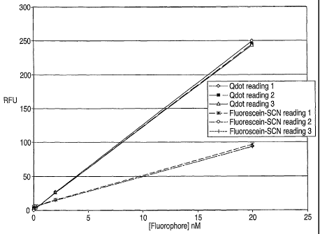
[0030] Figure 1 is a graph of the relative fluorescence versus
concentration of luminescent semiconductor nanocrystals and a typical
fluorophore.
DETAILED DESCRIPTION OF THE PREFERRED EMBODIMENTS
[00311 The practice of the present invention will employ, unless
otherwise indicated, conventional techniques of synthetic organic
chemistry, biochemistry, molecular biology, and the like, which are within
the skill of the art. Such techniques are explained fully in the literature.
See, e.g., Kirk-Othmer's Encyclopedia of Chemical Technology; House's
Modern Synthetic Reactions; the Marvel et al. text ORGANIC SYNTHESIS;
Collective Volume 1, and the like.
-11-
CA 02498003 2010-09-15
WO 2004/023118 PCT/US2003/027715
[0032] While the invention has been described with reference to a
particularly preferred embodiment, it will be appreciated that modifications
can be made without departing from the spirit of the invention. Such
modifications are intended to fall within the scope of the appended
claims.
[0033] In describing the present invention, the following terms will be
employed, and are intended to be defined as indicated below.
[00341 The terms "semiconductor nanocrystal" and "quantum dot" are
used interchangeably herein and refer to an inorganic crystallite between
about 1 nm and about 1000 nm in diameter or any integer or fraction of
an integer therebetween, preferably between about 2 nm and about 50
nm or any integer or fraction of an integer therebetween, more preferably
about 2 nm to about 20 nm (such as about 2, 3, 4, 5, 6, 7, 8, 9, 10, 11,
12, 13, 14, 15, 16, 17, 18, 19, or 20 nm).
[0035] A semiconductor nanocrystal is capable of emitting
electromagnetic radiation upon excitation (i.e., the semiconductor
nanocrystal is luminescent) and includes a "core" of one or more first
semiconductor materials, and may be surrounded by a "shell" of a second
semiconductor material. A semiconductor nanocrystal core surrounded by
a semiconductor shell is referred to as a "core/shell" semiconductor
nanocrystal. The surrounding "shell" material will preferably have a
bandgap energy that is larger than the bandgap energy of the core
material and may be chosen to have an atomic spacing close to that of
the "core" substrate. The core and/or the shell can be a semiconductor
material including, but not limited to, those of the group II-VI (ZnS, ZnSe,
ZnTe, CdS, CdSe, CdTe, HgS, HgSe, HgTe, MgS, MgSe, MgTe, CaS,
CaSe, CaTe, SrS, SrSe, SrTe, BaS, BaSe, BaTe, and the like) and Ill-V
-12-
CA 02498003 2005-03-07
WO 2004/023118 PCT/US2003/027715
(GaN, GaP, GaAs, GaSb, InN, InP, InAs, InSb, and the like) and IV (Ge, Si,
and the like) materials, and an alloy or a mixture thereof.
[0036] A semiconductor nanocrystal is, optionally, surrounded by a
"coat" of an organic capping agent. The organic capping agent may be
any number of materials, but has an affinity for the semiconductor
nanocrystal surface. In general, the capping agent can be an isolated
organic molecule, a polymer (or a monomer for a polymerization reaction),
an inorganic complex, and an extended crystalline structure. The coat is
used to convey solubility, e.g., the ability to disperse a coated
semiconductor nanocrystal homogeneously into a chosen solvent,
functionality, binding properties, or the like. In addition, the coat can be
used to tailor the optical properties of the semiconductor nanocrystal.
Methods for producing capped semiconductor nanocrystals are discussed
below and is known to those of ordinary skill in the art.
[0037] By "luminescence" is meant the process of emitting
electromagnetic radiation (light) from an object. Luminescence results
from a system which is "relaxing" from an excited state to a lower state
with a corresponding release of energy in the form of a photon. These
states can be electronic, vibronic, rotational, or any combination of the
three. The transition responsible for luminescence can be stimulated
through the release of energy stored in the system chemically or added to
the system from an external source. The external source of energy can
be of a variety of types including chemical, thermal, electrical, magnetic,
electromagnetic, physical or any other type capable of causing a system
to be excited into a state higher than the ground state. For example, a
system can be excited by absorbing a photon of light, by being placed in
an electrical field, or through a chemical oxidation-reduction reaction. The
energy of the photons emitted during luminescence can be in a range
from low-energy microwave radiation to high-energy x-ray radiation.
-13-
CA 02498003 2010-09-15
WO 2004/023118 PCT/US2003/027715
Typically, luminescence refers to photons in the range from UV to IR
radiation.
[0038] "Monodisperse particles" include a population of particles
wherein at least about 60% of the particles in the population, preferably
about 75% to 90% of the particles in the population, more preferably
about 80% to 95% of the particles in the population, most preferably
about 90% to 95% of the particles in the population, or any integer in
between this range, fall within a specified particle size range. A
population of monodispersed particles deviate less than 10% rms (root-
mean-square) in diameter and preferably less than 5% rms. Monodisperse
semiconductor nanocrystals have been described in detail in Murray et at.
(J. Am. Chem. Soc., 115:8706 (1993)); and in the thesis of Christopher
Murray, "Synthesis and Characterization of II-VI Quantum Dots and Their
Assembly into 3-D Quantum Dot Superlattices", Massachusetts Institute
of Technology, September, 1995E
[00391 By use of the term "a narrow wavelength band" or "narrow
spectral linewidth" with regard to the electromagnetic radiation emission
of the semiconductor nanocrystal is meant a wavelength band of
emissions not exceeding about 40 nm, and preferably not exceeding
about 20 nm in width and symmetric about the center, in contrast to the
emission bandwidth of about 100 nm for a typical dye molecule with a
red tail which may extend the bandwidth out as much as another 100
nm. It should be noted that the bandwidths referred to are determined
from measurement of the full width of the emissions at half peak height
(FWHM), and are appropriate in the range of 200 nm to 2000 nm.
[0040] By use of the term "a broad wavelength band," with regard to
the excitation of the semiconductor nanocrystal is meant absorption of
radiation having a wavelength equal to, or shorter than, the wavelength of
-14-
CA 02498003 2005-03-07
WO 2004/023118 PCT/US2003/027715
the onset radiation (the onset radiation is understood to be the longest
wavelength (lowest energy) radiation capable of being absorbed by the
semiconductor nanocrystal). This onset occurs near to, but at slightly
higher energy than the "narrow wavelength band" of the emission. This
is in contrast to the "narrow absorption band" of dye molecules which
occurs near the emission peak on the high energy side, but drops off
rapidly away from that wavelength and is often negligible at wavelengths
further than 100 nm from the emission.
[00411 The term "barcode" as used herein refers to one or more sizes,
size distributions, compositions, or any combination thereof, of
semiconductor nanocrystals. Each size, size distribution and/or
composition of semiconductor nanocrystals has a characteristic emission
spectrum, e.g., wavelength, intensity, FWHM, and/or fluorescent lifetime.
In addition to the ability to tune the emission energy by controlling the
size of the particular semiconductor nanocrystal, the intensities of that
particular emission observed at a specific wavelength are also capable of
being varied, thus increasing the potential information density provided by
the semiconductor nanocrystal barcode system. In preferred
embodiments, 2-15 different intensities may be achieved for a particular
emission at a desired wavelength, however, one of ordinary skill in the art
will realize that more than fifteen different intensities may be achieved,
depending upon the particular application of interest. For the purposes of
the present invention, different intensities may be achieved by varying the
concentrations of the particular size semiconductor nanocrystal attached
to, embedded within or associated with an item, compound or matter of
interest. The "barcode" enables the determination of the location or
identity of a particular item, compound or matter of interest. For
example, semiconductor nanocrystals can be used to barcode
pharmaceutical products, blood samples, donated blood, combinatorial
-15-
CA 02498003 2005-03-07
WO 2004/023118 PCT/US2003/027715
libraries including organic compounds, nucleic acids, proteins, peptides,
sugars, lipids or a combination of any one or more of these.
[0042] By the term "doped metal oxide nanocrystals" refers to a metal
oxide, and a dopant comprised of one or more rare earth elements. For
example, suitable metal oxides include, but are not limited to, yttrium
oxide (Y203), zirconium oxide (Zr02), zinc oxide (ZnO), copper oxide (CuO
or Cu20), gadolinium oxide (Gd203), praseodymium oxide (Pr203),
lanthanum oxide (La203), and alloys thereof. The rare earth element
comprises an element selected from the Lanthanide series and includes,
but is not limited to, europium (Eu), cerium (Ce), neodymium (Nd),
samarium (Sm), terbium (Tb), gadolinium (Gd), holmium (Ho), thulium
(Tm), an oxide thereof, and a combination thereof. As known to those
skilled in the art, depending on the dopant, an energized doped metal
oxide nanocrystal is capable of emitting light of a particular color. For
example, the emission color and brightness (e.g., intensity) of a doped
metal oxide nanocrystal comprising Y203:Eu may depend on the
concentration of Eu; e.g., emission color may shift from yellow to red
with increasing Eu concentration. For purposes of illustration only,
representative colors which may be provided are listed in Table 1.
TABLE 1
Fluorescent Color Dopant
blue thulium
blue cerium
yellow-green terbium
green holmium
green erbium
red europium
reddish orange samarium
orange neodymium
yellow dysprosium
white praseodymium
orange-yellow europium + terbium
orange-red europium + samarium
-16-
CA 02498003 2010-09-15
WO 2004/023118 PCT/US2003/027715
[00431 Methods for making doped metal oxide nanocrystals are known
to include, but are not limited to a sol-gel process (see, e.g., U.S.. Pat.
No. 5,637,258), and an organometallic
reaction. As will be apparent to one skilled in the art, the dopant (e.g.,
one or more rare earth elements) are incorporated into the doped metal
oxide nanocrystal in a sufficient amount to permit the doped metal oxide
nanocrystal to be put to practical use in fluorescence detection as
described herein in more detail. An insufficient amount comprises either
too little dopant which would fail to emit sufficient detectable
fluorescence, or too much dopant which would cause reduced
fluorescence due to concentration quenching. In a preferred embodiment,
the amount of dopant in a doped metal oxide nanocrystal is a molar
amount in the doped metal oxide nanocrystal selected in the range of
from about 0.1 % to about 25%. Doped metal oxide nanocrystals may
=
can be excited with a single excitation light source resulting in a
detectable fluorescence emission of high quantum yield (e.g., a single
quantum dot having at a fluorescence intensity that may be a log or more
greater than that a molecule of a conventional fluorescent dye) and with a
discrete fluorescence peak. Typically, they have a substantially uniform
size of less than 200 Angstroms, and preferably have a substantially
uniform size in the range of sizes of from about 1 nm to about 5 nm, or
less than 1 nm.
[0044] The formation of semiconductor nanocrystals is described in
U.S. Pat. Nos. 5,571,018; 5,505,928; 5,262,357; 5,571,018; and
5,262,357. Moreover, semiconductor nanocrystals are commercially available,
for example, from Evident Technologies of Troy, New York.
-17-
CA 02498003 2010-09-15
WO 2004/023118 PCTIUS2003/027715
[0045] In one embodiment, the nanocrystals are used in a core/shell
configuration wherein a first semiconductor nanocrystal forms a core
ranging in diameter, for example, from about 20 Angstroms to about 100
Angstroms, with a shell of another semiconductor nanocrystal material
grown over the core nanocrystal to a thickness of, for example, 1-10
monolayers in thickness. When, for example, a 1-10 monolayer thick
shell of CdS or ZnS is epitaxially grown over a core of CdSe, there is a
dramatic increase in the room temperature photoluminescence quantum
yield. Formation of such core/shell nanocrystals is described more fully in
a publication entitled "Epitaxial Growth of Highly Luminescent CdSe/CdS
Core/Shell Nanocrystals with Photostability.and Electronic Accessibility,"
by Peng at al., published in the Journal of the American Chemical Society,
Volume 119, Nov. 30, 1997, at pages 7019-7029.
[0046] The semiconductor nanocrystals used in the invention will have
the capability of absorbing radiation over a broad wavelength band. This
wavelength band includes the range from gamma radiation to microwave
radiation. In addition, these semiconductor nanocrystals will have a
capability of emitting radiation within a narrow wavelength band of about
40 nm or less, preferably about 20 nm or less, thus permitting the
simultaneous use of a plurality of differently colored semiconductor
nanocrystal probes with different semiconductor nanocrystals without
overlap (or with a small amount of overlap) in wavelengths of emitted
light when exposed to the same energy source. Both the absorption and
emission properties of semiconductor nanocrystals may serve as
advantages over dye molecules which have narrow wavelength bands of
absorption (e.g. about 30-50 nm) and broad wavelength bands of
emission (e.g. about 100 nm) and broad tails of emission (e.g. another
100 nm) on the red side of the spectrum. Both of these properties of
-18-
CA 02498003 2010-09-15
WO 2004/023118 PCT/US2003/027715
dyes impair the ability to use a plurality of differently colored dyes when
exposed to the same energy source.
[00471 Furthermore, the frequency or wavelength of the narrow
wavelength band of light emitted from the semiconductor nanocrystal
may be further selected according to the physical properties, such as size,
of the semiconductor nanocrystal. The wavelength band of light emitted
by the semiconductor nanocrystal, formed using the above embodiment,
may be determined by either (1) the size of the core, or (2) the size of the
core and the size of the shell, depending on the composition of the core
and shell of the semiconductor nanocrystal. For example, a nanocrystal
composed of a 3 nm diameter core of CdSe and a 2 nm thick shell of CdS
will emit a narrow wavelength band of light with a peak intensity
wavelength of 600 nm. In contrast, a nanocrystal composed of a 3 nm
core of CdSe and a 2 nm thick shell of ZnS will emit a narrow wavelength
band of light with a peak intensity wavelength of 560 nm. The
preparation of monodisperse CdSe quantum dots has been described in
detail in Murray et al. (J. Am. Chem. Soc., 115:8706 (1993)).
[00481 A plurality of alternatives to changing the size of the
semiconductor nanocrystals in order to selectably manipulate the emission
wavelength of semiconductor nanocrystals exist. These alternatives
include: (1) varying the composition of the nanocrystal, and (2) adding a
plurality of shells around the core of the nanocrystal in the form of
concentric shells. It should be noted that different wavelengths can also
be obtained in multiple shell type semiconductor nanocrystals by
respectively using different semiconductor nanocrystals in different shells,
i.e., by not using the same semiconductor nanocrystal in each of the
plurality of concentric shells.
-19-
CA 02498003 2010-09-15
WO 2004/023118 PCTIUS2003/027715
[00491 The emission wavelength of the semiconductor nanocrystal may
be varied by tailoring the composition, or alloy, of the semiconductor
nanocrystal. As an illustration, a CdS semiconductor nanocrystal, having
an emission wavelength of 400 nm, may be alloyed with a CdSe
semiconductor nanocrystal, having an emission wavelength of 530 nm.
When a nanocrystal is prepared using an alloy of CdS and CdSe, the
wavelength of the emission from a plurality of identically sized
nanocrystals may be tuned continuously from 400 nm to 530 nm
depending on the ratio of S to Se present in the nanocrystal. The ability
to select from different emission wavelengths while maintaining the same
size of the semiconductor nanocrystal may be important in applications
which require the semiconductor nanocrystals to be uniform in size, or for
example, an application which requires all semiconductor nanocrystals to
have very small dimensions.
[00501 Techniques for producing semiconductor nanocrystals that
fluoresce in a narrow spectral distribution of a selected color are
discussed in, for example, Dabbousi et al. (1997) J. Phys. Chem. B
101:9463-9475 and U.S. Patent No. 6,322,901., For example,
CdSe nanocrystals can be
produced that emit light visible to the human eye, so that in combination
with a source of higher energy than the highest energy of the desired
color, these nanocrystals can be tailored to produce visible light of any
spectral distribution. Semiconductor nanocrystals can also be produced
that emit In the ultraviolet and infra red spectral ranges. Examples of
ultraviolet- and infra red-emitting nanocrystals are, e.g., CdS, ZnS and
ZnSe, and InAs, CdTe and MgTe, respectively. The color of light
produced by a particular size, size distribution and/or composition of a
semiconductor nanocrystal may be readily calculated or measured by
methods which will be apparent to those skilled in the art. As an example
-20-
CA 02498003 2005-03-07
WO 2004/023118 PCT/US2003/027715
of these measurement techniques, the band gaps for nanocrystals of
CdSe of sizes ranging from 1 2 Angstroms to 1 15 Angstroms are given in
Murray et al. J. Am. Chem. Soc. 115:8706 (1993). These techniques
allow ready calculation of an appropriate size, size distribution and/or
composition of semiconductor nanocrystals and choice of excitation light
source to produce a nanocrystal capable of emitting light device of any
desired wavelength.
[00511 Dabbousi et al. also discloses a method that can be used for
overcoating nanocrystals composed of CdS, CdSe, or CdTe with ZnS,
ZnSe, or mixtures thereof. Before overcoating, a nanocrystal core is
prepared by a method described in Murray et al. that yields a substantially
monodisperse size distribution. These methods can be used to prepare
separate populations of semiconductor nanocrystals, wherein each
population exhibits a different characteristic photoluminescence spectrum.
[0052] The present invention provides a method for determining and/or
quantifying the movement of a fluid from one container to another. The
methods of the present invention, by way of example, can (1) detect the
presence and amounts of reagent transferred into a reactor vessel, e.g.,
verifying the addition of appropriate amounts of a reactant into a reaction
vessel to form a chemical product; (2) localize a chemical compound, e.g.,
determination of whether and how much of an addition product is present
in a subsequent processing step or product, such as for use in high
volume screening of nucleic acid testing or in blood testing; (3) detect the
removal of fluid from a container, e.g., verifying or quantifying the
cleaning of a fermentor or bioreactor and determining the presence,
identity, and quantity of residual elements; (4) quantify the dilution of a
composition, e.g., verifying that a primary standard solution has been
diluted to a predetermined concentration; (5) monitor liquid transport,
e.g., monitoring liquid transport in hydraulic systems; (6) evaluate and
-21-
CA 02498003 2005-03-07
WO 2004/023118 PCT/US2003/027715
verify microfluidic dilutions, volume samplings, and other critical fluidic
manipulations; and/or (7) monitor and quantify the amounts of solid
materials that are dissolved in a fluid.
[0053] The method of the present invention includes adding a
fluorescent semiconductor nanocrystal having a defined characteristic
spectral emission based on the physical properties of the semiconductor
nanocrystal, which is tunable to a desired energy by selection of the
particle size, size distribution and composition of the semiconductor
nanocrystal, to a first fluid composition. When the first fluid composition
containing the semiconductor nanocrystal is transferred to a second fluid
composition, the presence and amount of the semiconductor nanocrystal,
and therefore the presence and amount of the first fluid in the second
fluid, can be detected by optically monitoring the emission of the
semiconductor nanocrystal and determining the relative fluorescence as is
understood in the art.
[0054] In one embodiment of the present invention, semiconductor
nanocrystals may be added to a first fluid composition. To measure,
determine, and quantify the presence and amount of the first fluid in a
second fluid composition when the first fluid composition has been
transferred into the second fluid composition, the semiconductor
nanocrystal present in the second composition, by virtue of the transfer of
the first composition into the second composition, may be
spectroscopically viewed or otherwise detected, for example, by
irradiation of the composition with an excitation light source to determine
the presence and quantity of the first composition in the second
composition.
[0055] Since the semiconductor nanocrystal emits a characteristic
emission spectrum based on the selection of the particle size, size
distribution and composition of the semiconductor nanocrystal which can
-22-
CA 02498003 2005-03-07
WO 2004/023118 PCT/US2003/027715
be observed and measured, the quantity of the first composition
transferred into the second composition can be determined. For example,
by knowing the amount of semiconductor nanocrystal in the first solution,
true volume verification of the liquid transfer can be determined by
analyzing the existence and amount of the semiconductor nanocrystals,
which were originally present in the first composition, in the second
composition. Likewise, the extent of fluid transfer can be determined by
quantifying the ratio of semiconductor nanocrystals present in the second
composition to the semiconductor nanocrystals present in the first
composition.
[0056] For example, if a first composition contains 100 semiconductor
nanocrystals/ml and 2.5 ml of the first composition is transferred into a
second fluid composition, the transfer of the first fluid can be detected by
the presence of the homogeneously distributed semiconductor
nanocrystals whereas the quantity of the first fluid delivered into the
second fluid can be verified by measuring the amount of semiconductor
nanocrystals in the second composition. In this example, if the second
composition contains 245 semiconductor nanocrystals it can be quantified
that 2.45m1 of the first composition (or 98%) was delivered to the second
composition. This method has particular application in, for example, high
volume nucleic acid screening assays as a technique to verify reaction
delivery. One of the attributes of the semiconductor nanocrystals is that
they can be constructed to luminescence in regions of the spectrum
outside the normal visible range, in particular, the near infrared region of
the electromagnetic spectrum. This allows for the use of the
semiconductor nanocrystals as tracers in opaque solutions in the visible
region of the spectrum. An example of such a solution is whole blood.
Others examples include bioreactor media, disrupted mixtures of cells,
and other liquid media opaque to visual inspection.
-23-
CA 02498003 2005-03-07
WO 2004/023118 PCT/US2003/027715
[00571 Nucleic acid testing ("NAT") detects very small amounts of
genetic material by copying the target nucleic acid numerous times,
resulting in, for example, a billion-fold amplification of the target. For
example, NAT can detect ribonucleic acid (RNA) from HIV-1 and HCV
when tested in pools of 16 biological samples obtained from multiple
donors. It can also be used to test biological samples from individuals
and label and identify DNA, RNA and nucleotides. In quantitative
applications of repetitive amplifications technologies such as PCR, the
amplification outcomes are dependent upon the initial conditions.
Therefore, verifying the actual concentration of a nucleic acid component
relative to previous concentration conditions in a time synchronous or
non-synchronous replicate prior to amplification can have significant
implications on assay reproducibility. The use of the semiconductor
nanocrystals provides a useful way improve the certainty of
concentrations and therefore the precision of the assay.
[00581 In an alternative embodiment, the present invention includes
adding a fluorescent semiconductor nanocrystal having a defined
characteristic spectral emission based on the physical properties of the
semiconductor nanocrystal, which is tunable to a desired energy by
selection of the particle size, size distribution and composition of the
semiconductor nanocrystal, to a first fluid composition having solid
materials dissolved therein. Many chemical and biological materials are
purified as aqueous solutions or when dissolved in a variety of organic
solvents. Through a series of manipulations of these solutions, such as,
for example, chromatography, electroporetic separations, elutions,
dialysis, and the like, the target component is separated from
contaminants and obtained as a purified material in solution. Chemically
inert semiconductor nanocrystals can be homogeneously dispersed at a
known concentration into the purified solution. After Iyophilization, the
-24-
CA 02498003 2005-03-07
WO 2004/023118 PCT/US2003/027715
semiconductor nanocrystals would remain homogeneously dispersed in
the solid product and could serve to identify and quantify the amount of
solid added to make a subsequent solution. This method is particularly
useful for primary standards that are frequently provided as lyophilized
materials (for stability reasons) and provides improved precision when
preparing initial stock solutions (as well as the subsequent dilutions).
Moreover, by specifically labeling a component to be purified in the crude
state with semiconductor nanocrystals (in such a way as to not interfere
with the chemical or biological activity), it is possible to track the
increasing purity of the material as it is taken through the various
purification manipulations.
[00591 In an alternative embodiment, the measurement, determination
and quantification of the presence and amount of the first fluid in a
second fluid composition may be determined by taking a unit sample of
the second composition and spectroscopically viewing or otherwise
detecting, for example, by irradiation of the unit sample with an excitation
light source to determine the presence and quantity of the semiconductor,
nanocrystal in the unit sample.
[00601 In yet another embodiment of the present invention, it is
possible to measure, determine and quantify the presence and amount of
a plurality of sequentially or batch added fluids in a final fluid composition
when the plurality of fluid compositions include different semiconductor
nanocrystals based on a selection of the particle size, size distribution and
composition of the semiconductor nanocrystal. Thus, for example, a first
composition to be added to the final composition may include
semiconductor nanocrystals which emit a first emission spectrum which is
either spectroscopically viewed or otherwise detected, for example, by
irradiation of the composition with an excitation light source. A second
composition to be added to the final composition may include
-25-
CA 02498003 2005-03-07
WO 2004/023118 PCT/US2003/027715
semiconductor nanocrystals which emit a second emission spectrum
based on the particle size, size distribution and composition of the
semiconductor nanocrystal. A third composition to be added to the final
composition may include semiconductor nanocrystals which emit a third
emission spectrum, and the like. The quantity of the first, second, third,
etc. compositions transferred into the final composition can be determined
by analyzing the existence and amount of the respective semiconductor
nanocrystals in the final composition which were originally present in the
first, second, third, etc. compositions. Likewise, the extent of fluid
transfer from the plurality of compositions into the final composition can
be determined by quantifying the ratio of semiconductor nanocrystals
present in the final composition to the semiconductor nanocrystals
present in the plurality of compositions. The emission spectra of a
population of semiconductor nanocrystals have linewidths as narrow as
25-30 nm. The combination of tunability, narrow linewidths, and
symmetric emission spectra without a tailing region provides for high
resolution of multiply-sized nanocrystals, e.g., populations of
monodisperse semiconductor nanocrystals having multiple distinct size
distributions.
[00611 In the alternative, the quantity of the first, second, third, etc.
compositions transferred into the final composition can be determined by
analyzing the existence and amount of the respective semiconductor
nanocrystals in a unit sample taken from the final composition.
[0062] In another alternative embodiment, the semiconductor
nanocrystal contains a linking agent that is introduced into an
environment containing a chemical/biological target to be marked whereby
the semiconductor nanocrystal is linked with the target by the linking
agent. Linking semiconductor nanocrystals to chemical or biological
targets is known in the art as illustrated by, for example, U.S. Patent Nos.
-26-
CA 02498003 2005-03-07
WO 2004/023118 PCT/US2003/027715
5,990,479; 6,207,392; 6,114,038; 6,221,602; and 6,235,540, which
are herein incorporated by reference. After the composition is transferred
to a subsequent composition, the semiconductor nanocrystal:target
complex may be spectroscopically viewed or otherwise detected, for
example, by irradiation of the complex with an excitation light source to
determine the presence of the chemical/biological target. Since the
semiconductor nanocrystal emits a characteristic emission spectrum
which can be observed and measured, the quantity of the
chemical/biological target transferred can be determined. For example, by
knowing the amount of semiconductor nanocrystal in the first solution,
the true volume verification of the liquid transfer can be determined by
verifying that the semiconductor nanocrystals present in the first
composition are present, in their entirety, in the second composition.
Likewise, the extent of fluid transfer can be determined by quantifying the
ratio of semiconductor nanocrystals present in the second composition to
the semiconductor nanocrystals present in the first composition.
[0063] The present invention is also directed to monitoring fluid
transport. Fluid transport can be measured in a batch or continuous
process by sampling the fluid flow and measuring the amount of
semiconductor nanocrystals present in the unit sample. This method has
particular application in, for example, the monitoring of liquid transport in
hydraulic systems, and evaluation and verification of microfluidic
dilutions, volume samplings and other critical fluidic manipulations.
[0064] In another embodiment of the present invention, the
semiconductor nanocrystals are used to evaluate and verify microfluidic
dilutions, volume samplings, and other critical fluidic manipulations. In
microfluidic systems acts of valving, fluid diversion and sampling are
most commonly done by changing the pumping rate, charge gating and
fluid intersections, or by intermittent or continuous manual modifications
-27-
CA 02498003 2005-03-07
WO 2004/023118 PCT/US2003/027715
of fluid routes. Currently there is no way to verify that those commands
to the liquid system elements have been executed properly. Adding a
semiconductor nanocrystal to a microfluidic system would allow for the
precise evaluation and verification of microfluidic dilutions, volume
samplings, and other critical fluidic manipulations.
[00651 In another embodiment of the present invention, the
semiconductor nanocrystals are used to determine and quantify the
dilution of a first composition. By adding a semiconductor nanocrystal to
a first solution exact dilutions of the solution can be prepared by
measuring and quantifying the presence in the diluted composition of the
semiconductor nanocrystals. For example, if a first solution contains 100
semiconductor nanocrystals homogeneously dispersed per unit volume the
solution can be diluted by exact standards by measuring the
semiconductor nanocrystals in the diluted composition. Thus, by
example, a solution containing ten semiconductor nanocrystals has been
diluted ten-fold. Due to the sensitivity of the semiconductor nanocrystals,
diluted solutions can be made which can be diluted to the order of 1,000
to 100,000, depending on the beginning concentration of semiconductor
nanocrystals. This method has particular application in, for example, the
preparation of primary standards in which exact, traceable volume
additions are required.
[00661 In another embodiment of the present invention, semiconductor
nanocrystals are added to a container, such as a reaction vessel, during a
phase of the reaction. Once the reaction product is obtained, the reaction
vessel is cleaned during a first cleaning iteration. Following the first
cleaning iteration, the reactor vessel is spectroscopically viewed or
otherwise irradiated with an excitation light source to determine the
presence and quantity of the semiconductor nanocrystal present in the
reactor vessel. The presence and amount of the semiconductor
-28-
CA 02498003 2005-03-07
WO 2004/023118 PCT/US2003/027715
nanocrystals provides information on the degree to which the reactor
vessel has been cleaned. The reactor vessel can thereafter undergo
further cleaning iterations, with subsequent detection and quantification
of the semiconductor nanocrystals, until the reactor vessel is cleaned to a
specified degree. This method has particular application in, fermentation
and bioreactor.
[0067] The determination of the degree of cleanliness of the reactor
enables verification of the degree of residual components removed.
Moreover, allowing quantification of the degree of cleanliness of a reactor
would enable a single reactor to be used for a variety of reaction
products. This is especially important in the production of
pharmaceuticals and biomolecular products where the cost of separate
production facilities can be prohibitive. In addition, being able to use the
same reactor for several different pharmaceutical or biomolecular products
would enable a reactor to be used for different pharmaceutical or
biomolecular products, depending upon the needs of patients for a
particular pharmaceutical or the application requirements for a particular
biomolecular product.
[0068] Luminescent semiconductor nanocrystals are useful at low
concentrations of fluids when mixed with larger volume solutions.
Luminescent semiconductor nanocrystals can track the addition of small
volumes of material into large volumes of diluent where the differences
between the luminescent semiconductor nanocrystal and the diluent could
be as large as one part in one million or higher. Similarly, remainders of
solutions as small as one nanoliter from one mL could be detected by the
use of semiconductor nanocrystals. The use of luminescent
semiconductor nanocrystals in volumes as small as 1-10 nL added to 1.0
mL could be confirmed. Moreover, due to the lack of self quenching by
luminescent semiconductor nanocrystals, concentrations up to 20 uM
-29-
CA 02498003 2005-03-07
WO 2004/023118 PCT/US2003/027715
could be employed which would give a dilution linear range of 9 logs.
This would mean that a 1 pL addition or remnant could be quantified in a
1 mL total volume. Self quenching and the innately nonlinear response
would limit the utility of typical chemical fluorophores
[0069] The following Examples serve to illustrate the invention. The
Examples should not be construed to limit the present invention, but
instead serve to illustrate preferred embodiments thereof.
[0070] A dilution analysis was performed to evaluate the optical
properties of luminescent semiconductor nanocrystals relative to a
standard fluorophore, fluorescein isothiocyanate. Luminescent
semiconductor nanocrystals, 655 Q-Dot commercially available from
Quantum Dot Corporation of Hayward, California with an emission
maximum of 655 nm, were stimulated to fluoresce by light at
approximately 450 nm. The fluorescein isothiocyanate emitted light at
approximately 405 nm when stimulated at 395 nM. A solution of
luminescent semiconductor nanocrystals and fluorophore were both
adjusted to a concentration of 20 nM and diluted serially through six logs.
The emission of both the luminescent semiconductor nanocrystals and the
fluorescein isothiocyanate were observed and quantified. As can be seen
from Figure 1, the luminescent semiconductor nanocrystals provided a
significantly more linear response through this dilution sequence than the
standard fluorophor, fluorescein isothiocyanate. This is shown by the
dilution sequence over 6 logs, intercepting at zero. Three separate tests
were run. As can also be seen from Figure 1, the luminescent
semiconductor nanocrystals are approximately 2.5 times more brilliant
than the typical fluorophore, fluorescein isothiocyanate.
[0071] While the invention has been described with reference to
particularly preferred embodiments, it will be appreciated that
modifications can be made without departing from the spirit of the
-30-
CA 02498003 2005-03-07
WO 2004/023118 PCT/US2003/027715
invention. Such modifications are intended to fall within the scope of the
appended claims.
-31-