Note: Descriptions are shown in the official language in which they were submitted.
CA 02498592 2005-03-10
2002P19468WOCA PCT/EP2003/008559
1
Description
Method and circuit arrangement for synchronization of synchro-
nously or asynchronously clocked processing units
In telecommunication systems, Data Centers and other high-
availability systems in many cases as many as several hundred
processor boards are used to provide the required processing
power. Such a processor boards typically consists of a proces-
sor or a CPU (Central Processing Unit), a chip set, main mem-
ory and periphery.
The likelihood of a hardware defect occurring on a typical
processor board within any one year is a single-digit percent-
age figure. Because of the large number of processor boards
grouped together to form a system this means that within a
given year there is a very high likelihood, unless suitable
precautions are taken, of a given hardware component failing
with this type of individual failure, possibly resulting in
the failure of the entire system.
High system availability is demanded for telecommunication
systems in particular and increasingly for Data Centers too.
This figure is typically expressed as a percentage or the
maximum permissible downtime per year is specified. Typical
requirements are for example an availability of >99.999~ or a
non-availability of a few minutes per year at most. Since, in
the case of a hardware defect, the exchange of a processor
board and the restoration of the service usually takes some
time, ranging from 10 minutes or more through to several
hours, the corresponding precautions must be taken at system
level for the event of a hardware defect in order to be able
to meet the request for system availability.
' CA 02498592 2005-03-10
2002P19468WOCA PCT/EP2003/008559
2
Known solutions for meeting such high system availability re-
quirements make provision for there to be redundant system
components. The known methods can be subdivided into two
groups: Software-based methods and hardware-based methods
With software-based methods middleware is typically employed.
The software-based solution however has been shown to be less
flexible since only the (application) software which has been
specifically developed for this particular redundancy scheme
can be used in such a system. This considerably reduces the
range of (application) software which can be used. Over and
above this, the development of application software for soft-
ware redundancy principles demands a very large amount of ef-
fort in practice, with the development also involving a com-
plicated test procedure.
The basic principle underlying the hardware-based method is
that of encapsulating the redundancy at hardware level so that
this is transparent for the software. The major advantage of a
redundancy administered by the hardware itself is that the ap-
plication software is not affected by the redundancy principle
and thus in most cases any given software can be used.
A principle which occurs frequently in practice for hardware
fault-tolerant systems, for which redundancy is transparent
for the software, is what is referred to as the lockstep prin-
ciple. Lockstep means that identically-constructed hardware,
for example two boards, operates clock-synchronously in the
same way. Hardware mechanisms ensure that the redundant hard-
ware, at any given point in time, experiences identical input
stimuli and must thus arrive at identical results. The results
of the redundant components are compared, if they differ an
error is identified and suitable measures are
~
. CA 02498592 2005-03-10
2002P19468WOCA PCT/EP2003/008559
3
initiated (signaling of alarms to operating personnel, partial
or complete safety shutdown, system restart).
The fundamental requirement for the implementation of a lock-
step system is the deterministic timing behavior of all compo-
nents contained in the board, i.e. CPUs, chip sets, main mem-
ory etc. Deterministic timing behavior means in this case that
these components deliver identical results at identical timing
points in a fault-free situation when the components receive
identical stimuli at identical timing points. Deterministic
timing behavior also requires the use of a clock-synchronous
interface. In many cases asynchronous interfaces cause a de-
gree of timing imprecision in the system, which means that the
overall clock-synchronous behavior of the system cannot be
maintained.
For chip sets and CPUs in particular asynchronous interfaces
offer technological benefits for increasing performance, in
which case clock-synchronous operation in accordance with the
lockstep method becomes impossible. In addition modern CPUs
increasingly use mechanisms which make clock-synchronous op-
eration impossible. These are for example internal correction
measure not visible form outside, e.g. correction of an inter-
nal correctable fault on access to the cache memory which can
lead to a very slight delay in instruction processing, or the
speculative execution of instructions. A further example is
the future increasing implementation of CPU-internal clock-
free execution units which provide significant advantages in
respect of speed and power dissipation but prevent clock-
synchronous or deterministic working of the CPU.
A functional lockstep arrangement for redundant processors is
known from US Patent Application 5,226,152 in which all the
processors are connected to a logic which synchronizes the
CA 02498592 2005-03-10
4
accesses of the processors to the shared peripherals and makes
possible a functional lockstep operation of the redundant
processors. The logic uses the wait signals of the processors
here.
As regards the processor boards mentioned at the start, this
arrangement, which only has a central logic, has a significant
disadvantage which involves a logic board having to be pro-
vided as well as the processor boards for a specific number of
processor boards, which then controls the synchronization of
the peripheral accesses. These logic boards would then have to
be monitored in their turn, which would lead to complex moni-
toring mechanisms.
In other words, while the arrangement according to US
IS 5,226,152 appears suitable for providing a functional lockstep
for single-board systems with a number of processors, this ar-
rangement is not suitable for systems with a number of identi-
cal processor boards of the type mentioned at the start.
Further, from US Patent Application 5,353,436, a functional
lockstep arrangement for redundant processors is known in
which each processor is assigned a sync logic circuit, a
counter element for counting the processor events and a com-
parator circuit, which undertake the synchronization of the
processors and allow functional lockstep operation of the re-
dundant processors. The logic circuits likewise use the wait
signals of the processors here.
The comparator circuits are coupled to each other. If inter-
rupts occur the comparator circuits compare the value of the
local event counter in each case with the values of the other
event counters of the arrangement and signal in each case to
the local sync. logic circuit the relation of the local event
counter value to the other event counters of the
AMENDED SHEET
' CA 02498592 2005-03-10
4A
arrangement.
In other words parameters are exchanged between the sync.
logic circuits which characterize the program execution status
of the individual processors. Checking the processor transac-
tions which initiate the synchronization for equality between
den individual processors is however not possible in this
case.
One object of the present invention is thus to specify a
method and an arrangement which makes possible functional
lockstep operation and simultaneously allows the processor
transactions needed for synchronization of redundant proces-
sors to be checked for equality and validated.
This object is achieved by a method for synchronization of
synchronously or asynchronously clocked processing units in
accordance with the features of the Patent Claim 1 and a cir-
cuit arrangement for synchronization of synchronously or asyn-
chronously clocked processing units in accordance with the
features of Patent Claim 17.
Preferred embodiments are the object of the dependent claims.
AMENDED SHEET
CA 02498592 2005-03-10
In accordance with the invention a method is provided for syn-
chronization of identical or different, redundant processing
units PROo, PRO1 which process identical instruction sequences
5 and are clocked synchronously or asynchronously, in accordance
with which active transactions outside the processing units
PROo, PRO1 are used by the blocks EQo, EQ1 assigned by the proc-
essing units PROo, PRO1 for synchronization of the processing
units PROo, PROl,wherein the processing units are delayed in
each case by the assigned blocks and thereby equalized until
the instruction processing of all processing units has reached
the current transaction, with the blocks EQo, EQ1 transferring
parameters via connections Lo, L1 for synchronization of the
processing units PROo, PRO1 which characterize the transac-
tions .
In this case the following transactions can be used for syn-
chronization:
- Non-cacheable memory transactions relating to a local mem-
ory MEMO, MEM1 assigned to the relevant processing units
PROo, PRO1 and/or
- input/output transactions to input/output blocks I/Oo,
I/O1 and/or
- Memory-mapped input/output transactions to external regis-
ters REGo, REG1 and/or
- Non-cacheable memory transactions relating to a common
memory CMEM of the processing units PROo, PRO1.
Read transactions can be executed in this case by the block
assigned to a processing unit leaving the processing units in
the wait state until the arrival of the data to be read and
sending the parameter or parameters of the read transaction to
the block most directly linked to the transaction destination
I/0o, I/O1, MEMO, MEM1, REGo, REG1, CMEM, with the block linked
most directly to the transaction destination receiving the
AMENDED SHEET
CA 02498592 2005-03-10
5a
parameter or parameters of the other blocks as well as the lo-
cally generated parameter or parameters and comparing them
and, if they match, executing the read transaction and dis-
tributing the read data to all blocks, whereon all blocks forward
AMENDED SHEET
2002P19468WOCA CA 02498592 2005-03-10 pCT/EP2003/008559
6
the data read to the assigned processing units and enable
the instruction execution to continue.
Write transactions can be executed by the block assigned to a
processing unit being able to leave the processing unit in the
wait state until the conclusion of the write process and then
sending the parameter or parameters of the write transaction
to the block linked most directly to the transaction destina-
tion I/Oo, I/O1, MEMO, MEM1, REGo, REG1, CMEM, with the block
linked most directly to the transaction destination receiving
the parameter or parameters of the other blocks as well as the
locally generated parameter or parameters and comparing them
and, if they match, executing the write transaction and ac-
knowledging the completed write process to all blocks, whereon
all blocks enable the instruction execution of the assigned
processing units to continue.
Advantageously external events, e.g. interrupts, can be han-
dled in conjunction with the transaction-based synchronization
method according to the invention, if the handling of the ex
ternal events is safeguarded by the reading of a value, e.g.
interrupt vector, from a memory location or of a register and
it is also ensured that all processing units are presented
with the external events for execution at the same point in
the instruction processing. The read transaction initiating
the event handling is executed as described above, e.g. by
means of an Interrupt Acknowledge cycle.
A suitable method for synchronization of external events is
described in European Patent Application 02020602 and provides
for the external events to be cached, with the stored external
events being retrieved in a separate operating mode of the
processing units for processing by at least one execution unit
2002P19468WOCA CA 02498592 2005-03-10 pCT/EP2003/008559
7
of the processing units in each case and where the processing
units in this operating mode respond to the fulfillment of a
condition that can be specified by instructions or is preset
and the continuation of the instruction execution is delayed
by the blocks EQo, EQ1 until all processing units have ended
the separate operating mode.
The change to the separate operating mode is made for example
if comparator elements K of the processing units determine
that counter elements CIC match register elements MIR, with
the content of the register elements MIR being able to be
specified by instructions and being identical for all process-
ing units PROo, PRO1 and the counter element CIC containing the
number of instructions executed by the execution unit since
the last change to the separate operating mode.
IS Error handling can be initiated if the block linked most
closely with the transaction destination detects a deviation
of the parameters of the other blocks as well as of the lo-
cally generated parameter or parameters. The error handling
can stop the transaction to be executed in this case and start
a routine for diagnosis, error isolation and if necessary for
restoring synchronization. If N (e. g. N=3) processing units
are present, an (N-1) out of N majority decision or generally
an (N-M) from N majority decision can then be made and the
processing unit or units showing the discrepancy can be deac-
tivated.
Furthermore a failure detection of individual processing units
can be undertaken in that for a given a transaction, starting
with the earliest availability of the parameter or the parame-
ters for the block of a processing unit, parameters which do
not arrive or which only arrive after a specified time are
discarded and with error handling been initiated for
CA 02498592 2005-03-10
8
processing units with parameters which do not arrive or only
arrive after a predetermined time.
The invention further makes provision for an arrangement for
synchronization of synchronously or asynchronously clocked
processing units PROo, PRO1 of redundant data processing sys-
tems with the following features:
- At least two processing units PROo, PRO1 for processing
identical instruction sequences,
- Peripherals MEMO, MEM1 exclusively assigned to the process-
ing units in each case for saving and/or exchanging data,
- Peripherals I/Oo, I/O1, REGo, REG1, CMEM which can be used
jointly by all processing units for saving and/or exchang-
ing data,
- The blocks EQo, EQ1 assigned to the processing units, with
the blocks EQo, EQ1 featuring a means for monitoring
transactions as well as means for stopping the assigned
processing unit until the current transaction is reached
by all processing units and also means Lo, L1 for trans-
mission to other blocks of parameters characterizing the
transaction.
The blocks EQo, EQ1 can in this case feature means for synchro-
nization of the processing units especially on the basis of
the following transactions:
- Non-cacheable memory transactions relating to a local mem-
ory MEMO, MEM1 assigned to the relevant processing units
PROo, PRO1 and/or
- Input/output transactions for input/output blocks I/Oo,
I/O1 and/or
- Memory-mapped input/output transactions to external regis-
ters REGo, REG1 and/or
- Non-cacheable memory transactions relating to a common
memory CMEM of the processing units PROo, PRO1
AMENDED SHEET
2002P19468WOCA CA 02498592 2005-03-10 p~T/EP2003/008559
8~
15
25
In this case the blocks advantageously feature means for form-
2002P19468WOCA CA 02498592 2005-03-10 pCT/EP2003/008559
9
ing the following parameters representing transactions:
- Input/output addresses and/or
- Memory addresses and/or
- Data to be transferred and/or
- Type of transaction and/or
- A signature formed from the input/output addresses and/or
the memory addresses and/or the data to be transferred
and/or the type of transaction.
For handling external events such as interrupts for example,
the processing units preferably have the following features:
- At least one execution unit EU,
- At least one counter element CIC for counting the in-
structions executed by the execution unit since the last
change to the separate operating mode
- At least one register element MIR for which the contents
can be specified by instructions or is predetermined,
- At least one comparator element K to switch over the exe-
cution unit EU into a separate operating mode responding
to the correspondence of the counter element CIC with the
register element of MIR, with external events cached in
the separate operating mode to be routed to the processor
modules which influence the processor modules being re-
trieved by the processor modules.
The retrieval of the cached external events can advantageously
be undertaken here by means of software, firmware, microcode
or hardware.
A significant advantage of the invention can be seen in the
fact that the use of any new or existing software on a hard-
ware fault-tolerant platform is made possible, in which case
the processing unit supporting the invention can be used in
this platform without there being the requirement for clock-
synchronous, deterministic operation of the CPU.
2002P19468WOCA CA 02498592 2005-03-10 pCT/EP2003/008559
Further advantages are:
- The processing units which are redundant to each other
which typically consist of a CPU, a Northbridge and local
memory, do not have to be operated rigidly coupled in
5 phase to each other.
- The CPUs do not have to be identical which in particular
enables simultaneous use of different CPU steppings
within a redundant system, and they can be operated with
different clock frequencies.
10 - The CPUs can behave differently in relation to the specu-
lative execution of instructions.
- Different CPU-internal execution and times of identical
CPUs, as a result of corrections after the occurrence of
alpha particles which corrupt the data merely lead to the
synchronization events been reached at slightly different
points in time.
The problems described for ensuring a clock-synchronous deter-
ministic operation lead as a result of the timing imprecision
of future CPUs to execution of instructions for which the tim-
ing cannot be precisely correlated. Since the CPU must react
to external events for a typical application, e.g. to an in-
terrupt generated by a peripheral device or to data which is
written by a device into a main memory, it must be ensured
that the CPU knows about these events at identical points in
the instruction execution since otherwise the evaluation of
these events could lead to different program execution se-
quences of redundant CPUs.
The present invention ensures that external events relevant to
the program execution sequence, such as interrupts or data
created by external devices is presented to redundant CPUs at
2002P19468WOCA CA 02498592 2005-03-10 pCT/EP2003/008559
11
identical points in the instruction execution and thereby the
lockstep mode of operation can be emulated.
In addition output events of redundant CPUs which are pre-
sented at identical points in the instruction execution are
compared and the results thereby validated. By contrast with
known methods which effect the synchronization and the distri-
bution of data from the processor periphery using software-
based methods, in accordance with the invention this is done
by hardware. A decisive advantage of this method is that the
effect on performance, compared to software-based methods is
smaller by an order of magnitude. The method described is also
completely transparent for the application and operating sys-
tem software, i.e. existing application and operating system
software can continue to be used without modification.
An exemplary embodiment of the invention is explained in more
detail below in conjunction with three Figures.
Figure 1 shows schematically two processing units with as-
signed periphery and synchronization of transactions.
Figure 2 shows schematically two processing units which on the
basis of their periphery transactions are synchronized by two
blocks.
Figure 3 shows schematically the structure of a preferred
processing unit with further details.
Figure 4 shows a timing diagram of the instruction processing
of two differently clocked processing units as well as their
inventive synchronization.
In Figure 1 two processing units PROo, PRO1 are shown schemati-
cally, for which the externally active transactions are syn-
chronized. As examples transactions for the following compo-
nents are shown: Local memory MEMO, MEM1, registers REGo, REG1
and input/output or I/O blocks I/Oo, I/O1. In this case first
components MEMO, REGo and I/Oo are assigned to the first proc-
12002P19468WOCA CA 02498592 2005-03-10 pCT/EP2003/008559
12
essing unit PROo while the second processing unit PRO1 is as-
signed second components MEM1, REG1 and I/O1. As a shown by the
corresponding dotted line connections, the processing units
have access to the register REG1 and the I/0 block I/Oo, of the
other processing unit in each case, whereas only the assigned
processing unit PROk has access to the local memory MEMk.
In addition an example of a component is shown to which the
processing unity have common access, here, common memory CMEM,
with the common memory, by contrast with the registers and the
I/0 blocks, not being assigned to any of the processing units.
Figure 2 again shows the two processing units and typically
the I/0 blocks as well as the registers from Figure 1. These
are not conventionally connected via the corresponding inter-
faces or interface modules, but by means of equalizer blocks
EQo, EQ1. All accesses of the processing units PROo are re-
ceived by equalizers EQo, processed and forwarded accordingly,
likewise the processing unit PROo is presented with all exter-
nal data and events by the equalizer EQo. Similarly the proc-
essing unit PRO1 is assigned an equivalent equalizer EQ1.
The equalizers EQo, EQ1 exchange information and to this end
advantageously have a fast and direct connection Lo, L1. This
connection can, as shown, be logically and/or physically sub-
divided into a first connection Lo:EQo -> EQ1 and a second con-
nection L1 : EQ1 -> EQo .
As shown by dotted lines in Figure 2, in accordance with the
present invention, a further unit consisting of a processing
unit PRO1 an equalizer EQ and periphery REG1 I/O in each case
can be connected in order to form a corresponding multiply-
redundant system. By adding a further unit of this type a 3-
fold redundant system would be produced in which error han-
dling using a 2-out-of-3 multiple decision could be under-
2002P19468WOCA CA 02498592 2005-03-10 pCT/EP2003/008559
13
taken.
Figure 3 finally shows a more detailed realization of the in-
vention in conjunction with a conventional processor/periphery
architecture of which the outstanding feature is that a cen-
tral processor CPU is coupled via a Northbridge interface unit
NB to a Southbridge interface unit SB, where the Northbridge
e.g. also includes the interface to the local memory MEMO,
whereas the Southbridge for example includes an interrupt con-
trolley and other I/O functions.
As shown by way of example in Figure 3, a processing unit PROo
can be constructed from a CPU, a Northbridge and local memory.
The CPU in an especially advantageous embodiment, in addition
to the conventional units of which only a cache and an execu-
tion unit EU are shown in order to simplify the diagram, can
include a register MIR, a counter CIC and a comparator K, the
purpose of which is to only forward external events such as
interrupts and exceptions at particular points in the instruc-
tion execution and to guarantee an otherwise interruption-free
execution sequence of the processing of sequences of instruc-
tions.
The equalizer in accordance with the invention EQo is prefera-
bly arranged between the Northbridge and the Southbridge,
since the interface between Northbridge and Southbridge fea-
tures all the necessary signal lines which enable the equal-
izer to stop the processing of the instruction sequences until
synchronization of the processing unit PROo with the adjacent
processing units (not shown) is achieved. The diagram only
shows the connections Lo, h1 for connecting
2002P19468WOCA CA 02498592 2005-03-10 pCT/EP2003/008559
14
the equalizer EQo to equalizers of adjacent processing units.
The logical grouping depicted in Figure 3 does not necessarily
correspond to the actual physical grouping of the individual
components. For example the Northbridge can be integrated into
the CPU or the equalizer can be integrated into the
Northbridge or the Southbridge or can be together with the
Northbridge in the CPU.
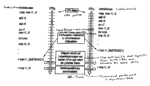
Figure 4 shows a graphic of the synchronization of the in-
struction execution of two processing units in a timing dia-
gram. In the example shown in Figure 4 identical instruction
sequences are processed by the two CPUs CPUo and CPU1, with
CPUo being operated at a lower clock rate than CPU1. CPU1 thus
reaches each instruction at an earlier time than CPUo, provided
that at the beginning, i.e. on processing of the mov rl, r2
instructions, all registers and memory assigned to the CPUs
were synchronized.
This non-synchronous instruction processing is tolerable for
as long as the CPU is not interacting with the outside world,
for example by means of I/0 blocks or access to common memory.
For transactions of this type, in the example shown in Figure
4 the reading out of the I/O registers 0x87654321, it is nec-
essary however for these transactions to take place simultane-
ously for both CPUs and especially with the same result. This
is achieved by means of the equalizers, as described below. At
the same time the equalizers make sure that the synchroniza-
tion of the CPUs is restored at such transaction points.
Following on from the lockstep mode of operation, the method
in accordance with the invention is referred to below as emu-
fated lockstep. One implementation for the emulated lockstep
consists of at least two processing units PROo and PRO1 which
can consist of a CPU, memory and also memory control
2002P19468WOCA CA 02498592 2005-03-10 pCT/EP2003/008559
(Northbridge of a standard chip set). These processing units
are identically constructed but can however feature different
CPUs or different steppings of the CPU, and are started in an
identical state, i.e. identical memory and CPU register con-
5 tents. A coupling using a shared or synchronized clocks is not
required in accordance with the invention.
As part of the machine instruction execution, memory cycles,
for example write cycles, read cycles and if necessary I/0 cy-
cles are initiated by the CPUs. All cycles which fulfill the
10 following conditions are suitable for synchronization of the
CPUs, if necessary with exchange of data between the CPUs:
(a) They are instruction deterministic, i.e. issued identi-
cally by all CPUs at the same point in the program and in the
same sequence, and
15 (b) They are always issued by the CPUs outwards, i.e. they
are always visible and able to be accessed outside the proces-
sors; Processor-internal cache cycles are unsuitable for exam-
ple.
The following memory cycles meet these general conditions for
example:
- Non-cacheable memory cycles in the own memory MEMO, MEM1,
- I/O cycles,
- Memory mapped I/O cycles, with for example an external
register REGo, REG1
- non-cacheable memory cycles to an external common memory
CMEM.
Various external registers, e.g. timers, counters and/or an
interrupt logic, as well as I/0 units to the outside world,
e.g. Ethernet controllers or SCSI controllers, are as a rule
in communication with the CPU. Between CPU and T/0 unit an
equalizer is connected for each CPU via an asynchronous or
synchronous interface which implements the emulated lockstep
2002P19468WOCA CA 02498592 2005-03-10 PC~,/Ep2003/008559
16
method. Between the equalizers EQo, EQ1 asynchronous or syn-
chronous point-to-point data connections Lo, L1 are required so
as to be able to exchange data addresses or signatures. In the
case of transmission errors a repetition of the transmission
can be provided at the asynchronous interfaces.
A read or write access to I/0 units or registers is undertaken
as memory-mapped I/0 or direct I/0. The I/O units are all
visible and accessible via separate memory addresses. By con-
trast the registers can be connected in a master-master or a
master-slave configuration. With the master-master configura-
tion the registers of the processing unit assigned in each
case are accessed for reading or writing. The requirement for
this mode of operation is that registers are in the same state
when accessed by the processing units in order to guarantee
the parallel operation of the units.
With the master-slave configuration exclusively the registers
of the master unit are read by all units and the registers of
the master unit are only written by the master unit. For exam-
ple to read out the current time of day from all units of the
Time-of-Day counter (ToD) of the master unit is used to ensure
that all units, when reading out the ToD counter, are supplied
with exactly the same time of day, i.e. only the registers as-
signed in one processing unit are addressed. Events such as
interrupts for example which take place at other units must
then be transferred to the master unit. Write accesses into
these registers must take place at all units or be stored in
the main memory in shadow registers in order to for operation
to continue in the event of an error with correct data with a
new master unit. This can be controlled either by means of
software or hardware.
2002P19468WOCA CA 02498592 2005-03-10 pCT/EP2003/008559
17
Individual transactions and the synchronization processes oc-
curring as a result of these transactions are described in
greater detail below.
Read transactions
The read instruction of a CPU of a processing unit PRO reads
data out of an I/O unit. Such a read instruction is illus
trated in Figure 4, for example it might be the instruction
load r1, [0x87654321]. This instruction is generated by all
CPUs at the same point in the instruction execution and is di-
rected to a specific I/0 unit, for example I/Oo, or a master
register. The time of the read instruction can however differ
for the CPUs. In Figure 9 CPUo reaches said read instruction
later than CPU1.
The I/O address or memory address generated by the CPU and the
attributes of the transaction, e.g. Memory read or I/0 read or
data length of a signature generated from address and attrib-
utes are sent by the equalizer directly connected to the CPU
to all other equalizers. Only when the equalizer which is con-
nected to the addressed I/0 resource recognizes that the read
request has been generated by all CPUs will the actual read
access be executed. The data rate is distributed for master-
slave configurations to all equalizers which then conclude the
read instruction of the CPU connected in each case by forward-
ing the data to the CPU. The data can arrive at the CPUs at
different points in time but the further program execution is
not adversely affected by this.
Should the I/0 address or signature differ in the equalizer,
either the read access is not executed or an error interrupt
is generated, for example a Non-Maskable Interrupt NMI to the
CPU, or a majority decision, e.g. 2-out-af-3, is taken if a
12002P19468WOCA CA 02498592 2005-03-10 pCT/EP2003/008559
18
configuration with three available CPUs is involved. The
faulty unit is separated and diagnosed.
To detect failures of individual units the timing of the read
accesses is monitored, i.e. the read instructions of all CPUs
must be generated within a certain predetermined time. If this
timespan between the instructions is exceeded a timeout is
generated, the failed unit is separated and diagnosed.
read accesses are processed in the order in which they occur.
There is no provision for them to overtake each other.
Write transactions
The Write instruction writes data into an I/0 unit or a memory
unit. It is generated by all CPUs at the same point in the in-
struction execution and is for example directed to a specific
I/0 unit, e.g. I/Oo. The time of the Write instruction can how-
IS ever differ at the CPUs.
The I/O address, the date and the attributes or the signature
calculated from them generated for example by the CPU are sent
by the directly-connected equalizer to all other equalizers.
Only when the write request has been generated by all CPUs and
has been validated by the equalizer is the actual write access
executed.
Should the I/0 address, the date and/or the attributes or the
signature differ at an equalizer, the write access is either
not executed and an error interrupt is generated, for example
a Non-Maskable Interrupt NMI to the CPU, or a majority deci-
sion, e.g. 2-out-of-3 is taken if a configuration with 3 CPUs
is involved. The faulty unit is separated arid diagnosed.
CA 02498592 2005-03-10
2002P19468WOCA PCT/EP20031008559
19
To detect failures of individual units the timing of the write
accesses is monitored, i.e, the write instructions of all CPUs
must be generated within a certain predetermined time. If this
timespan between the instructions is exceeded a timeout is
generated, the failed unit is separated and diagnosed.
Write accesses are processed in the order in which they occur.
There is no provision for them to overtake each other. It is
however possible for a number of write cycles to be generated
by a CPU (known as Posted Writes). For handling these multi-
ple-write transactions a correspondingly dimensioned first-in-
first-out memory (not shown) can be provided.
Interrupts
The external events influencing the execution sequence of the
program are not routed directly to the CPU but are first
cached by suitably-designed hardware. This hardware can in
this case be a component of a block outside the CPU or a com-
ponent of the CPU itself. The CPU contains a counter CIC (Com-
pleted Instruction Counter) which counts machine instructions
which the CPU has completely executed. The CPU further con-
tains a register MIR (Maximum Instruction Register) into which
information is written by software (ELSO) supporting the emu-
lated lockstep procedure.
Furthermore the CPU features the comparator K which compares
the number of completed instructions, that is the counter CIC,
with the register MIR and, if they are equal generates an in-
terrupt request for example which interrupts instruction exe-
cution after the number of instructions specified by the reg-
ister MIR and switches the CPU into another operating mode. In
this operating mode for example suitable microcode is executed
or a branch is made to an interrupt service routine or hard-
ware signals are used to indicate that a
2002P19468WOCA CA 02498592 2005-03-10 pCT/EP2003/008559
synchronization point has been reached. In this operating mode
the external events are then presented to the redundant CPUs
so that after they leave this operating mode all CPUs can in-
terpret these events in the same way and thus will execute the
5 same instructions in the sequence.
For example, after reaching the number of machine instructions
specified by the register MIR, the CPU branches to an Inter-
rupt Service Routine in which the state of the interrupt sig-
nals kept away by the described hardware of the CPU is inter-
10 rogated such that a redundant CPU which may make this inquiry
at a slightly later point in time obtains the identical infor-
mation. This inquiry is for example a read access to an inter-
rupt register. This read access is handled as described above
which ensures that all CPUs read the same interrupt vector and
15 initiate the same actions.
Before the separate operating mode is left the counter CIC is
reset. Subsequently a branch is made back to the point in the
program at which the interruption occurred when the value for
the counter CIC predetermined by the register MIR was reached.
20 Thereafter the CPU will again execute the number of machine
instructions predetermined by the register MIR and when
counter CIC reaches the register value MIR it will change the
mode and thereby make it possible to accept external events.
For example software ELSO supporting the emulated lockstep op-
eration can set the register MIR to a value of 10,000. A CPU
which is operated at a clock frequency of 5 GHz and on average
executes one machine instruction per clock (length of a clock:
1/200 ps) would thus be interrupted in its instruction execu-
tion after 2 ps and enable synchronization with external
events.
2002P19468WOCA CA 02498592 2005-03-10 pCT/EP20031008559
21
Direct Memory Access DMA
With a DMA (Direct Memory Access) transaction an I/0 unit can
access the main memory directly for reading and writing. The
timing relationship of a access by the I/O units to the CPU is
not specified. If the CPU were to access the same memory area
during a DMA transfer, processing units could lose their
pseudo-synchronous operating mode since the main memory of the
processing units is no longer necessarily identical at the
time of the access.
For a DMA transaction it must thus be ensured that a notifica-
tion is sent to the CPU which arrives at all CPUs at the same
point in the instruction execution. A number of solutions for
this are illustrated below.
- For example the CPUs can be notified by the I/O unit gen-
erating an interrupt after the completion of the DMA
transfer which notifies the CPU that the transfer has been
completed and that the transferred memory area is released
again. As a result of the interrupt the interrupt status
is read by the source, that is the I/0 unit. This reading
via the I/O bus at the units, e.g. the PCI bus, forces a
serialization of the transactions so that data generated
by the I/0 units is in the main memory of all processing
units in a guaranteed sequence.
- In another embodiment an entry can be made by the CPU in a
register on transfer of jobs generated by the CPU of a
processing unit to the I/0 units, which initiates the DMA
transfer. Alternatively scripts or lists, which are simul-
taneously used by both the CPU and also by the I/0 unit
can be present as local memory at the I/O unit. A possible
access by the CPU is then undertaken as a memory-
CA 02498592 2005-03-10
2002P19468WOCA PCT/EP2003/008559
22
mapped read or write instruction, and it is ensured that
all CPUs work with the same data.
In the other direction when a descriptor of the job for
the CPU generated by the I/0 unit or the I/O units is to
be in the main memory of a processing unit PRO and is to
be read out by the CPUs with a polling process, the CPUs
read a so-called I/0 lockout register. Thereafter at least
no write transaction of the I/0 units is sent by the
equalizer into the local main memory of the processing
unit PRO and the write transactions last sent by the I/0
units will be written by the equalizer into the local main
memory of all processing units. This is frequently re-
ferred to as "flushing". This ensures the same contents in
the main memories of all processing units in relation to
write transactions generated by the I/0 units. Subse-
quently the point in the main memory is read by all CPUs
for which the value indicates for example the conclusion
of an I/0 job. Thereafter the I/0 lockout register will be
written to or read from again or an I/0-free register will
be written or read to enable write access to the main mem-
ory again by the I/0 units.
- in a further embodiment the following method can be ap-
plied if the descriptor of the job generated by the CPU or
the CPUs for the I/0 units is to be in the main memory of
the PRO and reading out from the main memory is to be by a
polling method: The CPUs read a so-called I/0 lockout reg-
ister. Thereafter at least no further read transaction of
the I/O units is sent to the main memory of the processing
units. Subsequently a value is written into the memory lo-
ration in the main memory of all CPUs which represents a
trigger or initiator for an I/O job.
CA 02498592 2005-03-10
2002P19468WOCA PCT/EP2003/008559
23
The I/0 lockout register is then read or written again and
an I/0-free register is read or written to again allow
read access to the main memory by the I/O units.
Data comparison
All data which is read by the I/O units from the main memory
is read by all equalizers from the main memory of the con-
nected processing units, completely or as a signature and sent
to the equalizers connected to the requesting I/O unit and
compared by the latter. Alternatively the other equalizers can
also perform a comparison. In the case of equality the data is
forwarded to the I/0 unit If a difference is detected in a ma-
jority decision is made if necessary, e.g. 2-out-of-3, and the
faulty unit is separated and diagnosed.
All data which is generated by the CPUs of the processing
units is sent completely or as a signature to the equalizers
connected to the destination I/0 unit and compared by the lat-
ter. Alternatively the other units can also perform a compari-
son. In the case of equality the data is forwarded to the I/0
unit If a difference occurs a majority decision is made if
necessary, e.g. 2-out-of-3, and the faulty unit is separated
and diagnosed.
All read requests generated by the CPUs of the processing
unit, characterized for example by the read instruction, ad-
dresses and attributes, are sent completely or as a signature
to the equalizer connected to the source and compared by the
latter. Alternatively the other units can also perform a com-
parison. In the case of equality the read transactions are
executed and the data read is sent to all equalizers. If a
difference occurs a majority decision is made
2002P19468WOCA CA 02498592 2005-03-10 pCT/EP2003/008559
24
if necessary, e.g. 2-out-of-3, and the faulty unit is sepa-
rated and diagnosed.
For emulated lockstep, read and write transactions of the CPU
are not compared as regards their local main memory MEM since
this can be entirely different, e.g. because of different
speculative accesses of the CPUs or different cache behavior.
To check the contents of the memory areas of the various proc-
essing units PRO for equality, a check must be initiated, by a
routining software for example at a point in time at which it
can be in short that the memory contents is in a consistent
fault-free state and remains consistent for the duration of
the checking. The memory checking itself can be undertaken by
software, i.e. the software/CPU reads a memory area for exam-
ple, forms a checksum and compares the checksums determined
from the different processing units. The memory checking can
also be undertaken by hardware in that facilities arranged in
the equalizers read the memory of the connected processing
units, form checksums and compare them with each other.
Multiprocessor network architecture with shared memory
Emulated lockstep operation is suitable for synchronizing mem-
ory accesses by a number of processing units to a common mem-
ory CMEM and for performing a data comparison like the one de-
scribed above, provided that the transactions fulfill the gen-
eral conditions explained at the start; For example non-
cacheable memory transactions.
This means that it is possible in a further development to de-
fine multiprocessor configurations which consist of a number
of processing units (with local memories) which can all access
a common memory CMEM. In this case each processor unit is du-
plicated for reasons of redundancy and for error detection,
2002P19468WOCA CA 02498592 2005-03-10 PCT/EP2003I008559
i.e. a processor unit consists of two identical processing
units PRO (not shown) which in the way described above execute
all tasks in parallel and synchronize themselves on access to
a common memory and in doing so perform a data comparison.