Note: Descriptions are shown in the official language in which they were submitted.
2002P20142WOUS PCT/EP2003/008794
CA 02498596 2005-03-10
1
Description
Method for event synchronization, especially for processors of
fault-tolerant systems
In many cases up to several hundred processor boards are used in
telecommunication systems, data centers and other highly available
systems, to provide the necessary computing power. Such a processor
board typically comprises a processor or CPU (Central Processing
Unit), a chip set, main memory and peripheral modules.
The probability of a hardware defect occurring per year in a
typical processor board is in the single digit percentage range.
The large number of processor boards combined in a system means
that over the period of one year there is a very high probability
of failure of any hardware component, whereby such an individual
failure can result in failure of the entire system, if appropriate
precautions are not taken.
A high level of system availability is a requirement for
telecommunication systems especially and also increasingly for data
centers. System availability is expressed as a percentage for
example or the maximum permissible downtime per year is specified.
Typical requirements are for example an availability of >99.999% or
a non-availability of maximum several minutes during the year. As
it generally takes a time in the range of several tens of minutes
to several hours to replace a processor board and restore the
service in the event of a hardware defect, precautions have to be
taken for the event of a hardware defect at system level, in order
to be able to comply with system availability requirements.
2002P20142wOUS PCT/EP2003/008794
CA 02498596 2005-03-10
2
Known solutions for compliance with such stringent system
availability requirements provide for redundant system components.
The known methods can be divided into two main groups: software-
based methods and hardware-based methods.
In the case of software-based methods a form of middleware is
typically used. The software-based solution however proves not to
be very flexible, as only the (application) software developed for
the particular redundancy scheme can be used in such a system. This
limits the range of useable (application) software significantly.
Also the development of application software for software
redundancy principles in practice requires a great deal of time and
effort with the development also entailing a complicated test
method.
The basic principle of hardware-based methods is based on
encapsulating redundancy at hardware level so that it is
transparent for the software. The essential advantage of redundancy
managed by the hardware itself is that the application software is
not impaired by the redundancy principle and therefore in most
instances any software can be used.
A principle frequently encountered in practice for hardware-fault-
tolerant systems, the redundancy of which is transparent for the
software, is what is known as the lockstep principle. Lockstep
means that identically structured hardware elements, e.g. two
boards, are operated in the same manner with clock-controlled
synchronism. Hardware mechanisms ensure that the redundant hardware
experiences identical input stimuli at a defined time and therefore
has to supply identical results. The results of the redundant
components are compared and if there is a difference, a fault is
determined and appropriate measures are initiated
2002P20142WOUS PCT/EP2003/008794
CA 02498596 2005-03-10
3
(operator alarm, partial or total security shutdown, system
restart).
The basic condition for the implementation of a lockstep system is
the clock-based deterministic behavior of all the components
contained in the board, such as CPUs, chip sets, main memory, etc.
Clock-based deterministic behavior here means that said components
supply identical results at identical clock times, if the
components receive identical stimuli at identical clock times.
Clock-based deterministic behavior also assumes the use of
interfaces in clock-controlled synchronism. Asynchronous interfaces
cause a certain temporal indeterminacy in the system in many
instances, whereby the entire synchronized behavior of the system
cannot be maintained.
However for chip sets and CPUs specifically asynchronous interfaces
offer technological advantages with an increase in capacity, as a
result of which operation in clock-controlled synchronism according
to the lockstep method becomes impossible. Also modern CPUs
increasingly use mechanisms, which prevent operation with clock-
controlled synchronism. These are for example internal corrective
measures, not visible externally, e.g. correction of an internally
correctable fault with access to the cache, which can result in a
slight delay in command processing or the speculative execution of
commands. A further example is the increasing implementation in the
future of CPU-internal clock-free execution units, allowing
significant advantages with regard to speed and power dissipation
but preventing operation of the CPU in clock-controlled synchronism
or a deterministic manner.
European patent application 02020602 discloses a method for
synchronizing external events, which are supplied to a CPU and
influence the same, according to which the external events are
2002P20142WOUS PCT/EP2003/008794
CA 02498596 2005-03-10
4
stored in an intermediate manner, whereby the stored external
events are retrieved in a separate operating mode of the CPU for
processing by an execution unit and whereby in this operating mode
the CPU enters into compliance with a condition that can be
predefined by commands or is predefined in a permanent manner. This
method is also referred to as "emulated lockstep operation".
EP 02020602 advantageously provides for the change to separate
operating mode being executed, if a comparator element of the CPU
determines the correspondence of a counter to a Maximum Instruction
Register (MIR), whereby the content of the MIR can be predefined by
commands and the counter contains the number of instructions
executed by the execution unit since the last change to separate
operating mode.
However modern CPUs cannot be interrupted so that they stop after a
precise number of instructions. The reason for this is that a
plurality of instructions can be processed in parallel, which are
terminated at a common time. Therefore for example in one clock
pulse 99 instructions can be processed on all redundant CPUs, in
the next clock pulse there are for example 100 instructions on one
CPU due to a difference in execution while on another there are 101
instructions. An external event, e.g. an interrupt, can therefore
not be presented at identical points in the command execution.
One object of the present invention is to specify a method, with
which external events can also be presented at identical points in
the command execution of redundant CPUs, even if it is not
definitely possible to interrupt the redundant CPUs after execution
of one and the same instruction.
2002P20142WOUS PCT/EP2003/008794
CA 02498596 2005-03-10
This object is achieved by a method for synchronizing external
events according to the features of Claim 1, by a processor
according to the features of Claim 6 and by a system according to
the features of Claim 7. Advantageous developments are specified in
5 the dependent Claims.
According to the invention a method is provided for synchronizing
external events, which are supplied to a module CPU and influence
the same, whereby the module CPU is provided for the parallel
processing of a first number of instructions,
- according to which the external events are stored in an
intermediate manner, whereby the stored external events are
retrieved in a separate operating mode of the module for processing
by at least one execution unit EU of the module and
- whereby the module enters into said operating mode after
processing a predefinable second number MIC of instructions, in
that
- a counter (IC) determines the number of instructions executed by
the execution unit since last leaving separate operating mode,
- the module is switched to an individual command execution mode,
if the counter IC is greater than or equal to the difference
between the second number of instructions and a third number MD of
instructions, determined from the first number of instructions,
- the module remains in individual command execution mode, until
the counter IC reaches the second number MIC of instructions,
whereupon the module changes to separate operating mode and the
counter IC is reinitialized on leaving separate operating mode.
The said third number of instructions is thereby based on the
2002P20142WOUS PCT/EP2003/008794
CA 02498596 2005-03-10
6
maximum number of instructions executed in parallel and is used to
compensate for the indeterminacy described on the interruption of
CPUs with the capability to process instructions in a parallel
manner. The third number is preferably selected so that it is equal
to or greater than the first number of maximum instructions
executed in parallel.
In redundant systems comprising at least two modules CPU an
identical sequence of instructions is provided for the modules CPU
and identical external events are retrieved by the modules in
separate operating mode. A faster module CPU is left by a
controller in separate operating mode, until a slower module
reaches the end of separate operating mode.
The inventive method can be achieved by means of software,
microcode or specialized hardware. When the counter IC is monitored
by a monitoring software module, the number of executed
instructions prompted by the monitoring software module is
identified separately and subtracted from the counter IC.
The invention also provides a processor module CPU, which comprises
at least the following:
- at least one execution unit EU,
- at least one counter element IC to count the instructions
executed by the execution unit since the last change to a separate
operating mode,
- at least one register element MIR, the content MIC of which can
be predefined by commands or is permanently predefined,
- at least one comparator element K and at least one control
element S to switch the execution unit EU to an individual command
execution mode in response to the counter element IC reaching a
predefinable value, which is smaller than the value of the register
element MIR, and to switch the execution unit to separate operating
mode in response to the correspondence of the counter element IC
2002P20142WOUS PCT/EP2003/008794
CA 02498596 2005-03-10
7
to the register element MIR, whereby in separate operating mode
external events stored in an intermediate manner to be supplied to
the processor module CPU, which influence the processor module CPU,
are retrieved by the processor module CPU.
A plurality of said processors can be combined advantageously in a
system, whereby the system also comprises a connection L0, L1
between at least two of the processor modules CPU, which execute an
identical instruction sequence, whereby the connection is provided
to transmit synchronization information from separate operating
modes.
A significant advantage of the invention is that the use of any new
or existing software on a hardware-fault-tolerant platform is
allowed, whereby a CPU supporting the invention can be used in said
platform without the CPU being required to operate in clock-
controlled synchronism and in a deterministic manner and whereby
the use of asynchronous high-speed interfaces or links is possible.
The invention thereby takes into account the circumstance that
modern CPUs with capabilities for parallel processing of
instructions cannot be interrupted after a precise number of
instructions in every case.
Further advantages are:
- The mutually redundant boards and CPUs do not have to be operated
with phase-locked linking.
- The CPUs do not have to be identical, they only have to stop and
change operating mode after the same number of processed machine
instructions.
- The CPUs can be operated with different clock frequencies.
- The CPUs can behave differently in respect of the speculative
execution of instructions, as only completed instructions are
evaluated.
2002P20142WOUS PCT/EP2003/008794
CA 02498596 2005-03-10
8
- Different CPU-internal execution times in identical CPUs, e.g.
due to corrections after the data-falsifying occurrence of
alpha particles, only result in synchronization mode being
reached at slightly different times.
An exemplary embodiment of the invention is described in more
detail below in conjunction with three figures, in which:
Figure 1 shows a flow diagram of the inventive method,
Figure 2 shows a diagram of an inventive processor module
Figure 3 shows a diagram of an inventive system comprising two
processor modules according to Figure 2.
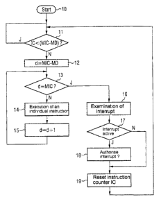
Figure 1 shows the inventive method graphically in the form of a
flow diagram. The following values have to be determined or
initialized before the start of the sequence:
- A counter IC (Instruction Counter), which contains the number
of instructions or machine commands processed by the CPU.
- A number MIC (Maximum Instruction Counter) of instructions,
after which the CPU should change to special operating mode to
process external events.
- A number MD (Maximum Deviation) of instructions, which takes
into account the maximum indeterminacy of the interruption of
the CPU occurring due to the parallel nature of command
execution.
The sequence starts with the current value of the command counter
IC being compared with the difference between the values MIC and MD
(block 11). If the value of the command counter is smaller than
this difference, command processing is continued in standard
operating mode; parallel execution of instructions is possible.
2002P20142WOUS PCT/EP2003/008794
CA 02498596 2005-03-10
9
If the value of the command counter reaches or exceeds the
difference between MIC and MD, a register d is loaded with the
difference between MIC and MD (block 12) and the operation enters a
loop, at the start of which it is asked whether the register d has
reached the value MIC (block 13). In this loop command processing
takes place in single step mode.
As long as the value d does not reach the value MIC, a single
instruction is executed in each passage through the loop (block 14)
and the value d is incremented (block 15) before the loop condition
(block 13) is checked again. This procedure ensures that despite
parallel command processing in standard operation the change to
separate operating state is effected precisely after MIC
instructions.
If the value d reaches the value MIC (block 13), the operation
moves into separate operating mode. Separate operating mode first
verifies whether an interrupt request has been received during
processing of the MIC commands and has been stored in an
intermediate manner for simultaneous processing by all redundant
CPUs (blocks 16/17). If interrupt requests have been received,
these are processed (block 18), whereby said processing is effected
by all redundant CPUs at an identical point in program processing
and all registers, memory contents, etc. are identical. This stage
is omitted, if there are no interrupt requests.
Separate operating mode is terminated and standard operating mode
with parallel instruction processing is resumed after the command
counter IC has been reset (block 19).An interrupt request can then
be processed. The interrupt routine is not processed in separate
operating mode but in standard mode. Only the reading in of the
2002P20142WOUS PCT/EP2003/008794
CA 02498596 2005-03-10
interrupt vector is effected in special operating mode, after which
special mode is left again. Whether or not the interrupt is
processed at this point depends for example on whether interrupts
are permitted at this time. Interrupts are not permitted, if an
5 interrupt is just being processed and/or an "interrupt flag" is
deleted.
The inventive method can be implemented directly as an instruction
sequence, i.e. as software, based on the operation shown. The
10 software thereby ensures that an interrupt is presented at
identical points in the command execution of a plurality of
processors, by programming an instruction counter in the CPU so
that it prompts an exception, e.g. a debug exception, or a high-
priority, non-blockable interrupt, e.g. the non-maskable interrupt
NMI, after the required number MIC of instructions to be processed
minus the "interrupt indeterminacy" MD. For example with an
indeterminacy of MD = 3 instructions and a required number of MIC =
1000 instructions, the counter IC is programmed with 1000-3+1=998.
Depending on the internal grouping of instructions, the CPU is
therefore stopped after IC=998 or IC=999 or IC=1000 instructions.
The software then run reads the instruction counter to determine at
which point the processor actually stopped. This software is
thereby set up so that the execution of its own instructions is
corrected accordingly. If the software determines that the CPU has
stopped for example after 999 instructions, the required 1000th
instruction is executed subsequently by single step operation,
controlled by the exception software. This happens with all
redundant CPUs, so that all CPUs have then been stopped at the
identical point in the code.
Any interruption request present must be presented at this point to
the CPU(s). This can be done as follows:
2002P20142WOUS PCT/EP2003/008794
CA 02498596 2005-03-10
11
- The CPU can read an interrupt controller register, whereupon said
interrupt controller releases a masked interrupt signal. The CPU
identifies an interrupt request from said interrupt signal and
sends an interrupt acknowledge cycle to the interrupt controller.
The interrupt controller then supplies the interrupt vector and
masks the interrupt signal again.
- Alternatively the software can read a register, the value of
which provides information about the nature of the interrupt, i.e.
the interrupt vector. The software itself then initializes the
corresponding interrupt (by software), if interrupts are permitted
in command processing at this time.
The operation can also be achieved in the form of microcode
instructions. In many instances modern CPUs have a wide number of
options for controlling command execution by means of microcode.
These options are frequently used for example to eliminate or
circumvent design errors.
For the purposes of the inventive method the microcode is modified
so that the CPU interrupts standard command execution after the
required number of instructions MIC to be processed minus the
"interrupt indeterminacy" MD and branches into the microcode. The
microcode reads the number of executed instructions IC and
initiates execution by single step so that command execution is
interrupted at the required point MIC.
Any interrupt request present must in turn be presented to the
CPUs) at this point. This can be done in a number of ways:
- An interrupt signal masked by microcode is released by microcode
and if there is an interrupt present, the CPU is branched to the
2002P20142WOUS PCT/EP2003/008794
CA 02498596 2005-03-10
12
corresponding interrupt routine. The interrupt is then masked again
by microcode.
- Alternatively the CPU can be prompted to generate an interrupt
acknowledge cycle and read an interrupt vector. This is then
presented to the CPU by microcode so that after leaving separate
mode the CPU branches to the corresponding interrupt routine.
Implementation can also be effected in the code conversion
software. Some CPUs have a simple but very fast, generally super-
scalar RISC or VLIW processor core. The actual command record, e.g.
IA-32, is transformed by code conversion software to a simple code
and executed by the RISC/VLIW processor. In this case the code
conversion software executes the object of the method, in the same
way as implementation in microcode. Interrupt requests are
presented in the same way as with microcode implementation.
The most efficient implementation of the inventive method is a
hardware implementation, as shown in Figure 2. Here the parallel
command execution is interrupted at the required point minus
indeterminacy by a processor-internal hardware unit S, the
instruction counter status IC is determined and the execution unit
EU is moved on by the processor-internal hardware unit S by single
step ES to the required point in the code. The essential advantage
of this method is the significantly reduced negative influence on
performance.
Figure 2 shows a schematic illustration of an inventive processor
module CPU. Only the components of relevance to this invention are
shown. The CPU comprises one or a plurality of execution units EU,
at least one comparator K, at least one counter IC to count the
instructions executed by the execution unit EU, a controller S and
at least one register element MIR, the content of which can be
2002P20142WOUS PCT/EP2003/008794
CA 02498596 2005-03-10
13
predefined by commands or can be permanently predefined.
Connections from/to an interrupt register are also shown
schematically (Figure 3).
The external events influencing the program sequence are not
supplied directly to the CPU but are first buffered by a suitably
configured hardware unit. The method can be implemented in the CPU
shown in Figure 2, by loading the register MIR with the difference
between the value MIC and the value MD. The comparator K compares
the number of executed operations with this register value and
signals the result of said comparison to the control unit S.
Alternatively the comparator can also send only one event to the
controller, which is generated when the value of the IC has reached
the value of the MIR. If this event has occurred or if equality of
the two registers has been signaled, the controller S asks the
command counter again to read the number of instructions actually
executed. As the indeterminacy has already been taken into account
in the MIR by loading with the value MIC-MD, the controller can
prompt the execution of instructions individually in single step
mode, signaled via the line ES to the execution unit, until the
value of the command counter reaches the predefined value MIC. For
this purpose the controller S is able to increment the command
counter IC, unless the command counter counts the instructions
executed in single step automatically.
The controller S of every redundant CPU generates an interrupt
release signal IF, which is fed to an interrupt module.
Notification of an interrupt request, some of which are stored in
an intermediate manner, is then given to all redundant CPUs via the
interrupt line INT.
Alternatively the controller S generates an interrupt for its own
CPU, whereupon the execution units send an interrupt acknowledge
2002P20142WOUS PCT/EP2003/008794
CA 02498596 2005-03-10
14
cycle to the interrupt module, if interrupts are permitted in the
error processing at this time.
In a further alternative an interrupt signal IF is generated by the
controller S, which is AND-linked as required to the interrupt
signal INT, i.e. the circuit logic should be selected accordingly,
if inverted signals are present or if the interrupt signal is
presented on a plurality of lines. The interrupt release signal can
also be transmitted outside the CPU for example to the interrupt
register. Any interrupts present on the interrupt line INT are
thereby released and normal interrupt management can take place,
e.g. reading of the interrupt vector, execution of the interrupt
routine, etc.
Before interrupt management the cancellation of single step mode
and separate operating mode and the continuation of command
processing in standard mode are signaled to the execution unit and
the command counter is reset via a signal CL. The controller can be
provided directly as hardware or in the form of microcode.
Figure 3 finally shows the interconnection of two CPUs according to
the above description in conjunction with Figure 2. Here the first
processor CPUO and the second processor CPU1 are shown without the
details from Figure 2. The processors respectively exchange
addresses and data via a bus A/D with assigned interrupt modules,
which comprise for example interrupt registers IRO, IR1. The
interrupt modules receive interrupts INTl ... INTn for example from
input/output modules I/O, store corresponding characteristic data
and forward the interrupts INT to the processors.
According to the invention the interrupts are only accepted by the
processors at specific points in the command execution. This is
described in detail in conjunction with Figure 2.
2002P20142WOUS PCT/EP2003/008794
CA 02498596 2005-03-10
The interrupt release signal described in this context can also be
used to signal to the interrupt module assigned to every processor
that interrupt management can be started. The interrupt modules,
which are connected via connections L0, L1, can exchange this
5 information and release interrupt management for their part, for
example by transmitting the interrupt vector to the processors, if
all the processors generate an interrupt release signal.
In one alternative it can prove advantageous not to stop the CPUs
10 at a predefined point MIC in the command execution but at a point
affected by the indeterminacy of commands that can be processed in
parallel and then to move the processors that are behind on by
single step to the point in command processing at which the
processor that has progressed furthest in command processing has
15 stopped. This requires communication between the processors. This
can be effected for example in such a way that every processor
writes the point at which it stopped itself in a hardware register
and then reads it back. The register waits until all the processors
have written in their value and supplies the highest value as read
data. If necessary all the processors then align their command
execution status by single step. The interrupt request is then
presented to the processors as described above.
CPUs which have SMT (Simultaneous Multi Threading) capabilities
have to have a separate controller for every virtual CPU or every
thread.
The CPU also comprises the comparator K, which compares the number
of executed commands, i.e. the counter IC, with the register MIR
and in the event of equality generates an interrupt request for
example, which interrupts command execution after the number of
2002P20142WOUS PCT/EP2003/008794
CA 02498596 2005-03-10
16
instructions predefined by the register MIR and switches the CPU to
a different operating mode. In this operating mode for example an
appropriate microcode is executed or a branch is made to an
interrupt service routine or the reaching of said synchronization
point is signaled by hardware signals. In this operating mode the
external events are presented to the redundant CPUs in such a way
that after leaving said operating mode all the CPUs can evaluate
said events in the same way and the same commands are therefore
executed as a result.
For example after reaching the number of machine instructions
predefined by the register MIR, the CPU branches into an interrupt
service routine, in which the status of interrupt signals kept
remote from the CPU by the described hardware is requested so that
a redundant CPU, which may make said request at a slightly later
time, receives identical information.
On leaving separate operating mode the counter IC is reset. There
is then a return to the program point, at which the interrupt took
place due to reaching the counter value IC predefined by the
register MIR. The CPU will then execute the number of machine
instructions predefined by the register MIR again and when the
counter IC reaches the register value MIR it will change mode,
thereby allowing the acceptance of external events.
The CPU registers MIR are advantageously configured so that they
can be written by software or microcode, to ensure that interrupt
management takes place at appropriate intervals for different areas
of use, by determining the time windows for interrupt management
according to the number of instructions to be executed.