Note: Descriptions are shown in the official language in which they were submitted.
CA 02498916 2005-03-14
WO 2004/025561 PCT/US2003/028887
Chemical Synthesis Using
Diffraction Grating-Based Encoded Optical Elements
Cross References to Related Applications
This application claims the benefit of US Provisional Patent Applications,
Serial No. 60/410,541 (CiDRA Docket No. CC-543), filed Sept. 12, 2002, and is
a
continuation-in-part of US Patent Applications, Serial No. (CiDRA Docket No.
CC-
0648), filed Aug. 20, 2003, and is a continuation-in-part of US Patent
Application,
Serial No. (CiDRA Docket No. CC-0649), filed Aug. 20, 2003, each of which are
incorporated herein by reference in their entirety.
US Patent Application Serial No. (CiDRA Docket No. CC-0648A) and
Application Serial No. (CiDItA Docket No. CC-0650), filed contemporaneously
herewith, contains subject matter related to that disclosed herein, which is
incorporated by reference in its entirety.
Technical Field
This invention relates to chemical synthesis, and more particularly to
chemical
synthesis that use optically encoded beads, micro-particles, or elements.
Background Art
A common form of chemical synthesis in combinatorial chemistry is known as
"solid phase" chemical synthesis. This synthesis technique uses encoded beads
or
particles as a solid support for the synthesis of chemicals and or chemical
libraries
Existing technologies, such as bar codes, electronic microchips/transponders,
radio-frequency identification (RFID), and fluorescence and other optical
techniques,
are often inadequate. For example, existing technologies may be too large for
certain
applications, may not provide enough different codes (i.e., limited
multiplexing
CA 02498916 2005-03-14
WO 2004/025561 PCT/US2003/028887
capability), or cannot withstand harsh temperature, chemical, nuclear and/or
electromagnetic environments, or may otherwise be not well suited for certain
types
of chemical synthesis or true combinatorial chemistry.
Therefore, it would be desirable to obtain a coding element or platform that
provides the capability of providing many codes (e.g., greater than 1 million
codes),
that can be made very small, that can withstand harsh environments, and/or can
enable "true" combinatorial chemistry.
Summary of the Invention
Objects of the present invention include provision of an optical
identification
element or platform that allows for a large number of distinct codes, can be
made very
small, and/or can withstand harsh environments.
According to the present invention, an optical identification element attached
to a chemical, comprises an optical substrate; at least a portion of the
substrate having
at least one diffraction grating disposed therein, the grating having at least
one
refractive index pitch superimposed at a common location; the grating
providing an
output optical signal when illuminated by an incident light signal; the
optical output
signal being indicative of a code in the substrate; and the chemical being
attached to
the substrate.
The present invention provides an encoded optical element platform for
performing large numbers of combinatorial chemistry tasks/experiments.
Also, the elements may be very small "microbeads" (or microelements or
microparticles or encoded particles) for synthesis that requires small
substrates (about
1-1000 microns), or larger "macroelements" for synthesis that allows for
larger
substrates or beads (e.g., 1-1000mm or much larger). The elements may also be
referred to as encoded particles or encoded threads. Also, the element may be
embedded within or part of a larger substrate or object. A common synthesis
use will
be as microbeads. Also, chemicals can be synthesized on microbeads located in
a
glass column reaction vessel.
-2-
CA 02498916 2005-03-14
WO 2004/025561 PCT/US2003/028887
The beads may be chemically coated before or after synthesis, to either
enhance chemical synthesis or help preserve it after synthesis is complete.
The invention may be used with any known combinatorial chemistry or
biochemistry synthesis process, and are especially adaptable to synthesis
processes
having solid phase immobilization. The invention may be used in many areas
such as
drug discovery, biology, proteomics, combinatorial chemistry, assays or
multiplexed
experiments. Any type of chemical, or molecule chain that can be synthesized
on a
glass or other solid support bead may be synthesized using the present
invention as
the solid support. For example, genes, DNA, cDNA, RNA, proteins, particles,
biological particles, cells, molecules, atoms, nucleotides, oligomers,
peptides, antigen,
antibodies, ligands, receptors, hydrocarbons, polymers, radioactive or non-
radioactive
particles.
The elements also allow for quality control of the synthesized chemical to be
easily tested, providing a higher level of quality chemicals.
1 S The foregoing and other objects, features and advantages of the present
invention will become more apparent in light of the following detailed
description of
exemplary embodiments thereof.
Brief Description of the Drawings
Fig. 1 is a side view of an optical identification element, in accordance with
the present invention.
Fig. 2 is a top level optical schematic for reading a code in an optical
identification element, in accordance with the present invention.
Fig. 3 is a flow chart for a chemical split and pool chemical synthesis
process,
in accordance with the present invention.
Fig. 4 is a diagram of a chemical split and pool synthesis apparatus, in
accordance with the present invention.
Fig. 5 is an optical schematic for reading a code in an optical identification
element, in accordance with the present invention.
-3-
CA 02498916 2005-03-14
WO 2004/025561 PCT/US2003/028887
Fig. 6 is an image of a code on a CCD camera from an optical identification
element, in accordance with the present invention.
Fig. 7 is a graph showing an digital representation of bits in a code in an
optical identification element, in accordance with the present invention.
Fig. 8 illustrations (a)-(c) show images of digital codes on a CCD camera, in
accordance with the present invention.
Fig. 9 illustrations (a)-(d) show graphs of different refractive index pitches
and
a summation graph, in accordance with the present invention.
Fig. 10 is an alternative optical schematic for reading a code in an optical
identification element, in accordance with the present invention.
Fig. 11 illustrations (a)-(b) are graphs of reflection and transmission
wavelength spectrum for an optical identification element, in accordance with
the
present invention.
Figs. 12-13 are side views of a thin grating for an optical identification
1 S element, in accordance with the present invention.
Fig. 14 is a perspective view showing azimuthal multiplexing of a thin grating
for an optical identification element, in accordance with the present
invention.
Fig. 1 S is side view of a blazed grating for an optical identification
element, in
accordance with the present invention.
Fig. 16 is a graph of a plurality of states for each bit in a code for an
optical
identification element, in accordance with the present invention.
Fig. 17 is a side view of an optical identification element where light is
incident on an end face, in accordance with the present invention.
Figs. 18-19 are side views of an optical identification element where light is
incident on an end face, in accordance with the present invention.
Figs. 20, illustrations (a)-(c) are side views of an optical identification
element
having a blazed grating, in accordance with the present invention.
Fig. 21 is a side view of an optical identification element having a coating,
in
accordance with the present invention.
-4-
CA 02498916 2005-03-14
WO 2004/025561 PCT/US2003/028887
Fig. 22 is a side view of whole and partitioned optical identification
element,
in accordance with the present invention.
Fig. 23 is a side view of an optical identification element having a grating
across an entire dimension, in accordance with the present invention.
Fig. 24, illustrations (a)-(c), are perspective views of alternative
embodiments
for an optical identification element, in accordance with the present
invention.
Fig. 25, illustrations (a)-(b), are perspective views of an optical
identification
element having multiple grating locations, in accordance with the present
invention.
Fig. 26, is a perspective view of an alternative embodiment for an optical
identification element, in accordance with the present invention.
Fig. 27 is a view an optical identification element having a plurality of
gratings located rotationally around the optical identification element, in
accordance
with the present invention.
Fig. 28 illustrations (a)-(e) show various geometries of an optical
identification element that may have holes therein, in accordance with the
present
invention.
Fig. 29 illustrations (a)-(c) show various geometries of an optical
identification element that may have teeth thereon, in accordance with the
present
invention.
Fig. 30 illustrations (a)-(c) show various geometries of an optical
identification element, in accordance with the present invention.
Fig. 31 is a side view an optical identification element having a reflective
coating thereon, in accordance with the present invention.
Fig. 32 illustrations (a)-(b) are side views of an optical identification
element
polarized along an electric or magnetic field, in accordance with the present
invention.
Best Mode for Carrying Out the Invention
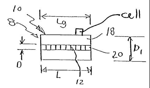
Referring to Fig. 1, a diffraction grating-based optical identification
element 8
(or encoded element or coded element) comprises a known optical substrate 10,
-5-
CA 02498916 2005-03-14
WO 2004/025561 PCT/US2003/028887
having an optical diffraction grating 12 disposed (or written, impressed,
embedded,
imprinted, etched, grown, deposited or otherwise formed) in the volume of or
on a
surface of a substrate 10. The grating 12 is a periodic or aperiodic variation
in the
effective refractive index and/or effective optical absorption of at least a
portion of the
substrate 10.
The optical identification element 8 described herein is the same as that
described in Copending Patent Application Serial No. (CiDRA Docket No. CC-
0648A), and in Copending Patent Application Serial No. (CiDRA Docket No. CC-
0649A), both filed contemporaneously herewith, which are both incorporated
herein
by reference in their entirety.
In particular, the substrate 10 has an inner region 20 where the grating 12 is
located. The inner region 20 may be photosensitive to allow the writing or
impressing
of the grating 12. The substrate 10 has an outer region 18, which does not
have the
grating 12 therein.
The grating 12 is a combination of one or more individual spatial periodic
sinusoidal variations (or components) in the refractive index that are
collocated at
substantially the same location on the substrate 10 along the length of the
grating
region 20, each having a spatial period (or pitch) A. The resultant
combination of
these individual pitches is the grating 12, comprising spatial periods (A1-An)
each
representing a bit in the code. Thus, the grating 12 represents a unique
optically
readable code, made up of bits, where a bit corresponds to a unique pitch A
within the
grating 12. Accordingly, for a digital binary (0-1) code, the code is
determined by
which spatial periods (A1-An) exist (or do not exist) in a given composite
grating 12.
The code or bits may also be determined by additional parameters (or
additional
degrees of multiplexing), and other numerical bases for the code may be used,
as
discussed herein and/or in the aforementioned patent application.
The grating 12 may also be referred to herein as a composite or collocated
grating. Also, the grating 12 may be referred to as a "hologram", as the
grating 12
-6-
CA 02498916 2005-03-14
WO 2004/025561 PCT/US2003/028887
transforms, translates, or filters an input optical signal to a predetermined
desired
optical output pattern or signal.
The substrate 10 has an outer diameter D1 and comprises silica glass (SiOZ)
having the appropriate chemical composition to allow the grating 12 to be
disposed
therein or thereon. Other materials for the optical substrate 10 may be used
if desired.
For example, the substrate 10 may be made of any glass, e.g., silica,
phosphate glass,
borosilicate glass, or other glasses, or made of glass and plastic, or solely
plastic. For
high temperature or harsh chemical applications, the optical substrate 10 made
of a
glass material is desirable. If a flexible substrate is needed, plastic,
rubber or
polymer-based substrate may be used. The optical substrate 10 may be any
material
capable of having the grating 12 disposed in the grating region 20 and that
allows
light to pass through it to allow the code to be optically read.
The optical substrate 10 with the grating 12 has a length L and an outer
diameter D1, and the inner region 20 diameter D. The length L can range from
very
small "microbeads" (or microelements, micro-particles, or encoded particles),
about
1-1000 microns or smaller, to larger "macrobeads" or "macroelements" for
larger
applications (about 1.0 - 1000 mm or greater). In addition, the outer
dimension D1
can range from small (less than 1000 microns) to large (1.0 - 1000 mm and
greater).
Other dimensions and lengths for the substrate 10 and the grating 12 may be
used.
The grating 12 may have a length Lg of about the length L of the substrate 10.
Alternatively, the length Lg of the grating 12 may be shorter than the total
length L of
the substrate 10.
The outer region 18 is made of pure silica (SiOz) and has a refractive index
n2
of about 1.458 (at a wavelength of about 1553 nm), and the inner grating
region 20 of
the substrate 10 has dopants, such as germanium and/or boron, to provide a
refractive
index nl of about 1.453, which is less than that of outer region 18 by about
0.005.
Other indices of refraction nl,n2 for the grating region 20 and the outer
region 18,
respectively, may be used, if desired, provided the grating 12 can be
impressed in the
desired grating region 20. For example, the grating region 20 may have an
index of
CA 02498916 2005-03-14
WO 2004/025561 PCT/US2003/028887
refraction that is larger than that of the outer region 18 or grating region
20 may have
the same index of refraction as the outer region 18 if desired.
Referring to Fig. 2, an incident light 24 of a wavelength ~,, e.g., 532 nm
from a
known frequency doubled Nd:YAG laser or 632nm from a known Helium-Neon laser,
is incident on the grating 12 in the substrate 10. Any other input wavelength
~, can be
used if desired provided 7~ is within the optical transmission range of the
substrate
(discussed more herein and/or in the aforementioned patent application). A
portion of
the input light 24 passes straight through the grating 12, as indicated by a
line 25. The
remainder of the input light 24 is reflected by the grating 12, as indicated
by a line 27
and provided to a detector 29. The output light 27 may be a plurality of
beams, each
having the same wavelength ~, as the input wavelength 7~ and each having a
different
output angle indicative of the pitches (Al-An) existing in the grating 12.
Alternatively, the input light 24 may be a plurality of wavelengths and the
output light 27 may have a plurality of wavelengths indicative of the pitches
(A1-An)
existing in the grating 12. Alternatively, the output light may be a
combination of
wavelengths and output angles. The above techniques are discussed in more
detail
herein and/or in the aforementioned patent application.
The detector 29 has the necessary optics, electronics, software and/or
firmware
to perform the functions described herein. In particular, the detector reads
the optical
signal 27 diffracted or reflected from the grating 12 and determines the code
based on
the pitches present or the optical pattern, as discussed more herein or in the
aforementioned patent application. An output signal indicative of the code is
provided
on a line 31.
Referring to Fig. 3, the optical elements described herein may be used to
synthesize chemicals in a known split and pool synthesis technique. In
particular, a
known split and pool bead based synthesis process 801, may be performed
starting
with a step 800 where a predetermined number M of compounds or chemicals are
provided each in a separate bin or container and at step 802 where a
predetermined
number X of microbeads 8 are provided each having it own unique code. Steps
800,
_g_
CA 02498916 2005-03-14
WO 2004/025561 PCT/US2003/028887
802 are material preparation steps and can be done in either order. After the
materials
are prepared, a step 803 combines or pools all the beads together. Then, a
step 804
determines the code for each microbead 8. This step can be skipped on the
first time
through the process if it is desired to randomly split up the beads into
groups, i.e., to
not split the groups up by code on bead during the first run. Next a step 806
sorts the
beads based on its code and deposits the bead into the appropriate bin for the
chemical
to be added to the bead.
Next, a step 808 tests to see if the chemical synthesis is complete for each
bead. If not the process goes back to step 803 where the remaining beads are
recombines or re-pools and the process starts again. The loop 814 repeats a
predetermined number of times N, where each time through the loop 814 another
chemical is added to each of the beads. If certain beads are to have fewer
chemicals
than others, then certain beads will drop out of the process before others.
When the
step 808 concludes that one or more beads have completed their synthesis
process, a
step 812 logs the completion of that bead and the remainder of the beads
continue
until all desired chemicals have synthesized on the beads.
For example, for M=4 compounds and N=10 chemicals to add to each bead,
the total number of different codes needed would be 1,048,576 or MN and if
there will
be only one bead with each desired chemical (i.e., no redundancy), then the
number of
beads X would also be MN = 1,048,576.
Referring to Fig. 4, an automated synthesis machine is shown for synthesizing
a chemical having four different possible compounds or cells or molecules
(e.g.,
GCAT for a DNA synthesis), where a main bin 830 receives or pools all the
beads 8
and provides the beads 8 to a sorting machine 832 , which performs the sorting
step
806 in the loop 814. In addition the machine 832 deposits the beads in the
proper bins
834,836, 838,840, having the bases G,C,A,T, respectively. Any other four
chemicals
can be used if desired. Once the specific base has been attached to a bead it
is dropped
or placed in a device which transports the beads back into the main bin 830
for
-9-
CA 02498916 2005-03-14
WO 2004/025561 PCT/US2003/028887
resorting by the machine 832. When synthesis has been completed on a given
bead
the machine deposits the completed bead in a done bin 844.
If it is desired to produce multiple of the same chemical on separate beads
this
can be done by having multiple beads with the same code, or presetting certain
groups
of codes to have the same chemical composition. In that case, each of these
beads
may go to the same bins in the same order as a group.
The present invention may be used with any known combinatorial chemistry,
chemical synthesis process, or synthesizing labeled combinatorial chemistry
libraries,
and are especially adaptable to solid phase synthesis, for example: US
Patents,
6,417,010, "Methods and Apparatus for Synthesizing Labeled Combinatorial
Chemistry Labraries", 6,558,904 entitled "Method for producing structured,
self
organized molecular monolayers of individual molecular species, in particular
substance libraries"; 6,541,276 entitled "Methods for solid-phase synthesis of
'
hydroxylamine compounds and derivatives and combinatorial libraries thereof';
6,541,211 "Apparatus and method for synthesizing combinational libraries";
6,528,324 entitled " Apparatus for pre-determined mass sorting of positional-
encoded
solid phase synthesis supports"; 6,506,558 entitled "Very large scale
immobilized
polymer synthesis"; 6,495,539 entitled "B-lactam-like chaperone inhibitors";
6,468,740 entitled "Cyclic and substituted immobilized molecular synthesis";
6,417,010 entitled "Methods and apparatus for synthesizing labeled
combinatorial
chemistry libraries; 6,410,643 entitled "Solid phase synthesis method and
reagent";
6,410,342 entitled "Method and apparatus for controlled photoelution";
6,387,636
entitled "Method of shielding biosynthesis reactions from the ambient
environment on
an array"; 6,372,885 entitled "Solid-phase technology for the preparation of
amides"; 6,368,874 entitled "Methods for hard-tagging an encoded synthetic
library"; 6,362,009 entitled "Solid phase synthesis of heterocycles";
6,346,423
entitled "Methods and compositions for producing biopolymeric arrays";
6,329,210
entitled "Method and apparatus for high volume polymer synthesis"; 6,294,694
entitled "Matrix metalloproteinase inhibitors and method of using same";
6,274,385
- 10-
CA 02498916 2005-03-14
WO 2004/025561 PCT/US2003/028887
entitled "Attached tags for use in combinatorial chemistry synthesis";
6,265,228
entitled "Process for preparing combinatorial amide alcohol libraries";
6,251,595
entitled "Methods and devices for carrying out chemical reactions"; 6,127,190
entitled "Method for producing combinatorial libraries having a predetermined
S frequency of each species of test compound"; 5,929,208 entitled "Methods for
electronic synthesis of polymers"; 5,886,186 entitled "Synthesis of
substituted N-
heteroaromatic compounds and methods of use thereof'; 5,885,837 entitled "Very
large scale immobilized polymer synthesis using mechanically directed flow
paths";
5,859,191 entitled "Method for the site-specific modification of peptide alpha
amines"; 5,763,263 entitled "Method and apparatus for producing-position
addressable combinatorial libraries"; 5,712,171 entitled "Method of generating
a
plurality of chemical compounds in a spatially arranged array"; 5,690,894
entitled
"High density array fabrication and readout method for a fiber optic
biosensor";
5,545,568 entitled "Solid phase and combinatorial synthesis of compounds on a
solid
support"; 5,545,531 entitled "Methods for making a device for concurrently
processing multiple biological chip assays"; 5,539,083 entitled "Peptide
nucleic acid
combinatorial libraries and improved methods of synthesis"; 5,384,261 entitled
"Very large scale immobilized polymer synthesis using mechanically directed
flow
paths"; 5,288,514 entitled "Solid phase and combinatorial synthesis of
benzodiazepine compounds on a solid support"; 5,264,563 entitled "Process for
synthesizing oligonucleotides with random codons"; 5,010,175 entitled "General
method for producing and selecting peptides with specific properties";
6,465,192
entitled "Compounds and methods for the inhibition of protein-protein
interactions";
6,440,669 entitled "Methods for applying small volumes of reagents"; 6,406,844
2S entitled "Very large scale immobilized polymer synthesis"; 6,329,010
entitled
"Method and apparatus for high volume polymer synthesis"; 6,316,623 entitled
"Ethylenediamine compound libraries"; 5,780,241 entitled "Complex chemical
libraries"; 5,712,171 entitled "Method of generating a plurality of chemical
compounds in a spatially arranged array"; 5,593,853 entitled "Generation and
-11-
CA 02498916 2005-03-14
WO 2004/025561 PCT/US2003/028887
screening of synthetic drug libraries"; 6,569,631 entitled "Microplate thermal
shift
assay for ligand development using 5-(4"dimethylaminophenyl)- 2-(4'-
phenyl)oxazole derivative fluorescent dyes"; 6,503,759 entitled "Complex
combinatorial chemical libraries encoded with tags"; 6,492,125 entitled
"Method to
assess library X library interactions"; 6,457,807 entitled "Mass-based
encoding and
qualitative analysis of combinatorial libraries"; 6,455,263 entitled "Small
molecule
library screening using FACS"; 6,096,496 entitled "Supports incorporating
vertical
cavity emitting lasers and tracking apparatus for use in combinatorial
synthesis";
5,770,455 entitled "Methods and apparatus for synthesizing labeled
combiatorial
chemistrylibraries"; 5,751,629 entitled "Remotely programmable matrices with
memories"; 6,537,504 "Method and apparatus for concurrent and sequential multi-
step reactions for producing a plurality of different chemical compounds";
6,468,806
"Potential masking systems and methods for combinatorial library synthesis";
6,429,027 "Composite arrays utilizing microspheres"; 6,420,169 "Apparatus for
forming polynucleotides or polypeptides"; 6,448,443 "Synthesis of
combinatorial
libraries of compounds reminiscent of natural products"; 5,840,485
"Topologically
segregated, encoded solid phase libraries".
Referring to Fig. 5, The reflected light 27, comprises a plurality of beams 26-
36 that pass through a lens 37, which provides focused light beams 46-56,
respectively, which are imaged onto a CCD camera 60. The lens 37 and the
camera
60, and any other necessary electronics or optics for performing the functions
described herein, make up the reader 29. Instead of or in addition to the lens
37, other
imaging optics may be used to provide the desired characteristics of the
optical
image/signal onto the camera 60 (e.g., spots, lines, circles, ovals, etc.),
depending on
the shape of the substrate 10 and input optical signals. Also, instead of a
CCD camera
other devices may be used to read/capture the output light.
Referring to Fig. 6, the image on the CCD camera 60 is a series of illuminated
stripes indicating ones and zeros of a digital pattern or code of the grating
12 in the
-12-
CA 02498916 2005-03-14
WO 2004/025561 PCT/US2003/028887
element 8. Referring to Fig. 7, lines 68 on a graph 70 are indicative of a
digitized
version of the image of Fig. 6 as indicated in spatial periods (A1-An).
Each of the individual spatial periods (A1-An) in the grating 12 is slightly
different, thus producing an array of N unique diffraction conditions (or
diffraction
S angles) discussed more hereinafter. When the element 8 is illuminated from
the side,
in the region of the grating 12, at an appropriate input angle, e.g., about 30
degrees,
with a single input wavelength ~, (monochromatic) source, the diffracted (or
reflected)
beams 26-36 are generated. Other input angles 8i may be used if desired,
depending
on various design parameters as discussed herein and/or in the aforementioned
patent
application, and provided that a known diffraction equation (Eq. 1 below) is
satisfied:
sin(B; ) + sin(eo ) = m~. / nA Eq. 1
where Eq. 1 is diffraction (or reflection or scatter) relationship between
input
wavelength 7~, input incident angle 8i, output incident angle 00, and the
spatial period
A of the grating 12. Further, m is the "order" of the reflection being
observed, and n is
the refractive index of the substrate 10. The value of m=1 or first order
reflection is
acceptable for illustrative purposes. Eq. 1 applies to light incident on outer
surfaces of
the substrate 10 which are parallel to the longitudinal axis of the grating
(or the kB
vector). Because the angles Ai,Oo are defined outside the substrate 10 and
because the
effective refractive index of the substrate 10 is substantially a common
value, the
value of n in Eq. 1 cancels out of this equation.
Thus, for a given input wavelength ~,, grating spacing A, and incident angle
of
the input light 0i, the angle 80 of the reflected output light may be
determined.
Solving Eq. 1 for 0o and plugging in m=l, gives:
80 = sin-~(~1~1- sin(6 i)) Eq. 2
For example, for an input wavelength ~, = 532 nm, a grating spacing A= 0.532
microns (or 532 nm), and an input angle of incidence 0i =30 degrees, the
output angle
of reflection will be 00 = 30 degrees. Alternatively, for an input wavelength
~. = 632
nm, a grating spacing A = 0.532 microns (or 532 nm), and an input angle Oi of
30
-13-
CA 02498916 2005-03-14
WO 2004/025561 PCT/US2003/028887
degrees, the output angle of reflection Oo will be at 43.47 degrees, or for an
input
angle 8i = 37 degrees, the output angle of reflection will be 00 = 37 degrees.
Any
input angle that satisfies the design requirements discussed herein and/or in
the
aforementioned patent application may be used.
In addition, to have sufficient optical output power and signal to noise
ratio,
the output light 27 should fall within an acceptable portion of the Bragg
envelope (or
normalized reflection efficiency envelope) curve 200, as indicated by points
204,206,
also defined as a Bragg envelope angle OB, as also discussed herein and/or in
the
aforementioned patent application. The curve 200 may be defined as:
I (ki, ko) ~ ~KD~Z sin cz (ki -~ o)D Eq. 3
where K = 2~8n/7~, where, 8n is the local refractive index modulation
amplitude of the
grating and ~, is the input wavelength, sinc(x) = sin(x)/x, and the vectors k;
_
2~cos(0;)/~, and ko= 2~cos (60)/7 are the projections of the incident light
and the
output (or reflected) light, respectively, onto the line 203 normal to the
axial direction
of the grating 12 (or the grating vector k,~), D is the thickness or depth of
the grating
12 as measured along the line 203 (normal to the axial direction of the
grating 12).
Other substrate shapes than a cylinder may be used and will exhibit a similar
peaked
characteristic of the Bragg envelope. We have found that a value for 8n of
about 10~
in the grating region of the substrate is acceptable; however, other values
may be used
if desired.
Rewriting Eq. 3 gives the reflection efficiency profile of the Bragg envelope
as:
I(ki,ko)~~2~'Sn~D~z~Sin(x)~z Eq.4
x
where: x =(ki-ko)Dl2 = (~cDl~,) *(cos 8 i - cos 8 0)
Thus, when the input angle 8i is equal to the output (or reflected) angle Oo
(i.e., Oi = 00), the reflection efficiency I (Eqs. 3 & 4) is maximized, which
is at the
- 14-
CA 02498916 2005-03-14
WO 2004/025561 PCT/US2003/028887
center or peak of the Bragg envelope. When 8i = 80, the input light angle is
referred
to as the Bragg angle as is known. The efficiency decreases for other input
and output
angles (i.e., 8i ~ 0°), as defined by Eqs. 3 & 4. Thus, for maximum
reflection
efficiency and thus output light power, for a given grating pitch A and input
wavelength, the angle 0i of the input light 24 should be set so that the angle
80 of the
reflected output light equals the input angle Ai.
Also, as the thickness or diameter D of the grating decreases, the width of
the
sin(x)/x function (and thus the width of the Bragg envelope) increases and,
the
coefficient to or amplitude of the since (or (sin(x)/x) z function (and thus
the efficiency
level across the Bragg envelope) also increases, and vice versa. Further, as
the
wavelength ~, increases, the half width of the Bragg envelope as well as the
efficiency
level across the Bragg envelope both decrease. Thus, there is a trade-off
between the
brightness of an individual bit and the number of bits available under the
Bragg
envelope. Ideally, 8n should be made as large as possible to maximize the
brightness,
which allows D to be made smaller.
From Eq. 3 and 4, the half angle of the Bragg envelope AB is defined as:
BB = ~ Eq. S
~D sin(0; )
where r~ is a reflection efficiency factor which is the value for x in the
sincz(x)
function where the value of sincZ(x) has decreased to a predetermined value
from the
maximum amplitude as indicated by points 204,206 on the curve 200.
We have found that the reflection efficiency is acceptable when rl < 1.39.
This
value for r) corresponds to when the amplitude of the reflected beam (i.e.,
from the
sincz(x) function of Eqs. 3 & 4) has decayed to about 50% of its peak value.
In
particular, when x = 1.39 = r~, sincz(x) = 0.5. However, other values for
efficiency
thresholds or factor in the Bragg envelope may be used if desired.
The beams 26-36 are imaged onto the CCD camera 60 to produce the pattern
of light and dark regions 120-132 representing a digital (or binary) code,
where light
-15-
CA 02498916 2005-03-14
WO 2004/025561 PCT/US2003/028887
= 1 and dark = 0 (or vice versa). The digital code may be generated by
selectively
creating individual index variations (or individual gratings) with the desired
spatial
periods A1-An. Other illumination, readout techniques, types of gratings,
geometries,
materials, etc. may be used as discussed in the aforementioned patent
application.
Referring to Fig.B, illustrations (a)-(c), for the grating 12 in a cylindrical
substrate 10 having a sample spectral 17 bit code (i.e., 17 different pitches
Al-A17),
the corresponding image on the CCD (Charge Coupled Device) camera 60 is shown
for a digital pattern of 7 bits turned on (10110010001001001); 9 bits turned
on of
(11000101010100111); all 17 bits turned on of (11111111111111111).
For the images in Fig. 8, the length of the substrate 10 was 450 microns, the
outer diameter D1 was 65 microns, the inner diameter D was 14 microns, 8n for
the
grating 12 was about 10~, nl in portion 20 was about 1.458 (at a wavelength of
about
1550 nm), n2 in portion 18 was about 1.453, the average pitch spacing A for
the
grating 12 was about 0.542 microns, and the spacing between pitches 4A was
about
0.36 % of the adjacent pitches A.
Referring to Fig. 9, illustration (a), the pitch A of an individual grating is
the
axial spatial period of the sinusoidal variation in the refractive index nl in
the region
of the substrate 10 along the axial length of the grating 12 as indicated by a
curve
90 on a graph 91. Referring to Fig. 9, illustration (b), a sample composite
grating 12
20 comprises three individual gratings that are co-located on the substrate
10, each
individual grating having slightly different pitches, A1, A2, A3,
respectively, and the
difference (or spacing) ~A between each pitch A being about 3.0 % of the
period of
an adjacent pitch A as indicated by a series of curves 92 on a graph 94.
Referring to
Fig. 9, illustration (c), three individual gratings, each having slightly
different pitches,
Al, A2, X13, respectively, are shown, the difference DA between each pitch A
being
about 0.3% of the pitch A of the adjacent pitch as shown by a series of curves
95 on a
graph 97. The individual gratings in Fig. 9, illustrations (b) and (c) are
shown to all
start at 0 for illustration purposes; however, it should be understood that,
the separate
-16-
CA 02498916 2005-03-14
WO 2004/025561 PCT/US2003/028887
gratings need not all start in phase with each other. Referring to Fig. 9,
illustration (d),
the overlapping of the individual sinusoidal refractive index variation
pitches A1-An
in the grating region 20 of the substrate 10, produces a combined resultant
refractive
index variation in the composite grating 12 shown as a curve 96 on a graph 98
representing the combination of the three pitches shown in Fig. 9,
illustration (b).
Accordingly, the resultant refractive index variation in the grating region 20
of the
substrate 10 may not be sinusoidal and is a combination of the individual
pitches A
(or index variation).
The maximum number of resolvable bits N, which is equal to the number of
different grating pitches A (and hence the number of codes), that can be
accurately
read (or resolved) using side-illumination and side-reading of the grating 12
in the
substrate 10, is determined by numerous factors, including: the beam width w
incident
on the substrate (and the corresponding substrate length L and grating length
Lg), the
thickness or diameter D of the grating 12, the wavelength ~, of incident
light, the beam
divergence angle OR, and the width of the Bragg envelope Aa (discussed more in
the
aforementioned patent application), and may be determined by the equation:
N - ~~L Eq. 6
2D sin( Bi )
Referring to Fig. 10, instead of having the input light 24 at a single
wavelength
7~ (monochromatic) and reading the bits by the angle Ao of the output light,
the bits (or
grating pitches A) may be read/detected by providing a plurality of
wavelengths and
reading the wavelength spectrum of the reflected output light signal. In this
case, there
would be one bit per wavelength, and thus, the code is contained in the
wavelength
information of the reflected output signal.
In this case, each bit (or A) is defined by whether its corresponding
wavelength falls within the Bragg envelope, not by its angular position within
the
Bragg envelope 200. As a result, it is not limited by the number of angles
that can fit
in the Bragg envelope 200 for a given composite grating 12, as in the
embodiment
discussed hereinbefore. Thus, using multiple wavelengths, the only limitation
in the
-17-
CA 02498916 2005-03-14
WO 2004/025561 PCT/US2003/028887
number of bits N is the maximum number of grating pitches A that can be
superimposed and optically distinguished in wavelength space for the output
beam.
Referring to Figs. 10 and 11, illustration (a), the reflection wavelength
spectrum (~,1-~,n) of the reflected output beam 310 will exhibit a series of
reflection
peaks 695, each appearing at the same output Bragg angle Bo. Each wavelength
peak
695 (~,1-7~n) corresponds to an associated spatial period (A1-An), which make
up the
grating 12.
One way to measure the bits in wavelength space is to have the input light
angle 8i equal to the output light angle Oo, which is kept at a constant
value, and to
provide an input wavelength 7~ that satisfies the diffraction condition (Eq.
1) for each
grating pitch A. This will maximize the optical power of the output signal for
each
pitch A detected in the grating 12.
Referring to 11, illustration (b), the transmission wavelength spectrum of the
transmitted output beam 330 (which is transmitted straight through the grating
12)
I 5 will exhibit a series of notches (or dark spots) 696. Alternatively,
instead of detecting
the reflected output light 310, the transmitted light 330 may be detected at
the
detector/reader 308. It should be understood that the optical signal levels
for the
reflection peaks 695 and transmission notches 696 will depend on the
"strength" of
the grating 12, i.e., the magnitude of the index variation n in the grating
12.
1n Fig. 10, the bits may be detected by continuously scanning the input
wavelength. A known optical source 300 provides the input light signal 24 of a
coherent scanned wavelength input light shown as a graph 304. The source 300
provides a sync signal on a line 306 to a known reader 308. The sync signal
may be a
timed pulse or a voltage ramped signal, which is indicative of the wavelength
being
provided as the input light 24 to the substrate 10 at any given time. The
reader 308
may be a photodiode, CCD camera, or other optical detection device that
detects
when an optical signal is present and provides an output signal on a line 309
indicative of the code in the substrate 10 or of the wavelengths present in
the output
light, which is directly related to the code, as discussed herein. The grating
12 reflects
-18-
CA 02498916 2005-03-14
WO 2004/025561 PCT/US2003/028887
the input light 24 and provides an output light signal 310 to the reader 308.
The
wavelength of the input signal is set such that the reflected output light 310
will be
substantially in the center 314 of the Bragg envelope 200 for the individual
grating
pitch (or bit) being read.
Alternatively, the source 300 may provide a continuous broadband wavelength
input signal such as that shown as a graph 316. In that case, the reflected
output beam
310 signal is provided to a narrow band scanning filter 318 which scans across
the
desired range of wavelengths and provides a filtered output optical signal 320
to the
reader 308. The filter 318 provides a sync signal on a line 322 to the reader,
which is
indicative of which wavelengths are being provided on the output signal 320 to
the
reader and may be similar to the sync signal discussed hereinbefore on the
line 306
from the source 300. In this case, the source 300 does not need to provide a
sync
signal because the input optical signal 24 is continuous. Alternatively,
instead of
having the scanning filter being located in the path of the output beam 310,
the
scanning filter may be located in the path of the input beam 24 as indicated
by the
dashed box 324, which provides the sync signal on a line 323.
Alternatively, instead of the scanning filters 318,324, the reader 308 may be
a
known optical spectrometer (such as a known spectrum analyzer), capable of
measuring the wavelength of the output light.
The desired values for the input wavelengths ~, (or wavelength range) for the
input signal 24 from the source 300 may be determined from the Bragg condition
of
Eq. 1, for a given grating spacing A and equal angles for the input light Ai
and the
angle light Oo. Solving Eq. 1 for ~, and plugging in m=1, gives:
~. =~I (sin(6 0)+ sin(9 i)J Eq.
7
It is also possible to combine the angular-based code detection with the
wavelength-based code detection, both discussed hereinbefore. In this case,
each
readout wavelength is associated with a predetermined number of bits within
the
-19-
CA 02498916 2005-03-14
WO 2004/025561 PCT/US2003/028887
Bragg envelope. Bits (or grating pitches A) written for different wavelengths
do not
show up unless the correct wavelength is used.
Accordingly, the bits (or grating pitches A) can be read using one wavelength
and many angles, many wavelengths and one angle, or many wavelengths and many
angles.
Referring to Fig. 12, the grating 12 may have a thickness or depth D which is
comparable or smaller than the incident beam wavelength 7~. This is known as a
"thin"
diffraction grating (or the full angle Bragg envelope is 180 degrees). In that
case, the
half angle Bragg envelope OB is substantially 90 degrees; however, 8n must be
made
large enough to provide sufficient reflection efficiency, per Eqs. 3 and 4. In
particular,
for a "thin" grating, D*Sn ~ 7~/2, which corresponds to a ~ phase shift
between
adjacent minimum and maximum refractive index values of the grating 12.
It should be understood that there is still a trade-off discussed hereinbefore
with beam divergence angle OR and the incident beam width (or length L of the
1 S substrate), but the accessible angular space is theoretically now 90
degrees. Also, for
maximum efficiency, the phase shift between adjacent minimum and maximum
refractive index values of the grating 12 should approach a ~ phase shift;
however,
other phase shifts may be used.
In this case, rather than having the input light 24 coming in at the
conventional
Bragg input angle 8i, as discussed hereinbefore and indicated by a dashed line
701,
the grating 12 is illuminated with the input light 24 oriented on a line 705
orthogonal
to the longitudinal grating vector 705. The input beam 24 will split into two
(or more)
beams of equal amplitude, where the exit angle 6" can be determined from Eq. 1
with
the input angle 8;=0 (normal to the longitudinal axis of the grating 12).
In particular, from Eq. l, for a given grating pitch A1, the +/-1S' order
beams
(m=+1 and m=-1 ), corresponds to output beams 700,702, respectively. For the
+/-2"d
order beams (m=+2 and m=-2), corresponds to output beams 704,706,
respectively.
The 0''' order (undefracted) beam (m=0), corresponds to beam 708 and passes
straight
-20-
CA 02498916 2005-03-14
WO 2004/025561 PCT/US2003/028887
through the substrate. The output beams 700-708 project spectral spots or
peaks 710-
718, respectively, along a common plane, shown from the side by a line 709,
which is
parallel to the upper surface of the substrate 10.
For example, for a grating pitch A = 1.0 um, and an input wavelength ~, = 400
nm, the exit angles 0o are ~ +/- 23.6 degrees (for m = +/-1 ), and +/- 53.1
degrees
(from m = +/-2), from Eq. 1. It should be understood that for certain
wavelengths,
certain orders (e.g., m = +/- 2) may be reflected back toward the input side
or
otherwise not detectable at the output side of the grating 12.
Alternatively, one can use only the +/-15' order (m = +/-1) output beams for
the
code, in which case there would be only 2 peaks to detect, 712, 714.
Alternatively,
one can also use any one or more pairs from any order output beam that is
capable of
being detected. Alternatively, instead of using a pair of output peaks for a
given order,
an individual peak may be used.
Referring to Fig. 13, if two pitches A1,A2 exist in the grating 12, two sets
of
peaks will exist. In particular, for a second grating pitch A2, the +/-ls'
order beams
(m=+1 and m=-1), corresponds to output beams 720,722, respectively. For the +/-
2"a
order beams (m=+2 and m=-2), corresponds to output beams 724,726,
respectively.
The 0'" order (un-defracted) beam (m=0), corresponds to beam 718 and passes
straight
through the substrate. The output beams 720-726 corresponding to the second
pitch
A2 project spectral spots or peaks 730-736, respectively, which are at a
different
location than the point 710-716, but along the same common plane, shown from
the
side by the line 709.
Thus, for a given pitch A (or bit) in a grating, a set of spectral peaks will
appear at a specific location in space. Thus, each different pitch corresponds
to a
different elevation or output angle which corresponds to a predetermined set
of
spectral peaks. Accordingly, the presence or absence of a particular peak or
set of
spectral peaks defines the code.
In general, if the angle of the grating 12 is not properly aligned with
respect to
the mechanical longitudinal axis of the substrate 10, the readout angles may
no longer
-21
CA 02498916 2005-03-14
WO 2004/025561 PCT/US2003/028887
be symmetric, leading to possible difficulties in readout. With a thin
grating, the
angular sensitivity to the alignment of the longitudinal axis of the substrate
10 to the
input angle 8i of incident radiation is reduced or eliminated. In particular,
the input
light can be oriented along substantially any angle 8i with respect to the
grating 12
without causing output signal degradation, due the large Bragg angle envelope.
Also,
if the incident beam 24 is normal to the substrate 10, the grating 12 can be
oriented at
any rotational (or azimuthal) angle without causing output signal degradation.
However, in each of these cases, changing the incident angle 8i will affect
the output
angle 80 of the reflected light in a predetermined predictable way, thereby
allowing
for accurate output code signal detection or compensation.
Referring to Fig. 14 , for a thin grating, in addition to multiplexing in the
elevation or output angle based on grating pitch A, the bits can also be
multiplexed in
an azimuthal (or rotational) angle 8a of the substrate. In particular, a
plurality of
gratings 750,752,754,756 each having the same pitch A are disposed in a
surface 701
of the substrate 10 and located in the plane of the substrate surface 701. The
input
light 24 is incident on all the gratings 750,752,754,756 simultaneously. Each
of the
gratings provides output beams oriented based on the grating orientation. For
example, the grating 750 provides the output beams 764,762, the grating 752
provides
the output beams 766,768, the grating 754 provides the output beams 770,772,
and the
grating 756 provides the output beams 774,776. Each of the output beams
provides
spectral peaks or spots (similar to that discussed hereinbefore), which are
located in a
plane 760 that is parallel to the substrate surface plane 701. In this case, a
single
grating pitch A can produce many bits depending on the number of gratings that
can
be placed at different azimuthal (rotational) angles on the surface of the
substrate 10
and the number of output beam spectral peaks that can be spatially and
optically
resolved/detected. ,Each bit may be viewed as the presence or absence of a
pair of
peaks located at a predetermined location in space in the plane 760. Note that
this
example uses only the m = +/-1 S' order for each reflected output beam.
Alternatively,
the detection may also use the m = +/-2"a order. In that case, there would be
two
-22-
CA 02498916 2005-03-14
WO 2004/025561 PCT/US2003/028887
additional output beams and peaks (not shown) for each grating (as discussed
hereinbefore) that may lie in the same plane as the plane 760 and may be on a
concentric circle outside the circle 760.
In addition, the azimuthal multiplexing can be combined with the elevation or
output angle multiplexing discussed hereinbefore to provide two levels of
multiplexing. Accordingly, for a thin grating, the number of bits can be
multiplexed
based on the number of grating pitches A and/or geometrically by the
orientation of
the grating pitches.
Furthermore, if the input light angle Oi is normal to the substrate 10, the
edges
of the substrate 10 no longer scatter light from the incident angle into the
"code
angular space", as discussed herein and/or in the aforementioned patent
application.
Also, in the thin grating geometry, a continuous broadband wavelength source
may be used as the optical source if desired.
Referring to Fig. 15, instead of or in addition to the pitches A in the
grating 12
being oriented normal to the longitudinal axis, the pitches may be created at
a angle
8g. In that case, when the input light 24 is incident normal to the surface
792, will
produce a reflected output beam 790 having an angle 8o determined by Eq. 1 as
adjusted for the blaze angle 8g. This can provide another level of
multiplexing bits in
the code.
Referring to Fig. 16, instead of using an optical binary (0-1) code, an
additional level of multiplexing may be provided by having the optical code
use other
numerical bases, if intensity levels of each bit are used to indicate code
information.
This could be achieved by having a corresponding magnitude (or strength) of
the
refractive index change (8n) for each grating pitch A. Four intensity ranges
are shown
for each bit number or pitch A, providing for a Base-4 code (where each bit
corresponds to 0,1,2, or 3). The lowest intensity level, corresponding to a 0,
would
exist when this pitch A is not present in the grating 12. The next intensity
level 450
would occur when a first low level 8n1 exists in the grating that provides an
output
-23-
CA 02498916 2005-03-14
WO 2004/025561 PCT/US2003/028887
signal within the intensity range corresponding to a 1. The next intensity
level 452
would occur when a second higher level 8n2 exists in the grating 12 that
provides an
output signal within the intensity range corresponding to a 2. The next
intensity level
452, would occur when a third higher level 8n3 exists in the grating 12 that
provides
an output signal within the intensity range corresponding to a 3
Referring to Fig. 17, the input light 24 may be incident on the substrate 10
on
an end face 600 of the substrate 10. In that case, the input light 24 will be
incident on
the grating 12 having a more significant component of the light (as compared
to side
illumination discussed hereinbefore) along the longitudinal grating axis 207
of the
grating (along the grating vector kB), as shown by a line 602. The light 602
reflects
off the grating 12 as indicated by a line 604 and exits the substrate as
output light 608.
Accordingly, it should be understood by one skilled in the art that the
diffraction
equations discussed hereinbefore regarding output diffraction angle 0o also
apply in
this case except that the reference axis would now be the grating axis 207.
Thus, in
this case, the input and output light angles 0i,6o, would be measured from the
grating
axis 207 and length Lg of the grating 12 would become the thickness or depth D
of
the grating 12. As a result, a grating 12 that is 400 microns long, would
result in the
Bragg envelope 200 being narrow. It should be understood that because the
values of
nl and nZ are close to the same value, the slight angle changes of the light
between
the regions 18,20 are not shown herein.
In the case where incident light 610 is incident along the same direction as
the
grating vector (Kb) 207, i.e., 0i=0 degrees, the incident light sees the whole
length Lg
of the grating 12 and the grating provides a reflected output light angle 00 =
0
degrees, and the Bragg envelope 612 becomes extremely narrow, as the narrowing
effect discussed above reaches a limit. In that case, the relationship between
a given
pitch A in the grating 12 and the wavelength of reflection ~, is governed by a
known
"Bragg grating" relation:
7v, = 2 ne~-A Eq. 8
-24-
CA 02498916 2005-03-14
WO 2004/025561 PCT/US2003/028887
where ne~-is the effective index of refraction of the substrate, ~, is the
input (and
output wavelength) and A is the pitch. This relation, as is known, may be
derived
from Eq. 1 where 8i = 00 = 90 degrees.
In that case, the code information is readable only in the spectral wavelength
of the reflected beam, similar to that discussed hereinbefore for wavelength
based
code reading. Accordingly, the input signal in this case may be a scanned
wavelength
source or a broadband wavelength source. In addition, as discussed
hereinbefore for
wavelength based code reading, the code information may be obtained in
reflection
from the reflected beam 614 or in transmission by the transmitted beam 616
that
passes through the grating 12.
It should be understood that for shapes of the substrate 10 or element 8 other
than a cylinder, the effect of various different shapes on the propagation of
input light
through the element 8, substrate 10, and/or grating 12, and the associated
reflection
angles, can be determined using known optical physics including Snell's Law,
shown
below:
n;~ sin Oin = no", sin Bout Eq. 9
where n;" is the refractive index of the first (input) medium, and no"~ is the
refractive index of the second (output) medium, and Din and Aout are measured
from a
line 620 normal to an incident surface 622.
Referring to Fig. 18, if the value of nl in the grating region 20 is greater
than
the value of n2 in the non-grating region 18, the grating region 20 of the
substrate 10
will act as a known optical waveguide for certain wavelengths. In that case,
the
grating region 20 acts as a "core" along which light is guided and the outer
region 18
acts as a "cladding" which helps confine or guide the light. Also, such a
waveguide
will have a known "numerical aperture" (8na) that will allow light that is
within the
aperture 8na to be directed or guided along the grating axis 207 and reflected
axially
off the grating 12 and returned and guided along the waveguide. In that case,
the
grating 12 will reflect light having the appropriate wavelengths equal to the
pitches A
present in the grating 12 back along the region 20 (or core) of the waveguide,
and
-25-
CA 02498916 2005-03-14
WO 2004/025561 PCT/US2003/028887
pass the remaining wavelengths of light as the light 632. Thus, having the
grating
region 20 act as an optical waveguide for wavelengths reflected by the grating
12
allows incident light that is not aligned exactly with the grating axis 207 to
be guided
along and aligned with the grating 12 axis 207 for optimal grating reflection.
If an optical waveguide is used any standard waveguide may be used, e.g., a
standard telecommunication single mode optical fiber (125 micron diameter or
80
micron diameter fiber with about a 8-10 micron diameter), or a larger diameter
waveguide (greater than 0.5 mm diameter), such as is describe in U.S. Patent
Application, Serial No. 09/455,868, filed December 6, 1999, entitled "Large
Diameter
Waveguide, Grating". Further, any type of optical waveguide may be used for
the
optical substrate 10, such as, a mufti-mode, birefringent, polarization
maintaining,
polarizing, mufti-core, mufti-cladding, or microsturctured optical waveguide,
or a flat
or planar waveguide (where the waveguide is rectangular shaped), or other
waveguides.
1 S Referring to Fig. 19, if the grating 12 extends across the entire
dimension D of
the substrate, the substrate 10 does not behave as a waveguide for the
incident or
reflected light and the incident light 24 will be diffracted (or reflected) as
indicated by
lines 642, and the codes detected as discussed hereinbefore for the end-
incidence
condition discussed hereinbefore with Fig. 45, and the remaining light 640
passes
straight through.
Referring to Fig. 20, illustrations (a)-(c), in illustration (a), for the end
illumination condition, if a blazed or angled grating is used, as discussed
hereinbefore, the input light 24 is coupled out of the substrate 10 at a known
angle as
shown by a line 650. Referring to Fig. 20, illustration (b), alternatively,
the input light
24 may be incident from the side and, if the grating 12 has the appropriate
blaze
angle, the reflected light will exit from the end face 652 as indicated by a
line 654.
Referring to Fig. 20, illustration (c), the grating 12 may have a plurality of
different
pitch angles 660,662, which reflect the input light 24 to different output
angles as
-26-
CA 02498916 2005-03-14
WO 2004/025561 PCT/US2003/028887
indicated by lines 664, 666. This provides another level of multiplexing
(spatially)
additional codes, if desired.
The grating 12 may be impressed in the substrate 10 by any technique for
writing, impressed, embedded, imprinted, or otherwise forming a diffraction
grating
in the volume of or on a surface of a substrate 10. Examples of some known
techniques are described in US Patent No. 4,725,110 and 4,807,950, entitled
"Method
for Impressing Gratings Within Fiber Optics", to Glenn et al; and US Patent
No.
5,388,173, entitled "Method and Apparatus for Forming Aperiodic Gratings in
Optical Fibers", to Glenn, respectively, and US Patent 5,367,588, entitled
"Method of
Fabricating Bragg Gratings Using a Silica Glass Phase Grating Mask and Mask
Used
by Same", to Hill, and US Patents 3,916,182, entitled "Periodic Dielectric
Waveguide
Filter", Dabby et al, and US Patent 3,891,302, entitled "Method of Filtering
Modes in
Optical Waveguides", to Dabby et al, which are all incorporated herein by
reference
to the extent necessary to understand the present invention.
1 S Alternatively, instead of the grating 12 being impressed within the
substrate
material, the grating 12 may be partially or totally created by etching or
otherwise
altering the outer surface geometry of the substrate to create a corrugated or
varying
surface geometry of the substrate, such as is described in US Patent
3,891,302,
entitled "Method of Filtering Modes in Optical Waveguides", to Dabby et al,
which is
incorporated herein by reference to the extent necessary to understand the
present
invention, provided the resultant optical refractive prof le for the desired
code is
created.
Further, alternatively, the grating 12 may be made by depositing dielectric
layers onto the substrate, similar to the way a known thin film filter is
created, so as to
create the desired resultant optical refractive profile for the desired code.
The substrate 10 (and/or the element 8) may have end-view cross-sectional
shapes other than circular, such as square, rectangular, elliptical, clam-
shell, D-
shaped, or other shapes, and may have side-view sectional shapes other than
rectangular, such as circular, square, elliptical, clam-shell, D-shaped, or
other shapes.
-27-
CA 02498916 2005-03-14
WO 2004/025561 PCT/US2003/028887
Also, 3D geometries other than a cylinder may be used, such as a sphere, a
cube, a
pyramid or any other 3D shape. Alternatively, the substrate 10 may have a
geometry
that is a combination of one or more of the foregoing shapes.
The shape of the element 8 and the size of the incident beam may be made to
minimize any end scatter off the end faces) of the element 8, as is discussed
herein
and/or in the aforementioned patent application. Accordingly, to minimize such
scatter, the incident beam 24 may be oval shaped where the narrow portion of
the oval
is smaller than the diameter D1, and the long portion of the oval is smaller
than the
length L of the element 8. Alternatively, the shape of the end faces may be
rounded or
other shapes or may be coated with an antireflective coating.
It should be understood that the size of any given dimension for the region 20
of the grating 12 may be less than any corresponding dimension of the
substrate 10.
For example, if the grating 12 has dimensions of length Lg, depth Dg, and
width Wg,
and the substrate 12 has different dimensions of length L, depth D, and width
W, the
dimensions of the grating 12 may be less than that of the substrate 12. Thus,
the
grating 12, may be embedded within or part of a much larger substrate 12.
Also, the
element 8 may be embedded or formed in or on a larger object for
identification of the
object.
The dimensions; geometries, materials, and material properties of the
substrate
10 are selected such that the desired optical and material properties are met
for a
given application. The resolution and range for the optical codes are scalable
by
controlling these parameters as discussed herein and/or in the aforementioned
patent
application.
Referring to Fig. 21, the substrate 10 may have an outer coating 799, such as
a
polymer or other material that may be dissimilar to the material of the
substrate 10,
provided that the coating 799 on at least a portion of the substrate, allows
sufficient
light to pass through the substrate for adequate optical detection of the
code. The
coating 799 may be on any one or more sides of the substrate 10. Also, the
coating
-28-
CA 02498916 2005-03-14
WO 2004/025561 PCT/US2003/028887
799 may be a material that causes the element 8 to float or sink in certain
fluids
(liquid and/or gas) solutions.
Also, the substrate 10 may be made of a material that is less dense than
certain
fluid (liquids and/or gas) solutions, thereby allowing the elements 8 to float
or be
buoyant or partially buoyant. Also, the substrate may be made of a porous
material,
such as controlled pore glass (CPG) or other porous material, which may also
reduce
the density of the element 8 and may make the element 8 buoyant or partially-
buoyant
in certain fluids.
Referring to Fig. 22, the grating 12 is axially spatially invariant. As a
result,
the substrate 10 with the grating 12 (shown as a long substrate 21 ) may be
axially
subdivided or cut into many separate smaller substrates 30-36 and each
substrate 30-
36 will contain the same code as the longer substrate 21 had before it was
cut. The
limit on the size of the smaller substrates 30-36 is based on design and
performance
factors discussed herein and/or in the aforementioned patent application.
1 S Referring to Fig. 23, one purpose of the outer region 18 (or region
without the
grating 12) of the substrate 10 is to provide mechanical or structural support
for the
inner grating region 20. Accordingly, the entire substrate 10 may comprise the
grating
12, if desired. Alternatively, the support portion may be completely or
partially
beneath, above, or along one or more sides of the grating region 20, such as
in a
planar geometry, or a D-shaped geometry, or other geometries, as described
herein
and/or in the aforementioned patent application. The non-grating portion 18 of
the
substrate 10 may be used for other purposes as well, such as optical lensing
effects or
other effects (discussed herein or in the aforementioned patent application).
Also, the
end faces of the substrate 10 need not be perpendicular to the sides or
parallel to each
other. However, for applications where the elements 8 are stacked end-to-end,
the
packing density may be optimized if the end faces are perpendicular to the
sides.
Referring to Figs. 24, illustrations (a)-(c), two or more substrates 10,250,
each
having at least one grating therein, may be attached together to form the
element 8,
-29-
CA 02498916 2005-03-14
WO 2004/025561 PCT/US2003/028887
e.g., by an adhesive, fusing or other attachment techniques. In that case, the
gratings
12,252 may have the same or different codes.
Referring to Figs. 25, illustrations (a) and (b), the substrate 10 may have
multiple regions 80,90 and one or more of these regions may have gratings in
them.
For example, there may be gratings 12,252 side-by-side (illustration (a)), or
there may
be gratings 82-88, spaced end-to-end (illustration (b)) in the substrate 10.
Referring to Fig. 26, the length L of the element 8 may be shorter than its
diameter D, thus, having a geometry such as a plug, puck, wafer, disc or
plate.
Referring to Fig. 27, to facilitate proper alignment of the grating axis with
the
angle Ai of the input beam 24, the substrate 10 may have a plurality of the
gratings 12
having the same codes written therein at numerous different angular or
rotational (or
azimuthal) positions of the substrate 10. In particular, two gratings 550,
552, having
axial grating axes SS 1, 553, respectively may have a common central (or pivot
or
rotational) point where the two axes 551,553 intersect. The angle 8i of the
incident
light 24 is aligned properly with the grating 550 and is not aligned with the
grating
552, such that output light SSS is reflected off the grating 550 and light 557
passes
through the grating 550 as discussed herein. If the element 8 is rotated as
shown by
the arrows 559, the angle 8i of incident light 24 will become aligned properly
with the
grating 552 and not aligned with the grating 550 such that output light 555 is
reflected
off the grating 552 and light 557 passes through the grating 552. When
multiple
gratings are located in this rotational orientation, the bead may be rotated
as indicated
by a line 559 and there may be many angular positions that will provide
correct (or
optimal) incident input angles Oi to the grating. While this example shows a
circular
cross-section, this technique may be used with any shape cross-section.
Refernng to Fig. 28, illustrations (a), (b), (c), (d), and (e) the substrate
10 may
have one or more holes located within the substrate 10. In illustration (a),
holes 560
may be located at various points along all or a portion of the length of the
substrate
10. The holes need not pass all the way through the substrate 10. Any number,
size
and spacing for the holes 560 may be used if desired. In illustration (b),
holes 572
-30-
CA 02498916 2005-03-14
WO 2004/025561 PCT/US2003/028887
may be located very close together to form a honeycomb-like area of all or a
portion
of the cross-section. In illustration (c), one (or more) inner hole 566 may be
located in
the center of the substrate 10 or anywhere inside of where the grating
regions) 20 are
located. The inner hole 566 may be coated with a reflective coating 573 to
reflect light
to facilitate reading of one or more of the gratings 12 and/or to reflect
light diffracted
off one or more of the gratings 12. The incident light 24 may reflect off the
grating 12
in the region 20 and then reflect off the surface 573 to provide output light
577.
Alternatively, the incident light 24 may reflect off the surface 573, then
reflect off the
grating 12 and provide the output light 575. In that case the grating region
20 may run
axially or circumferentially 571 around the substrate 10. In illustration (d),
the holes
579 may be located circumferentially around the grating region 20 or
transversely
across the substrate 10. In illustration (e), the grating 12 may be located
circumferentially around the outside of the substrate 10, and there may be
holes 574
inside the substrate 10.
Referring to Fig. 29, illustrations (a), (b), and (c), the substrate 10 may
have
one or more protruding portions or teeth 570, 578,580 extending radially
and/or
circumferentially from the substrate 10. Alternatively, the teeth 570, 578,580
may
have any other desired shape.
Referring to Fig. 30, illustrations (a), (b), (c) a D-shaped substrate, a flat-
sided
substrate and an eye-shaped (or clam-shell or teardrop shaped) substrate 10,
respectively, are shown. Also, the grating region 20 may have end cross-
sectional
shapes other than circular and may have side cross-sectional shapes other than
rectangular, such as any of the geometries described herein for the substrate
10. For
example, the grating region 20 may have a oval cross-sectional shape as shown
by
dashed lines 581, which may be oriented in a desired direction, consistent
with the
teachings herein. Any other geometries for the substrate 10 or the grating
region 20
may be used if desired, as described herein.
-31 -
CA 02498916 2005-03-14
WO 2004/025561 PCT/US2003/028887
Referring to Fig. 31, at least a portion of a side of the substrate 10 may be
coated with a reflective coating to allow incident light 510 to be reflected
back to the
same side from which the incident light came, as indicated by reflected light
512.
Refernng to Fig. 32, illustrations (a) and (b), alternatively, the substrate
10 can
be electrically and/or magnetically polarized, by a dopant or coating, which
may be
used to ease handling and/or alignment or orientation of the substrate 10
and/or the
grating 12, or used for other purposes. Alternatively, the bead may be coated
with
conductive material, e.g., metal coating on the inside of a holy substrate, or
metallic
dopant inside the substrate. In these cases, such materials can cause the
substrate 10 to
align in an electric or magnetic field. Alternatively, the substrate can be
doped with an
element or compound that fluoresces or glows under appropriate illumination,
e.g., a
rare earth dopant, such as Erbium, or other rare earth dopant or fluorescent
or
luminescent molecule. In that case, such fluorescence or luminescence may aid
in
locating and/or aligning substrates.
Unless otherwise specifically stated herein, the term "microbead" is used
herein as a label and does not restrict any embodiment or application of the
present
invention to certain dimensions, materials and/or geometries.
The dimensions and/or geometries for any of the embodiments described
herein are merely for illustrative purposes and, as such, any other dimensions
and/or
geometries may be used if desired, depending on the application, size,
performance,
manufacturing requirements, or other factors, in view of the teachings herein.
It should be understood that, unless stated otherwise herein, any of the
features, characteristics, alternatives or modifications described regarding a
particular
embodiment herein may also be applied, used, or incorporated with any other
embodiment described herein. Also, the drawings herein are not drawn to scale.
Although the invention has been described and illustrated with respect to
exemplary embodiments thereof, the foregoing and various other additions and
omissions may be made therein and thereto without departing from the spirit
and
scope of the present invention.
-32-
Image