Note: Descriptions are shown in the official language in which they were submitted.
CA 02499037 2005-03-14
WO 2004/025562 PCT/US2003/029164
Method and Apparatus for Labeling
Using Diffraction Grating-Based
Encoded Optical Identification Elements
Cross References to Related Applications
This application claims the benefit of US Provisional Patent Application,
Serial No. 60/410,541 (CiDRA Docket No. CC-543), filed Sept. 12, 2002, and is
a
continuation-in-part of US Patent Application, Serial No. (CiDRA Docket No. CC-
0648), filed Aug. 20, 2003, and is a continuation-in-part of US Pafent
Application,
Serial No. (CiDRA Docket No. CC-0649), filed Aug. 20, 2003, each of which are
incorporated herein by reference in their entirety.
US Patent Applications Serial No. (CiDRA Docket No. CC-0648A), Serial
No. (CiDRA Docket No. CC-0649A), and Serial No. (CiDRA Docket No. CC-0653),
all filed contemporaneously herewith, contain subject matter related to that
disclosed
herein, which are all incorporated by reference in their entirety.
Technical Field
This invention relates to optical identification, and more particularly to
labeling using diffraction grating-based encoded optical elements.
Background Art
It is often desirable to uniquely label or identify items, such as large or
small
objects, plants, and/or animals for'sorting, tracking, identification,
verification,
authentication, or for other purposes. Existing technologies, such as bar
codes,
electronic microchipsltransponders, radio-frequency identification (RFID), and
fluorescence (or other optical techniques), are often inadequate. For example,
existing
technologies may be too large for certain applications, may not provide enough
CA 02499037 2005-03-14
WO 2004/025562 PCT/US2003/029164
different codes, cannot be made flexible or bendable, or cannot withstand
harsh
environments, e.g., harsh temperature, pressure, chemical, nuclear and/or
electromagnetic environments.
Therefore, it would be desirable to obtain a labeling technique that provides
the capability of providing many codes (e.g., greater than 1 million codes),
that can be
made very small, can be made flexible or bendable, and/or that can withstand
harsh
environments.
Summary of the Invention
Objects of the present invention include provision of a labeling technique
that
allows for a large number of distinct codes, can be made very small, can be
made
flexible or bendable, and/or can withstand harsh environments.
According to a first aspect of the present invention, an optical
identification
element for identifying an item, comprises an optical substrate; at least a
portion of
the substrate having at least one diffraction grating disposed therein, the
grating
having at least one refractive index pitch superimposed at a common location;
the
grating providing an output optical signal when illuminated by an incident
light
signal; the optical output signal being indicative of a code; and the element
being at
least partially disposed on the item.
According to a second aspect of the present invention, a method of reading a
code in an optical identification element that is disposed on an item, the
element
having a diffraction grating with one or more refractive index pitches
superimposed at
a common location, comprises:c~illuminating the element with incident light,
the
substrate providing an output light signal; and reading the output light
signal and
detecting a code therefrom.
According further to the present invention, the element is at least partially
embedded or attached to the item.
The present invention provides a method and apparatus for labeling an item
using diffraction grating-based encoded optical identification elements,
capable of
_2_
CA 02499037 2005-03-14
WO 2004/025562 PCT/US2003/029164
having many optically readable codes. The element has a substrate containing
an
optically readable composite diffraction grating having a one or more of
collocated
index spacing or pitches A. The invention allows for a high number of uniquely
identifiable codes (e.g., millions, billions, or more). °The codes may
be digital binary
codes and thus are digitally readable or may be other numerical bases if
desired.
The encoded element 8 may be used to label any desired item, such as large or
small objects, products, solids, powders, liquids, gases, plants, minerals,
cells and/or
animals, or any combination of or portion of one or more thereof. The label
may be
used for many different purposes, such as for sorting, tracking,
identification,
verification, authentication, anti-theft/anti-counterfeit, security/anti-
terrorism, or for
other purposes. In a manufacturing environment, the elements 8 may be used to
track
inventory for production information or sales of goods/products.
The element may be made of a glass material, such as silica or other glasses,
or may be made of plastic, or any other material capable of having a
diffraction
grating disposed therein. The element may be cylindrical in shape or any other
geometry, provided the design parameters are met.
Also, the elements may be very small "microbeads" (or microelernents or
microparticles or encoded particles) for small applications (about 1-1000
microns), or
larger "macrobeads" (or macroelements) for larger applications (e.g., 1-1000mm
or
much larger). Also, the element may be embedded within or part of a larger
substrate
or object. The element may also be in the form of a thread or fiber to be
weaved into a
material.
The code in the element is interrogated using free-space optics and can be
made alignment insensitive. The element may be optically interrogated to read
the
code from the side or end of the element.
The gratings (or codes) are embedded inside (including on or near the surface)
of the substrate and may be permanent non-removable codes that can operate in
harsh
environments (chemical, temperature, pressure, nuclear, electromagnetic,
etc.).
-3-
CA 02499037 2005-03-14
WO 2004/025562 PCT/US2003/029164
The code is not affected by spot imperfections, scratches, cracks or breaks in
the substrate. In addition, the codes are spatially invariant. Thus, splitting
or slicing an
element axially produces more elements with the same code. Accordingly, when a
bead is axially split-up, the code is not lost, but instead replicated in each
piece.
S The foregoing and other objects, features and advantages of the present
invention will become more apparent in light of the following detailed
description of
exemplary embodiments thereof.
Brief Description of the Drawings
Fig. 1 is a side view of an optical identification element, in accordance with
the present invention.
Fig. 2 is a top level optical schematic for reading a code in an optical
identification element, in accordance with the present invention.
Fig. 3, illustrations (a)-(d) show various transparent items that can be
labeled
with an optical identification element, in accordance with the present
invention.
Fig. 4, illustrations (a)-(c) show various integrated circuits or silicon
wafers,
that can be labeled with an optical identification element, in accordance with
the
present invention.
Fig. 5 shows a cell or the like disposed on an optical identification element,
in
accordance with the present invention.
Fig. 6, illustrations (a)-(d) show fluids or powders that can be labeled with
an
optical identification element, in accordance with the present invention.
Fig. 7, illustrations (a)-(v) show various other items that can be labeled
with
an optical identification element, in accordance with the present invention.
Fig. 8 shows a bit format for a code in an optical identification element, in
accordance with the present invention.
Fig. 9 is an optical schematic for reading a code in an optical identification
element, in accordance with the present invention.
-4-
CA 02499037 2005-03-14
WO 2004/025562 PCT/US2003/029164
Fig. 10 is an image of a code on a CCD camera from an optical identification
element, in accordance with the present invention.
Fig. 11 is a graph showing an digital representation of bits in a code in an
optical identification element, in accordance with the present invention.
Fig. 12 illustrations (a)-(c) show images of digital codes on a CCD camera, in
accordance with the present invention.
Fig. 13 illustrations (a)-(d) show graphs of different refractive index
pitches
and a summation graph, in accordance with the present invention.
Fig. 14 is an alternative optical schematic for reading a code in an optical
identification element, in accordance with the present invention.
Fig. 15 illustrations (a)-(b) are graphs of reflection and transmission
wavelength spectrum for an optical identification element, in accordance with
the
present invention.
Figs. 16-17 are side views of a thin grating for an optical identification
element, in accordance with the present invention.
Fig. 18 is a perspective view showing azimuthal multiplexing of a thin grating
for an optical identification element, in accordance with the present
invention.
Fig. 19 is side view of a blazed grating for an optical identification
element, in
accordance with the present invention.
Fig. 20 is a graph of a plurality of states for each bit in a code for an
optical
identification element, in accordance with the present invention.
Fig. 21 is a side view of an optical identification element where light is
incident on an end face, in accordance with the present invention.
Figs. 22-23 are side views of an optical identification element where light is
incident on an end face, in accordance with the present invention.
Figs. 24, illustrations (a)-(c) are side views of an optical identification
element
having a blazed grating, in accordance with the present invention.
Fig. 25 is a side view of an optical identification element having a coating,
in
accordance with the present invention.
-5-
CA 02499037 2005-03-14
WO 2004/025562 PCT/US2003/029164
Fig. 26 is a side view of whole and partitioned optical identification
element,
in accordance with the present invention.
Fig. 27 is a side view of an optical identification element having a grating
across an entire dimension, in accordance with the present invention.
Fig. 28, illustrations (a)-(c), are perspective views of alternative
embodiments
for an optical identification element, in accordance with the present
invention.
Fig. 29, illustrations (a)-(b), are perspective views of an optical
identification
element having multiple grating locations, in accordance with the present
invention.
Fig. 30, is a perspective view of an alternative embodiment for an optical
identification element, in accordance with the present invention.
Fig. 31 is a view an optical identification element having a plurality of
gratings located rotationally around the optical identification element, in
accordance
with the present invention.
Fig. 32 illustrations (a)-(e) show various geornetries of an optical
identification element that may have holes therein, in accordance with the
present
invention.
Fig. 33 illustrations (a)-(c) show various geometries of an optical
identification element that may have teeth thereon, in accordance with the
present
invention.
Fig. 34 illustrations (a)-(c) show various geometries of an optical
identification element, in accordance with the present invention.
Fig. 35 is a side view an optical identification element having a reflective
coating thereon, in accordance with the present invention.
Fig. 36 illustrations (a)-(b) are side views of an optical identification
element
polarized along an electric or magnetic field, in accordance with the present
invention.
-6-
CA 02499037 2005-03-14
WO 2004/025562 PCT/US2003/029164
Best Mode for Carrying Out the Invention
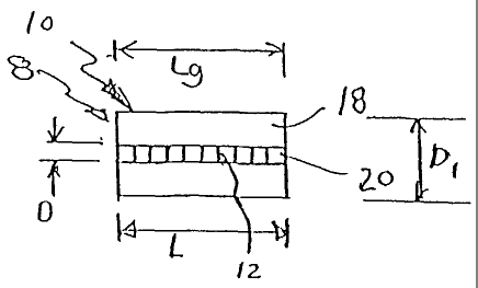
Referring to Fig. l, a diffraction grating-based optical identification
element 8
(or encoded element or coded element) comprises a known optical substrate 10,
S having an optical diffraction grating 12 disposed (or written, impressed,
embedded,
imprinted, etched, grown, deposited or otherwise formed) in the volume of or
on a
surface of a substrate 10. The grating 12 is a periodic or aperiodic variation
in the
effective refractive index and/or effective optical absorption of at least a
portion of the
substrate 10.
The optical identification element described herein is the same as that
described in Copending Patent Application Serial No. (CiDRA Docket No. CC-
0648A), filed contemporaneously herewith, which is incorporated herein by
reference
in its entirety.
In particular, the substrate 10 has an inner region 20 where the grating 12 is
1 S , located. The inner region 20 may be photosensitive to allow the writing
or impressing
of the grating 12. T'he substrate 10 has an outer region 18 which does not
have the
grating 12 therein.
The grating 12 is a combination of one or more individual spatial periodic
sinusoidal variations (or components) in the refractive index that are
collocated at
substantially the same location on the substrate 10 along the length of the
grating
region 20, each having a spatial period (or pitch) A. The resultant
combination of
these individual pitches is the grating 12, comprising spatial periods (Al-An)
each
representing a bit in the code. Thus, the grating 12 represents a unique
optically
readable code, made up of bits, where a bit corresponds to a unique pitch A
within the
2S grating 12. Accordingly, for a digital binary (0-1) code, the code is
determined by
which spatial periods (A1-An) exist (or do not exist) in a given composite
grating 12.
The code or bits may also be determined by additional parameters (or
additional
degrees of multiplexing), and other numerical bases for the code may be used,
as
discussed herein and/or in the aforementioned patent application.
CA 02499037 2005-03-14
WO 2004/025562 PCT/US2003/029164
The grating 12 may also be referred to herein as a composite or collocated
grating. Also, the grating 12 may be referred to as a "hologram", as the
grating 12
transforms, translates, or filters an input optical signal to a predetermined
desired
optical output pattern or signal.
The substrate 10 has an outer diameter D 1 and comprises silica glass (Si02)
having the appropriate chemical composition to allow the grating 12 to be
disposed
therein or thereon. Other materials for the optical substrate 10 may be used
if desired.
For example, the substrate 10 may be made of any glass, e.g., silica,
phosphate glass,
borosilicate glass, or other glasses, or made of glass and plastic, or solely
plastic. For
high temperature or harsh chemical applications, the optical substrate 10 made
of a
glass material is desirable. If a flexible substrate is needed, plastic,
rubber or
polymer-based substrate may be used. The optical substrate 10 may be any
material
capable of having the grating 12 disposed in the grating region 20 and that
allows
light to pass through it to allow the code to be optically read.
1 S The optical substrate 10 with the grating 12 has a length L and an outer
diameter D1, and the inner region 20 diameter D. The length L can range from
very
small "microbeads" (or microelements, micro-particles, or encoded particles),
about
1-1000 microns or smaller, to larger "macroelements" for larger applications
(about
1.0 - 1000 mm or greater). In addition, the outer dimension D1 can range from
small
(less than 1000 microns) to large (1.0 -1000 mm and greater). Other dimensions
and
lengths for the substrate 10 and the grating 12 may be used.
The optical substrate 10 with the grating 12 has a length L and an outer
diameter D1, and the inner region 20 diameter D. The length L can range from
very
small (about 1-1000 microns or smaller) to large (about 1.0 - 1000 mm or
greater). In
addition, the outer dimension D1 can range from small (less than 1000 microns)
to
large (1.0 - 1000 mm and greater). Other dimensions and lengths for the
substrate 10
and the grating 12 may be used. Also, the element may be embedded within or
part of
a larger substrate or object. 'The element may also be in the form of a thread
or fiber to
be weaved into a material.
_g_
CA 02499037 2005-03-14
WO 2004/025562 PCT/US2003/029164
The grating 12 may have a length Lg of about the length L of the substrate 10.
Alternatively, the length Lg of the grating 12 may be shorter than the total
length L of
the substrate 10, as shown in Fig. 11.
The outer region 18 is made of pure silica (Si02) and has a refractive index
n2
of about 1.458 (at a wavelength of about 1553 run), and the inner grating
region 20 of
the substrate 10 has dopants, such as germanium and/or boron, to provide a
refractive
index nl of about 1.453, which is less than that of outer region 18 by about
0.005.
Other indices of refraction nl,n2 for the grating region 20 and the outer
region 18,
respectively, may be used, if desired, provided the grating 12 can be
impressed in the
desired grating region 20. For example, the grating region 20 may have an
index of
refraction that is larger than that of the outer region 18 or grating region
20 may have
the same index of refraction as the outer region 18 if desired.
Refernng to Fig. 2, an incident light 24 of a wavelength ~,, e.g., 532 nm from
a
known frequency doubled Nd:YAG laser or 632nm from a known Helium Neon laser,
is incident on the grating 12 in the substrate 10. Any other input wavelength
~, can be
used if desired provided ~, is within the optical transmission range of the
substrate
(discussed more herein and/or in the aforementioned patent application). A
portion of
the input light 24 passes straight through the grating 12, as indicated by a
line 25. The
remainder of the input light 24 is reflected by the grating 12, as indicated
by a line 27
and provided to a detector 29. The output light 27 may be a plurality of
beams, each
having the same wavelength ~, as the input wavelength ~, and each having a
different
output angle indicative of the pitches (Al-An) existing in the grating 12.
Alternatively, the input light 24 may be a plurality of wavelengths and the
output light
27 may have a plurality of wavelengths indicative of the pitches (A1-An)
existing in
the grating 12. Alternatively, the output light may be a combination of
wavelengths
and output angles. The above techniques are discussed in more detail herein
and/or in
the aforementioned patent application.
The detector 29 has the necessary optics, electronics, software and/or
firmware
to perform the functions described herein. In particular, the detector reads
the optical
-9-
CA 02499037 2005-03-14
WO 2004/025562 PCT/US2003/029164
signal 27 diffracted or reflected from the grating 12 and determines the code
based on
the pitches present or the optical pattern, as discussed more herein or in the
aforementioned patent application. An output signal indicative of the code is
provided
on a line 31.
The encoded element 8 may be used to label any desired item, such as large or
small objects, products, solids, powders, liquids, gases, plants, minerals,
and/or
animals, or any combination of one or more thereof. The label may be used for
many
different purposes, such as for sorting, tracking, identification,
verification,
authentication, anti-theft/anti-counterfeit, security/anti-terrorism, or for
other
purposes. In a manufacturing environment, the elements 8 may be used to track
inventory for production information or sales of goods/products.
For any of the labeled items described herein, the encoded elements 8 may be
tiny discrete microbeads (1 to 1000 microns long) embedded into the surface of
the
item or the encoded element 8 may be a long strand of glass or plastic fiber
that is
woven, inserted, impressed, or injected into the item being labeled.
Alternatively, in
the appropriate cases, the diffraction grating 12 may be written or impressed
directly
into the material, as discussed herein. In any case, the properties of the
encoded
element 8 do not change. For labeled items that are pliable, bendable, or
flexible, the
element 8 may be made of a bendable material, such as a polymer or plastic.
Also, if
the item material is soft or compliant the beads may be pressed, pushed,
hammered or
shot into the material, either for side reading or end reading, depending on
the
application.
For any of the embodiments herein, the label on the item can be detected by
scanning the item with incident light and detecting the reflected light as
discussed
herein and/or in the aforementioned patent application. When an element 8 is
embedded or attached to an item that is not reflective or transparent to the
incident
light 24 and reflected light 27, and if the element 8 is not reflective, it
may be
desirable to illuminate the element from an axial end 8 to achieve best
results for code
reading.
-10-
CA 02499037 2005-03-14
WO 2004/025562 PCT/US2003/029164
In general, the encoded elements 8 may be used to label any products or
components within a product and may be used for product manufacturing/
production
identification.
Refernng to Fig. 3, illustrations (a)-(d), encoded elements 8 may be used to
label glass or plastic items, such as microscope slides 811, test tubes 813,
beakers
815, cookware 817, 'storage containers andlor covers, mufti-well plates, micro-
well
plates, plastic bags, windshields, windows, glasses, contact lenses, other
lenses,
optical components, tape, bottles, displays, display cases, watch faces,
mirrors,
sample or pietri dishes, or any other item made of a material that is
transparent or
substantially transparent to the incident light 24 and reflected light 27 used
for read
the code in the encoded elements 8. The invention may be used to identify such
glass
or plastic items by writing the diffraction grating 12 directly into the
material or by
embedding into or otherwise attaching the encoded elements 8 to the item. In
the case
where the code is written directly into the material, the material must have
sufficient
photosensitivity to allow the diffraction grating 12 to be written into the
material with
sufficient strength so the code can be optically read. We have found that
borosilicate
glass has sufficient photosensitivity to support the creation of a diffraction
grating 12
therein. Other glasses may be used.
Referring to Fig. 4, illustrations (a) and (b), the encoded elements 8 may be
used to label micron size products, such as, microcircuits computer chips,
integrated
circuits (IC's), or other small products or portions thereof. Referring to
Fig. 4,
illustration (c), the elements 8 may also be used to label silicon wafers 59
or small
portions or regions 57 thereof before being cut into small devices or
microcircuits.
Referring to Fig. 5, the elements 8 may be used to label any single or
multiple
cells 101 that are attached to or otherwise disposed on the element 8. The
cells 101
may include: molecules, particles, elements, compounds, organisms, atoms,
chemicals, acids, bases, nucleic acids, chemical libraries, DNA,
polynucleotides,
oligorners, RNA, proteins, peptides, polymers, hydrocarbons, or other cells.
The cells
11-
CA 02499037 2005-03-14
WO 2004/025562 PCT/US2003/029164
101 may be alive or dead, organic or inorganic, and may be individual or
groups or
chains of cells and may change or mutate over time.
Refernng to Fig. 6, illustrations, (a)-(d), the encoded elements 8 may be used
to label a liquid or liquid products located in a container 801 or in an open
or closed
flowing pipe or conduit 803, 805 respectively. In that case, the elements 8
are mixed
with the liquid. In addition, the elements 8 may also be used to label
powders, such as
powdered detergent, dirt, pulverized coal, gunpowder, anthrax, or any other
powders
located in a container 807, or in an open or closed flowing pipe or conduit
803,805,
respectively. Also, the elements 8 may be used to label or identify any
combination of
fluids (liquids and/or gases) and/or powders. Also, the elements 8 may be used
to
label gases, such as gases in containers or gases flowing in a pipe or
conduit, or
gaseous by-products of reactions, such as combustion exhaust or other exhaust.
Also,
the elements 8 may be used to label liquid particles or droplets in gas, such
as steam.
The elements 8 may be used to track the flow of a liquid, powder, gas, etc. in
an
industrial plant to determine where the liquid is flowing or has flown.
The elements 8 may be removed from a fluid, powder and/or gas solution or
mixture other material by electro-magnetic attraction (if the elements are
electro-
magnetic), skimmed off the surface (if the elements 8 are less dense than the
solution,
i.e., buoyant or semi-buoyant), or from settling to the bottom of a container
(if the
elements 8 are more dense than the solution), or by filtering the solution
with a
strainer or filter.
The elements 8 can placed in a fluid or powder and the fluid or powder is used
for labeling an item. For example, the elements 8 may be mixed with paint (or
other
adhesive fluid) and sprayed on an item, such as a car or boat (see Fig. 7,
illustrations
(b) and (c)) or any other item that can be sprayed or painted. The same may be
done
with a dry powder that is sprayed on a newly painted or otherwise adhesive
surface, or
with an adhesive powder that is sprayed on a dry, or painted or adhesive
surface.
Refernng to Fig. 7, illustrations (a), (b), (c), (f), (g), and (h), in
particular, the
encoded elements 8 may be used to label large and/or valuable items such as
cases
-12-
CA 02499037 2005-03-14
WO 2004/025562 PCT/US2003/029164
841 (e.g., suitcases, briefcases, garment bags, and the like), cars 831, boats
833,
paintings 835, china 837, jewelry 839, and the like. Also, the elements 8 may
be used
as a way of putting the vehicle identification number (VIN) or other similar
identification information in a hidden location and/or in many locations on an
item
that can only be read by the proper equipment.
Referring to Fig. 7, illustrations (d), (e), and (r), the encoded elements 8
may
also be used to label currency 829, coins, bills, or credit cards. Also, the
elements 8
may be used an alternative or addition to magnetic strips currently used on
many
types of cards 825, e.g., access cards, key cards, ID cards, debit cards,
credit cards,
and the like. In addition, the elements 8 may be used as part of a key 827.
Referring to Fig. 7, illustration (i), the elements 8 may be used to label
food
containers 847 and the like.
Refernng to Fig. 7, illustrations (j) and (1), the elements 8 may be used to
label
building materials 843, e.g., wood, pressboard, composite boards (e.g., made
of wood,
plastic, and/or metal particles), sheetrock, wallboard, wallpaper, molding,
tiles and the
like or other building materials. Similarly, the elements 8 may be used to
label
furniture or other home or office furnishings 845.
Refernng to Fig. 7, illustrations (m), (o), arid (p), the encoded elements 8
may
be used to label any animals 649, creatures, people/humans 855, andlor plants,
or
parts thereof 853. Such a label could be used in addition to or instead of
fingerprints,
retina scans, DNA or other identification techniques or labels.
Refernng to Fig. 7, illustrations (n) and (q), the encoded elements 8 may be
used to label documents 857, books 851, and/or packages.
Referring to Fig. 7, illustrations (s) and (t), the encoded elements 8 may be
used to label weapons, ammunition, explosive devices, guns 819, artillery,
bullets
821, mortar, grenades, missiles, torpedoes, projectiles, fireworks, bombs,
spacecraft,
aircraft, satellites, jet engines, submarines and tanks.
Referring to Fig. 7, illustration (u), the encoded elements 8 may be used to
label clothing 823, garments, uniforms, linens, leather, footware, headgear,
or textiles.
-13-
CA 02499037 2005-03-14
WO 2004/025562 PCT/US2003/029164
Referring to Fig. 7, illustration (v), the encoded elements 8 may be used to
label storage media, such as compact discs and digital video discs (DVD's), or
any
other devices that uses light to read information, video or audio tapes tapes,
disc
drives, and the like.
Referring to Fig. 8, the code may be a simple code or may be a more complex
code having many pieces of information located in the code. In addition, the
code may
have checks within the code to ensure the code is read correctly. It can be
viewed as a
serial digital message, word, or frame consisting of N bits.
In particular, there may be start and stop bits 869, 871, respectively. The
start
and stop bits may each take up more than one bit location if desired. In
addition there
may be an error check portion of the message, such as a check sum or CRC
(cyclic
redundancy check) having a predetermined number of bits, and a code section
873
having a predetermined number of bits. The error check portion ensures that
the code
which is obtained from the bead is accurate. Accordingly, having a large
number of
1 S bits in the element 8 allows for greater statistical accuracy in the code
readout and
decreases the likelihood of providing an erroneous code. Accordingly, if a
code
cannot be read without an error, no code will be provided, avoiding an
erroneous
result. Any known techniques for digital error checking for single or rnulti-
bit errors
may be used.
The code section 873 may be broken up into one or more groups of bits, for
example, three bit groups 863,865,867, each bit group containing information
about
the bead itself or the item attached to the bead or how the bead is to be
used, or other
information. For example, the first bit group 863 may contain information
regarding
"identifying numbers", such as: lot number, quality control number, model
number,
serial number, inventory control number; the second bit group 865 may contain
"type" information, such as: chemical or cell type, experiment type, item
type, animal
type; and the third bit group 867 may contain "date" information, such as:
manufactured date, experiment date, creation date, initial tracking date. Any
other bit
-14-
CA 02499037 2005-03-14
WO 2004/025562 PCT/US2003/029164
groups, number of bit groups, or size of bit groups may be used if desired.
Also,
additional error or fault checking can be used if desired.
In particular, for a product manufacturing application, the code may have the
serial number, the lot number, date of manufacture, etc. or have other
information that
identifies the item and/or information about the item. For a chemical or assay
application, the code may have information about the chemical attached to the
bead, ,
the date and/or time of creation of the chemical or experiment, or other
information of
interest.
ulmulinirllrulilmulmrmm
Referring to Fig. 9, The reflected light 27, comprises a plurality of beams 26-
36 that pass through a lens 37, which provides focused light beams 46-56,
respectively, which are imaged onto a CCD camera 60. The lens 37 and the
camera
60, and any other necessary electronics or optics for performing the functions
described herein, make up the reader 29. Instead of or in addition to the lens
37, other
1 S imaging optics may be used to provide the desired characteristics of the
optical
image/signal onto the camera 60 (e.g., spots, lines, circles, ovals, etc.),
depending on
the shape of the substrate 10 and input optical signals. Also, instead of a
CCD camera
other devices may be used to read/capture the output light.
Refernng to Fig. 10, the image on the CCD camera 60 is a series of
illuminated stripes indicating ones and zeros of a digital pattern or code of
the grating
12 in the element 8. Refernng to Fig. 1 l, lines 68 on a graph 70 are
indicative of a
digitized version of the image of Fig. 10 as indicated in spatial periods (A1-
An).
Each of the individual spatial periods (A1-An) in the grating 12 is slightly
different, thus producing an array of N unique diffraction conditions (or
diffraction
angles) discussed more hereinafter. When the element 8 is illuminated from the
side,
in the region of the grating 12, at an appropriate input angle, e.g., about 30
degrees,
with a single input wavelength ~, (monochromatic) source, the diffracted (or
reflected)
beams 26-36 are generated. Other input angles Ai may be used if desired,
depending
-15-
CA 02499037 2005-03-14
WO 2004/025562 PCT/US2003/029164
on various design parameters as discussed herein and/or in the aforementioned
patent
application, and provided that a known diffraction equation (Eq. 1 below) is
satisfied:
sin(6; ) + sin(Bo ) = m~. / nA Eq. 1
where Eq. 1 is diffraction (or reflection or scatter) relationship between
input
wavelength ~,, input incident angle 0i, output incident angle 00, and the
spatial period
A of the grating 12. Further, m is the "order" of the reflection being
observed, and n is
the refractive index of the substrate 10. The value of m=1 or first order
reflection is
acceptable for illustrative purposes. Eq. 1 applies to light incident on outer
surfaces of
the substrate 10 which are parallel to the longitudinal axis of the grating
(or the kB
vector). Because the angles 0i,0o are defined outside the substrate 10 and
because the
effective refractive index of the substrate 10 is substantially a common
value, the
value of n in Eq. 1 cancels out of this equation.
Thus, for a given input wavelength ~,, grating spacing A, and incident angle
of
the input light 0i, the angle Oo of the reflected output light may be
determined.
Solving Eq. 1 for 0o and plugging in m=l, gives:
Bo =sin ~(.1/~l-sin(~i)) Eq. 2
For example, for an input wavelength ~. = 532 nm, a grating spacing A= 0.532
microns (or 532 nm), and an input angle of incidence 8i =30 degrees, the
output angle
of reflection will be 80 = 30 degrees. Alternatively, for an input wavelength
~, = 632
nm, a grating spacing A = 0.532 microns (or 532 nm), and an input angle 0i of
30
degrees, the output angle of reflection 0o will be at 43.47 degrees, or for an
input
angle 0i = 37 degrees, the output angle of reflection will be 00 = 37 degrees.
Any
input angle that satisfies the design requirements discussed herein and/or in
the
aforementioned patent application may be used.
In addition, to have sufficient optical output power and signal to noise
ratio,
the output light 27 should fall within an acceptable portion of the Bragg
envelope (or
normalized reflection efficiency envelope) curve 200, as indicated by points
204,206,
-16-
CA 02499037 2005-03-14
WO 2004/025562 PCT/US2003/029164
also defined as a Bragg envelope angle 8B, as also discussed herein and/or in
the
aforementioned patent application. The curve 200 may be defined as:
I (ki, ko) ~ ~KD~Z sin cz (ki -~ o)D Eq. 3
where K = 2~8n/~,, where, 8n is the local refractive index modulation
amplitude of the
grating and ~, is the input wavelength, sinc(x) = sin(x)/x, and the vectors k;
_
2~cos(0;)/~, and ko= 2~cos (00)/x, are the projections of the incident light
and the
output (or reflected) light, respectively, onto the line 203 normal to the
axial direction
of the grating 12 (or the grating vector ks), D is the thickness or depth of
the grating
12 as measured along the line 203 (normal to the axial direction of the
grating 12).
Other substrate shapes than a cylinder may be used and will exhibit a similar
peaked
characteristic of the Bragg envelope. We have found that a value for Sn of
about 10~
in the grating region of the substrate is acceptable; however, other values
may be used
if desired.
Rewriting Eq. 3 gives the reflection efficiency profile of the Bragg envelope
as:
I(ki ko)~~2~~SjmD~2~Sin(x)~Z Eq.4
' ~, ~j -~Ix
where: x =(ki-ko)Dl2 = (~tDl~,) *(cos ~ i - cos B o)
Thus, when the input angle 8i is equal to the output (or reflected) angle 80
(i.e., 8i = 8a), the reflection efficiency I (Eqs. 3 & 4) is maximized, which
is at the
center or peak of the Bragg envelope. When 8i = 80, the input light angle is
referred
to as the Bragg angle as is known. 'The efficiency decreases for other input
and output
angles (i.e., 8i ~ 8~), as defined by Eqs. 3 & 4. Thus, for maximum reflection
efficiency and thus output light power, for a given grating pitch A and input
wavelength, the angle 8i of the input light 24 should be set so that the angle
80 of the
reflected output light equals the input angle 0i.
-17-
CA 02499037 2005-03-14
WO 2004/025562 PCT/US2003/029164
Also, as the thickness or diameter D of the grating decreases, the width of
the
sin(x)/x function (and thus the width of the Bragg envelope) increases and,
the
coefficient to or amplitude of the since (or (sin(x)/x) 2 function (and thus
the efficiency
level across the Bragg envelope) also increases, and vice versa. Further, as
the
wavelength ~, increases, the half width of the Bragg envelope as well as the
efficiency
level across the Bragg envelope both decrease. Thus, there is a trade-off
between the
brightness of an individual bit and the number of bits available under the
Bragg
envelope. Ideally, 8n should be made as large as possible to maximize the
brightness,
which allows D to be made smaller.
From Eq. 3 and 4, the half angle of the Bragg envelope 8B is defined as:
__
B ~D sin(9i ) Eq. S
where r~ is a reflection efficiency factor which is the value for x in the
sinc2(x)
function where the value of sinc2(x) has decreased to a predetermined value
from the
maximum amplitude as indicated by points 204,206 on the curve 200.
We have found that the reflection efficiency is acceptable when r~ <_ 1.39.
This
value for ri corresponds to when the amplitude of the reflected beam (i.e.,
from the
sinc2(x) function of Eqs. 3 & 4) has decayed to about 50% of its peak value.
In
particular, when x = 1.39 = rl, sinca(x) = 0.5. However, other values for
efficiency
thresholds or factor in the Bragg envelope may be used if desired.
The beams 26-36 are imaged onto the CCD camera 60 to produce the pattern
of light and dark regions 120-132 representing a digital (or binary) code,
where light
= 1 and dark = 0 (or vice versa). The digital code may be generated by
selectively
creating individual index variations (or individual gratings) with the desired
spatial
periods Al-An. Other illumination, readout techniques, types of gratings,
geometries,
materials, etc. may be used as discussed in the aforementioned patent
application.
Refernng to Fig.l2, illustrations (a)-(c), for the grating 12 in a cylindrical
substrate 10 having a sample spectral 17 bit code (i.e., 17 different pitches
A1-A17),
-lg-
CA 02499037 2005-03-14
WO 2004/025562 PCT/US2003/029164
the corresponding image on the CCD (Charge Coupled Device) camera 60 is shown
for a digital pattern of 7 bits turned on (10110010001001001); 9 bits turned
on of
(11000101010100111); all 17 bits turned on of (11111111111111111).
For the images in Fig. 12, the length of the substrate 10 was 450 microns, the
S outer diameter D1 was 65 microns, the inner diameter D was 14 microns, 8n
for the
grating 12 was about 10~, n1 in portion 20 was about 1.458 (at a wavelength of
about
1550 nm), n2 in portion 18 was about 1.453, the average pitch spacing A for
the
grating 12 was about 0.542 microns, and the spacing between pitches dA was
about
0.36 % of the adjacent pitches A. _
Referring to Fig. 13, illustration (a), the pitch A of an individual grating
is the
axial spatial period of the sinusoidal variation in the refractive index nl in
the region
of the substrate 10 along the axial length of the grating 12 as indicated by a
curve
90 on a graph 91. Refernng to Fig. 13, illustration (b), a sample composite
grating 12
comprises three individual gratings that are co-located on the substrate 10,
each
15 individual grating having slightly different pitches, Al, A2, A3,
respectively, and the
difference (or spacing) DA between each pitch A being about 3.0 % of the
period of
an adjacent pitch A as indicated by a series of curves 92 on a graph 94.
Referring to
Fig. 13, illustration (c), three individual gratings, each having slightly
different
pitches, Al, A2, A3, respectively, are shown, the difference M between each
pitch A
20 being about 0.3% of the pitch A of the adjacent pitch as shown by a series
of curves
95 on a graph 97. The individual gratings in Fig. 13, illustrations (b) and
(c) are
shown to all start at 0 for illustration purposes; however, it should be
understood that,
the separate gratings need not all start in phase with each other. Referring
to Fig. 13,
illustration (d), the overlapping of the individual sinusoidal refractive
index variation
pitches Al-An in the grating region 20 of the substrate 10, produces a
combined
resultant refractive index variation in the composite grating 12 shown as a
curve 96 on
a graph 98 representing the combination of the three pitches shown in Fig. 13,
illustration (b). Accordingly, the resultant refractive index variation in the
grating
-19-
CA 02499037 2005-03-14
WO 2004/025562 PCT/US2003/029164
region 20 of the substrate 10 may not be sinusoidal and is a combination of
the
individual pitches A (or index variation).
The maximum number of resolvable bits N, which is equal to the number of
different grating pitches A (and hence the number of codes), that can be
accurately
read (or resolved) using side-illumination and side-reading of the grating 12
in the
substrate 10, is determined by numerous factors, including: the beam width w
incident
on the substrate (and the corresponding substrate length L and grating length
Lg), the
thickness or diameter D of the grating 12, the wavelength ~, of incident
light, the beam
divergence angle 0R, and the width of the Bragg envelope OB (discussed more in
the
aforementioned patent application), and may be determined by the equation:
_ r~~3L q
2 D sin( B; ) E . 6
Refernng to Fig. 14, instead of having the input light 24 at a single
wavelength
~, (monochromatic) and reading the bits by the angle Ao of the output light,
the bits (or
grating pitches A) may be read/detected by providing a plurality of
wavelengths and
1 S reading the wavelength spectrum of the reflected output light signal. In
this case, there
would be one bit per wavelength, and thus, the code is contained in the
wavelength
information of the reflected output signal.
In this case, each bit (or A) is defined by whether its corresponding
wavelength falls within the Bragg envelope, not by its angular position within
the
Bragg envelope 200. As a result, it is not limited by the number of angles.
that can fit
in the Bragg envelope 200 for a given composite grating 12, as in the
embodiment
discussed hereinbefore. Thus, using multiple wavelengths, the only limitation
in the
number of bits N is the maximum number of grating pitches A that can be
superimposed and optically distinguished in wavelength space for the output
beam.
Referring to Figs. 14 and 15, illustration (a), the reflection wavelength
spectrum (~,1-~.n) of the reflected output beam 310 will exhibit a series of
reflection
peaks 695, each appearing at the same output Bragg angle 80. Each wavelength
peak
-20-
CA 02499037 2005-03-14
WO 2004/025562 PCT/US2003/029164
695 (~,1-~,n) corresponds to an associated spatial period (A1-An), which make
up the
grating 12.
One way to measure the bits in wavelength space is to have the input light
angle 0i equal to the output light angle 00, which is kept at a constant
value, and to
provide an input wavelength ~, than satisfies the diffraction condition (Eq.
1) for each
grating pitch A. This will maximize the optical power of the output signal for
each
pitch A detected in the grating 12.
Refernng to 15, illustration (b), the transmission wavelength spectrum of the
transmitted output beam 330 (which is transmitted straight through the grating
12)
will exhibit a series of notches (or dark spots) 696. Alternatively, instead
of detecting
the reflected output light 310, the transmitted light 330 may be detected at
the
detector/reader 308. It should be understood that the optical signal levels
for the
reflection peaks 695 and transmission notches 696 will depend on the
"strength" of
the grating 12, i.e., the magnitude of the index variation n in the grating
12.
In Fig. 14, the bits may be detected by continuously scanning the input
wavelength. A known optical source 300 provides the input light signal 24 of a
coherent scanned wavelength input light shown as a graph 304. The source 300
provides a sync signal on a line 306 to a known reader 308. The sync signal
may be a
timed pulse or a voltage ramped signal, which is indicative of the wavelength
being
provided as the input light 24 to the substrate 10 at any given time. The
reader 308
may be a photodiode, CCD camera, or other optical detection device that
detects
when an optical signal is present and provides an output signal on a line 309
indicative of the code in the substrate 10 or of the wavelengths present in
the output
light, which is directly related to the code, as discussed herein. The grating
12 reflects
the input light 24 and provides an output light signal 310 to the reader 308.
The
wavelength of the input signal is set such that the reflected output light 310
will be
substantially in the center 314 of the Bragg envelope 200 for the individual
grating
pitch (or bit) being read.
-21 -
CA 02499037 2005-03-14
WO 2004/025562 PCT/US2003/029164
Alternatively, the source 300 may provide a continuous broadband wavelength
input signal such as that shown as a graph 316. In that case, the reflected
output beam
310 signal is provided to a narrow band scanning filter 318 which scans across
the
desired range of wavelengths and provides a filtered output optical signal 320
to the
reader 308. The filter 318 provides a sync signal on a line 322 to the reader,
which is
indicative of which wavelengths are being provided on the output signal 320 to
the
reader and may be similar to the sync signal discussed hereinbefore on the
line 306
from the source 300. In this case, the source 300 does not need to provide a
sync
signal because the input optical signal 24 is continuous. Alternatively,
instead of
having the scanning filter being located in the path of the output beam 310,
the
scanning filter may be located in the path of the input beam 24 as indicated
by the
dashed box 324, which provides the sync signal on a line 323.
Alternatively, instead of the scanning filters 318,324, the reader 308 may be
a
known optical spectrometer (such as a known spectrum analyzer), capable of
measuring the wavelength of the output light.
The desired values for the input wavelengths ~, (or wavelength range) for the
input signal 24 from the source 300 may be determined from the Bragg condition
of
Eq. 1, for a given grating spacing A and equal angles for the input light Oi
and the
angle light 80. Solving Eq. 1 for ~, and plugging in rn=1, gives:
a, =A ~sin(6 0)+ sin(B i)J Eq. 7
It is also possible to combine the angular-based code detection with the
wavelength-based code detection, both discussed hereinbefore. In this case,
each
readout wavelength is associated with a predetermined number of bits within
the
Bragg envelope. Bits (or grating pitches A) written for different wavelengths
do not
show up unless the correct wavelength is used.
Accordingly, the bits (or grating pitches A) can be read using one wavelength
and many angles, many wavelengths and one angle, or many wavelengths and many
angles.
-22-
CA 02499037 2005-03-14
WO 2004/025562 PCT/US2003/029164
Referring to Fig. 16, the grating 12 may have a thickness or depth D which is
comparable or smaller than the incident beam wavelength ~,. This is known as a
"thin"
diffraction grating (or the full angle Bragg envelope is 180 degrees). In that
case, the
half angle Bragg envelope 8B is substantially 90 degrees; however, 8n must be
made
large enough to provide sufficient reflection efficiency, per Eqs. 3 and 4. In
particular,
for a "thin" grating, D*8n ~ 7J2, which corresponds to a ~ phase shift between
adjacent minimum and maximum refractive index values of the grating 12.
It should be understood that there is still a trade-off discussed hereinbefore
with beam divergence angle 6R and the incident beam width (or length L of the
substrate), but the accessible angular space is theoretically now 90 degrees.
Also, for
maximum efficiency, the phase shift between adjacent minimum and maximum
refractive index values of the grating 12 should approach a ~ phase shift;
however,
other phase shifts may be used.
In this case, rather than having the input light 24 coming in at the
conventional
Bragg input angle Oi, as discussed hereinbefore and indicated by a dashed line
701,
the grating 12 is illuminated with the input light 24 oriented on a line 705
orthogonal
to the longitudinal grating vector 705. The input beam 24 will split into two
(or more)
beams of equal amplitude, where the exit angle 6o can be determined from Eq. 1
with
the input angle 0; 0 (normal to the longitudinal axis of the grating 12).
In particular, from Eq. l, for a given grating pitch Al, the +/-1St order
beams
(m=+1 and m=-1), corresponds to output beams 700,702, respectively. For the +/-
2°d
order beams (m=+2 and m=-2), corresponds to output beams 704,706,
respectively.
'The Ot" order (undefracted) beam (m=0), corresponds to beam 708 and passes
straight
through the substrate. The output beams 700-708 project spectral spots or
peaks 710-
718, respectively, along a common plane, shown from the side by a line 709,
which is
parallel to the upper surface of the substrate 10.
For example, for a grating pitch A = 1.0 um, and an input wavelength ~, = 400
nrn, the exit angles 9o are ~ +/- 23.6 degrees (for m = +/-1 ), and +/- 53.1
degrees
- 23 -
CA 02499037 2005-03-14
WO 2004/025562 PCT/US2003/029164
(from m = +/-2), from Eq. 1. It should be understood that for certain
wavelengths,
certain orders (e.g., m = +/- 2) may be reflected back toward the input side
or
otherwise not detectable at the output side of the grating 12.
Alternatively, one can use only the +/-ls' order (m = +/-1) output beams for
the
code, in which case there would be only 2 peaks to detect, 712, 714.
Alternatively,
one can also use any one or more pairs from any order output beam that is
capable of
being detected. Alternatively, instead of using a pair of output peaks for a
given order,
an individual peak may be used.
Referring to Fig. 17, if two pitches A1,A2 exist in the grating 12, two sets
of
peaks will exist. In particular, for a second grating pitch A2, the +/-ls'
order beams
(m=+1 and m=-1), corresponds to output beams 720,722, respectively. For the +/-
2°a
order beams (m=+2 and m=-2), corresponds to output beams 724,726,
respectively.
The 0'" order (un-defracted) beam (rn=0), corresponds to beam 718 and passes
straight
through the substrate. The output beams 720-726 corresponding to the second
pitch
1 S A2 project spectral spots or peaks 730-736, respectively, which are at a
different
location than the point 710-716, but along the same common plane, shown from
the
side by the line 709.
Thus, for a given pitch A (or bit) in a grating, a set of spectral peaks will
appear at a specific location in space. Thus, each different pitch corresponds
to a
different elevation or output angle which corresponds to a predetermined set
of
spectral peaks. Accordingly, the presence or absence of a particular peak or
set of
spectral peaks defines the code.
In general, if the angle of the grating 12 is not properly aligned with
respect to
the mechanical longitudinal axis of the substrate 10, the readout angles may
no longer
be symmetric, leading to possible difficulties in readout. With a thin
grating, the
angular sensitivity to the alignment of the longitudinal axis of the substrate
10 to the
input angle ~i of incident radiation is reduced or eliminated. In particular,
the input
light can be oriented along substantially any angle Oi with respect to the
grating 12
without causing output signal degradation, due the large Bragg angle envelope.
Also,
-24-
CA 02499037 2005-03-14
WO 2004/025562 PCT/US2003/029164
if the incident beam 24 is normal to the substrate 10, the grating 12 can be
oriented at
any rotational (or azimuthal) angle without causing output signal degradation.
However, in each of these cases, changing the incident angle 0i will affect
the output
angle 00 of the reflected light in a predetermined predictable way, thereby
allowing
for accurate output code signal detection or compensation.
Referring to Fig. 18, for a thin grating, in addition to multiplexing in the
elevation or output angle based on grating pitch A, the bits can also be
multiplexed in
an azimuthal (or rotational) angle 0a of the substrate. In particular, a
plurality of
gratings 750,752,754,756 each having the same pitch A are disposed in a
surface 701
of the substrate 10 and located in the plane of the substrate surface 701. The
input
light 24 is incident on all the gratings 750,752,754,756 simultaneously. Each
of the
gratings provides output beams oriented based on the grating orientation. For
example, the grating 750 provides the output beams 764,762, the grating 752
provides
the output beams 766,768, the grating 754 provides the output beams 770,772,
and the
grating 756 provides the output beams 774,776. Each of the output beams
provides
spectral peaks or spots (similar to that discussed hereinbefore), which are
located in a
plane 760 that is parallel to the substrate surface plane 701. In this case, a
single
grating pitch A can produce many bits depending on the number of gratings that
can
be placed at different azimuthal (rotational) angles on the surface of the
substrate 10
and the number of output beam spectral peaks that can be spatially and
optically
resolved/detected. Each bit may be viewed as the presence or absence of a pair
of
peaks located at a predetermined location in space in the plane 760. Note that
this
example uses only the m = +/-1 S' order for each reflected output beam.
Alternatively,
the detection may also use the m = +/-2"d order. In that case, there would be
two
additional output beams and peaks (not shown) for each grating (as discussed
hereinbefore) that rnay lie in the same plane as the plane 760 and may be on a
concentric circle outside the circle 760.
In addition, the azimuthal multiplexing can be combined with the elevation or
output angle multiplexing discussed hereinbefore to provide two levels of
- 25 -
CA 02499037 2005-03-14
WO 2004/025562 PCT/US2003/029164
multiplexing. Accordingly, for a thin grating, the number of bits can be
multiplexed
based on the number of grating pitches A and/or geometrically by the
orientation of
the grating pitches.
Furthermore, if the input light angle 0i is normal to the substrate 10, the
edges
of the substrate 10 no longer scatter light from the incident angle into the
"code
angular space", as discussed herein and/or in the aforementioned patent
application.
Also, in the thin grating geomehy, a continuous broadband wavelength source
may be used as the optical source if desired.
Referring to Fig. 19, instead of or in addition to the pitches A in the
grating 12
being oriented normal to the longitudinal axis, the pitches rnay be created at
a angle
Og. In that case, when the input light 24 is incident normal to the surface
792, will
produce a reflected output beam 790 having an angle 0o determined by Eq. 1 as
adjusted for the blaze angle 8g. This can provide another level of
multiplexing bits in
the code.
Referring to Fig. 20, instead of using an optical binary (0-1) code, an
additional level of multiplexing may be provided by having the optical code
use other
numerical bases, if intensity levels of each bit are used to indicate code
information.
This could be achieved by having a corresponding magnitude (or strength) of
the
refractive index change (8n) for each grating pitch A. Four intensity ranges
are shown
for each bit number or pitch A, providing for a Base-4 code (where each bit
corresponds to 0,1,2, or 3). The lowest intensity level, corresponding to a 0,
would
exist when this pitch A is not present in the grating 12. The next intensity
level 450
would occur when a first low level 8n1 exists in the grating that provides an
output
signal within the intensity range corresponding to a 1. The next intensity
level 452
would occur when a second higher level 8n2 exists in the grating 12 that
provides an
output signal within the intensity range corresponding to a 2. The next
intensity level
452, would occur when a third higher level 8n3 exists in the grating 12 that
provides
an output signal within the intensity range corresponding to a 3.
-26-
CA 02499037 2005-03-14
WO 2004/025562 PCT/US2003/029164
Refernng to Fig. 21, the input light 24 may be incident on the substrate 10 on
an end face 600 of the substrate 10. In that case, the input light 24 will be
incident on
the grating 12 having a more significant component of the light (as compared
to side
illumination discussed hereinbefore) along the longitudinal grating axis 207
of the
grating (along the grating vector kB), as shown by a line 602. The light 602
reflects
off the grating 12 as indicated by a line 604 and exits the substrate as
output light 608.
Accordingly, it should be understood by one skilled in the art that the
diffraction
equations discussed hereinbefore regarding output diffraction angle 8o also
apply in
this case except that the reference axis would now be the grating axis 207.
Thus, in
this case, the input and output light angles Oi,Oo, would be measured from the
grating
axis 207 and length Lg of the grating 12 would become the thickness or depth D
of
the grating 12. As a result, a grating 12 that is 400 microns long, would
result in the
Bragg envelope 200 being narrow. It should be understood that because the
values of
nl and n2 are close to the same value, the slight angle changes of the light
between
the regions 18,20 are not shown herein.
In the case where incident light 610 is incident along the same direction as
the
grating vector (Kb) 207, i.e., 0i=0 degrees, the incident light sees the whole
length Lg
of the grating 12 and the grating provides a reflected output light angle 80 =
0
degrees, and the Bragg envelope 612 becomes extremely narrow, as the narrowing
effect discussed above reaches a limit. In that case, the relationship between
a given
pitch A in the grating 12 and the wavelength of reflection ~, is governed by a
known
"Bragg grating" relation:
~ = 2 ~,ll-A Eq. 8
where ne~is the effective index of refraction of the substrate, ~, is the
input (and
output wavelength) and A is the pitch. This relation, as is known, may be
derived
from Eq. 1 where 8i = 80 = 90 degrees.
In that case, the code information is readable only in the spectral wavelength
of the reflected beam, similar to that discussed hereinbefore for wavelength
based
code reading. Accordingly, the input signal in this case may be a scanned
wavelength
-27-
CA 02499037 2005-03-14
WO 2004/025562 PCT/US2003/029164
source or a broadband wavelength source. In addition, as discussed
hereinbefore for
wavelength based code reading, the code information may be obtained in
reflection
from the reflected beam 614 or in transmission by the transmitted beam 616
that
passes through the grating 12.
It should be understood that for shapes of the substrate 10 or element 8 other
than a cylinder, the effect of various different shapes on the propagation of
input light
through the element 8, substrate 10, andlor grating 12, and the associated
reflection
angles, can be determined using known optical physics including Snell's Law,
shown
below:
n;~ sin Oin = no"~ sin Oout Eq. 9
where n;" is the refractive index of the first (input) medium, and no"t is the
refractive index of the second (output) medium, and Gin and Gout are measured
from a
line 620 normal to an incident surface 622.
Referring to Fig. 22, if the value of nl in the grating region 20 is greater
than
the value of n2 in the non-grating region 18, the grating region 20 of the
substrate 10
will act as a known optical waveguide for certain wavelengths. In that case,
the
grating region 20 acts as a "core" along which light is guided and the outer
region 18
acts as a "cladding" which helps confine or guide the light. Also, such a
waveguide
will have a known "numerical aperture" (Ona) that will allow light that is
within the
aperture Ona to be directed or guided along the grating axis 207 and reflected
axially
off the grating 12 and returned and guided along the waveguide. In that case,
the
grating 12 will reflect light having the appropriate wavelengths equal to the
pitches A
present in the grating 12 back along the region 20 (or core) of the waveguide,
and
pass the remaining wavelengths of light as the light 632. Thus, having the
grating
region 20 act as an optical waveguide for wavelengths reflected by the grating
12
allows incident light that is not aligned exactly with the grating axis 207 to
be guided
along and aligned with the grating 12 axis 207 for optimal grating reflection.
If an optical waveguide is used any standard waveguide may be used, e.g., a
standard telecommunication single mode optical fiber (125 micron diameter or
80
_2g_
CA 02499037 2005-03-14
WO 2004/025562 PCT/US2003/029164
micron diameter fiber with about a 8-10 micron diameter), or a larger diameter
waveguide (greater than 0.5 mm diameter), such as is describe in U.S. Patent
Application, Serial No. 09/455,868, filed December 6, 1999, entitled "Large
Diameter
Waveguide, Grating". Further, any type of optical waveguide may be used for
the
S optical substrate 10, such as, a mufti-mode, birefringent, polarization
maintaining,
polarizing, mufti-core, mufti-cladding, or microsturctured optical waveguide,
or a flat
or planar waveguide (where the waveguide is rectangular shaped), or other
waveguides.
Refernng to Fig. 23, if the grating 12 extends across the entire dimension D
of
the substrate, the substrate 10 does not behave as a waveguide for the
incident or
reflected light and the incident light 24 will be diffracted (or reflected) as
indicated by
lines 642, and the codes detected as discussed hereinbefore for the end-
incidence
condition discussed hereinbefore with Fig. 45, and the remaining light 640
passes
straight through.
Refernng to Fig. 24, illustrations (a)-(c), in illustration (a), for the end
illumination condition, if a blazed or angled grating is used, as discussed
hereinbefore, the input light 24 is coupled out of the substrate 10 at a known
angle as
shown by a line 650. Refernng to Fig. 24, illustration (b), alternatively, the
input light
24 may be incident from the side and, if the grating 12 has the appropriate
blaze
angle, the reflected light will exit from the end face 652 as indicated by a
line 654.
Refernng to Fig. 24, illustration (c), the grating 12 may have a plurality of
different
pitch angles 660,662, which reflect the input light 24 to different output
angles as
indicated by lines 664, 666. This provides another level of multiplexing
(spatially)
additional codes, if desired.
The grating 12 may be impressed in the substrate 10 by any technique for
writing, impressed, embedded, imprinted, or otherwise forming a diffraction
grating
in the volume of or on a surface of a substrate 10. Examples of some known
techniques are described in US Patent No. 4,725,110 and 4,807,950, entitled
"Method
for Impressing Gratings Within Fiber Optics", to Glenn et al; and US Patent
No.
- 29 -
CA 02499037 2005-03-14
WO 2004/025562 PCT/US2003/029164
5,388,173, entitled "Method and Apparatus for Forming Aperiodic Gratings in
Optical Fibers", to Glenn, respectively, and US Patent 5,367,588, entitled
"Method of
Fabricating Bragg Gratings Using a Silica Glass Phase Grating Mask and Mask
Used
by Same", to Hill, and US Patents 3,916,182, entitled "Periodic Dielectric
Waveguide
Filter", Dabby et al, and US Patent 3,891,302, entitled "Method of Filtering
Modes in
Optical Waveguides", to Dabby et al, which are all incorporated herein by
reference
to the extent necessary to understand the present invention.
Alternatively, instead of the grating 12 being impressed within the substrate
material, the grating 12 may be partially or totally created by etching or
otherwise
altering the outer surface geometry of the substrate to create a corrugated or
varying
surface geometry of the substrate, such as is described in US Patent
3,891,302,
entitled "Method of Filtering Modes in Optical Waveguides", to Dabby et al,
which is
incorporated herein by reference to the extent necessary to understand the
present
invention, provided the resultant optical refractive profile for the desired
code is
created.
Further, alternatively, the grating 12 may be made by depositing dielectric
layers onto the substrate, similar to the way a known thin film filter is
created, so as to
create the desired resultant optical refractive profile for the desired code.
The substrate 10 (andlor the element 8) may have end-view cross-sectional
shapes other than circular, such as square, rectangular, elliptical, clam-
shell, D-
shaped, or other shapes, and may have side-view sectional shapes other than
rectangular, such as circular, square, elliptical, clam-shell, D-shaped, or
other shapes.
Also, 3D geornetries other than a cylinder may be used, such as a sphere, a
cube, a
pyramid or any other 3D shape. Alternatively, the substrate 10 may have a
geometry
that is a combination of one or more of the foregoing shapes.
The shape of the element 8 and the size of the incident beam may be made to
minimize any end scatter off the end faces) of the element 8, as is discussed
herein
and/or in the aforementioned patent application. Accordingly, to minimize such
scatter, the incident beam 24 may be oval shaped where the narrow portion of
the oval
-30-
CA 02499037 2005-03-14
WO 2004/025562 PCT/US2003/029164
is smaller than the diameter D1, and the long portion of the oval is smaller
than the
length L of the element 8. Alternatively, the shape of the end faces may be
rounded or
other shapes or may be coated with an antireflective coating.
It should be understood that the size of any given dimension for the region 20
of the grating 12 may be less than any corresponding dimension of the
substrate 10.
For example, if the grating 12 has dimensions of length Lg, depth Dg, and
width Wg,
and the substrate 12 has different dimensions of length L, depth D, and width
W, the
dimensions of the grating 12 may be less than that of the substrate 12. Thus,
the
grating 12, may be embedded within or part of a much larger substrate 12.
Also, the
element 8 may be embedded or formed in or on a larger object for
identification of the
object.
The dimensions, geometries, materials, and material properties of the
substrate
10 are selected such that the desired optical and material properties are met
for a
given application. The resolution and range for the optical codes are scalable
by
controlling these parameters as discussed herein and/or in the aforementioned
patent
application.
Referring to Fig. 25, the substrate 10 may have an outer coating 799, such as
a
polymer or other material that may be dissimilar to the material of the
substrate 10,
provided that the coating 799 on at least a portion of the substrate, allows
sufficient
light to pass through the substrate for adequate optical detection of the
code. The
coating 799 may be on any one or more sides of the substrate 10. Also, the
coating
799 may be a material that causes the element 8 to float or sink in certain
fluids
(liquid and/or gas) solutions.
Also, the substrate 10 may be made of a material that is less dense than
certain
fluid (liquids and/or gas) solutions, thereby allowing the elements 8 to float
or be
buoyant or partially buoyant. Also, the substrate may be made of a porous
material,
such as controlled pore glass (CPG) or other porous material, which may also
reduce
the density of the element 8 and may make the element 8 buoyant or partially-
buoyant
in certain fluids.
-31 -
CA 02499037 2005-03-14
WO 2004/025562 PCT/US2003/029164
Refernng to Fig. 26, the grating 12 is axially spatially invariant. As a
result,
the substrate 10 with the grating 12 (shown as a long substrate 21) may be
axially
subdivided or cut into many separate smaller substrates 30-36 and each
substrate 30-
36 will contain the same code as the longer substrate 21 had before it was
cut. The
limit on the size of the smaller substrates 30-36 is based on design and
performance
factors discussed herein andlor in the aforementioned patent application.
Referring to Fig. 27, one purpose of the outer region 18 (or region without
the
grating 12) of the substrate 10 is to provide mechanical or structural support
for the
inner grating region 20. Accordingly, the entire substrate 10 may comprise the
grating
12, if desired. Alternatively, the support portion may be completely or
partially
beneath, above, or along one or more sides of the grating region 20, such as
in a
planar geometry, or a D-shaped geometry, or other geometries, as described
herein
and/or in the aforementioned patent application. The non-grating portion 18 of
the
substrate 10 may be used for other purposes as well, such as optical Tensing
effects or
other effects (discussed herein or in the aforementioned patent application).
Also, the
end faces of the substrate 10 need not be perpendicular to the sides or
parallel to each
other. However, for applications where the elements 8 are stacked end-to-end,
the
packing density may be optimized if the end faces are perpendicular to the
sides.
Referring to Figs. 28, illustrations (a)-(c), two or more substrates 10,250,
each
having at least one grating therein, may be attached together to form the
element 8,
e.g., by an adhesive, fusing or other attachment techniques. In that case, the
gratings
12,252 may have the same or different codes.
Refernng to Figs. 29, illustrations (a) and (b), the substrate 10 may have
multiple regions 80,90 and one or more of these regions may have gratings
in,them.
For example, there may be gratings 12,252 side-by-side (illustration (a)), or
there may
be gratings 82-88, spaced end-to-end (illustration (b)) in the substrate 10.
Refernng to Fig. 30, the length L of the element 8 may be shorter than its
diameter D, thus, having a geometry such as a plug, puck, wafer, disc or
plate.
_ 32 _
CA 02499037 2005-03-14
WO 2004/025562 PCT/US2003/029164
Referring to Fig. 31, to facilitate proper alignment of the grating axis with
the
angle 8i of the input beam 24, the substrate 10 may have a plurality of the
gratings 12
having the same codes written therein at numerous different angular or
rotational (or
azimuthal) positions of the substrate 10. In particular, two gratings 550,
552, having
axial grating axes 551, 553, respectively may have a common central (or pivot
or
rotational) point where the two axes 551,553 intersect. The angle 8i of the
incident
light 24 is aligned properly with the grating 550 and is not aligned with the
grating
552, such that output light 555 is reflected off the grating 550 and light 557
passes
through the grating 550 as discussed herein. If the element ~ is rotated as
shown by
the arrows 559, the angle 0i of incident light 24 will become aligned properly
with the
grating 552 and not aligned with the grating 550 such that output light 555 is
reflected
off the grating 552 and light 557 passes through the grating 552. When
multiple
gratings are located in this rotational orientation, the bead rnay be rotated
as indicated
by a line 559 and there may be many angular positions that will provide
correct (or
optimal) incident input angles 0i to the grating. While this example shows a
circular
cross-section, this technique may be used with any shape cross-section.
Refernng to Fig. 32, illustrations (a), (b), (c), (d), and (e) the substrate
10 rnay
have one or more holes located within the substrate 10. In illustration (a),
holes 560
rnay be located at various points along all or a portion of the length of the
substrate
10. The holes need not pass all the way through the substrate 10. Any number,
size
and spacing for the holes 560 may be used if desired. In illustration (b),
holes 572
may be located very close together to form a honeycomb-like area of all or a
portion
of the cross-section. In illustration (c), one (or more) inner hole 566 rnay
be located in
the center of the substrate 10 or anywhere inside of where the grating
regions) 20 are
located. The inner hole 566 may be coated with a reflective coating 573 to
reflect light
to facilitate reading of one or more of the gratings 12 and/or to reflect
light diffracted
off one or more of the gratings 12. The incident light 24 may reflect off the
grating 12
in the region 20 and then reflect off the surface 573 to provide output light
577.
Alternatively, the incident light 24 may reflect off the surface 573, then
reflect off the
- 33 -
CA 02499037 2005-03-14
WO 2004/025562 PCT/US2003/029164
grating 12 and provide the output light 575. In that case the grating region
20 may run
axially or circumferentially 571 around the substrate 10. In illustration (d),
the holes
579 may be located circumferentially around the grating region 20 or
transversely
across the substrate 10. In illustration (e), the grating 12 may be located
circumferentially around the outside of the substrate 10, and there may be
holes 574
inside the substrate 10.
Referring to Fig. 33, illustrations (a), (b), and (c), the substrate 10 may
have
one or more protruding portions or teeth 570, 578,580 extending radially
andlor
circumferentially from the substrate 10. Alternatively, the teeth 570, 578,580
may
have any other desired shape.
Referring to Fig. 34, illustrations (a), (b), (c) a D-shaped substrate, a flat-
sided
substrate and an eye-shaped (or clam-shell or teardrop shaped) substrate 10,
respectively, are shown. Also, the grating region 20 may have end cross-
sectional
shapes other than circular and may have side cross-sectional shapes other than
rectangular, such as any of the geometries described herein for the substrate
10. For
example, the grating region 20 may have a oval cross-sectional shape as shown
by
dashed lines 581, which may be oriented in a desired direction, consistent
with the
teachings herein. Any other geometries for the substrate 10 or the grating
region 20
may be used if desired, as described herein.
Referring to Fig. 35, at least a portion of a side of the substrate 10 may be
coated with a reflective coating to allow incident light S 10 to be reflected
back to the
same side from which the incident light carne, as indicated by reflected light
512.
Referring to Fig. 36, illustrations (a) and (b), alternatively, the substrate
10 can
be electrically and/or magnetically polarized, by a dopant or coating, which
may be
used to ease handling and/or alignment or orientation of the substrate 10
andlor the
grating 12, or used for other purposes. Alternatively, the bead may be coated
with
conductive material, e.g., metal coating on the inside of a holy substrate, or
metallic
dopant inside the substrate. In these cases, such materials can cause the
substrate 10 to
align in an electric or magnetic field. Alternatively, the substrate can be
doped with an
-34-
CA 02499037 2005-03-14
WO 2004/025562 PCT/US2003/029164
element or compound that fluoresces or glows under appropriate illumination,
e.g., a
rare earth dopant, such as Erbium, or other rare earth dopant or fluorescent
or
luminescent molecule. In that case, such fluorescence or luminescence rnay aid
in
locating and/or aligning substrates.
Unless otherwise specifically stated herein, the term "microbead" is used
herein as a label and does not restrict any embodiment or application of the
present
invention to certain dimensions, materials and/or geometries.
The dimensions and geometries for any of the embodiments described herein
are merely for illustrative purposes and, as such, any other dimensions may be
used if
desired, depending on the application, size, performance, manufacturing
requirements, or other factors, in view of the teachings herein.
It should be understood that, unless stated otherwise herein, any of the
features, characteristics, alternatives or modifications described regarding a
particular
embodiment herein may also be applied, used, or incorporated with any other
embodiment described herein. Also, the drawings herein are not drawn to scale.
Although the invention has been described and illustrated with respect to
exemplary embodiments thereof, the foregoing and various other additions and
omissions rnay be made therein and thereto without departing from the spirit
and
scope of the present invention.
- 35 -