Note: Descriptions are shown in the official language in which they were submitted.
CA 02499370 2005-03-17
WO 2004/038430 PCT/US2003/029520
NANOTUBE CANTILEVER PROBES FOR NANOSCALE MAGNETIC MICROSCOPY
GOVERNMENT SUPPORT
The present invention was made with partial support from The National Science
Foundation Grant Number 0210533. The United States Government retains certain
rights to the
invention.
FIELD OF THE INVENTION
The present invention relates to micro-dimensional 'analytical probes for
Magnetic Force
Microscopy and Magnetic Resonance Force Microscopy. In particular, the present
invention
relates to nanoscale materials having piezoelectric properties such as carbon
nanotubes (CNTs)
with pre-determined morphology that function as electromagnetic analytical
probes in a
Magnetic Force Microscopy or Magnetic Resonance Force Microscopy device
BACKGROUND OF THE INVENTION
Magnetic Force Microscopy (hereinafter referred to as MFM) and Magnetic
Resonance
Force Microscopy (hereinafter referred to as MRFM) provide micrometer-scale
imaging of
magnetic structures and surfaces. In MFM, a ferromagnet-tipped cantilever is
brought into close
proximity with a sample surface to detect the force between the tip and the
sample. The tip is
scanned over the surface to reveal the magnetic domain structure of the
sample. A typical
application of MFM is in data storage technology, such as magnetic disk
drives. MRFM is
potentially significantly more sensitive than MFM, with capability of
providing nanometer-scale
three-dimensional (3D) imaging of small structures such as semiconductor
quantum dots (e.g.,
for quantum computing) and biological samples such as cells, proteins and DNA.
CA 02499370 2005-03-17
WO 2004/038430 PCT/US2003/029520
MRFM is a combination of Nuclear Magnetic Resonance Imaging (MRI) and Atomic
Force Microscopy (AFM). A Magnetic Resonance Force Microscope (MRFM) is a
microscopic
imaging instrument that mechanically detects magnetic resonance signals by
measuring the force
between a permanent magnet and spin magnetization. Conventional MRI is able to
provide
images of muscular tissue, for example, by measuring changes to a voltage
induced in a coil
inductor when the magnetic spins of the atoms in the tissue are excited by a
radio frequency (RF)
magnetic field. The RF field is driven at the natural or "resonance" frequency
of the spins,
causing them to rotate or precess about a strong static magnetic field. The
spins in the case of
human MRI studies are those of the hydrogen nuclei (protons) in the fat and
water in the body
(the human body is about 2!3 hydrogen). The imaging occurs when a gradient, or
spatially
varying static field is used, such that only a small slice of the specimen is
in resonance with the
RF field at any given time. The position of this slice is often controllably
varied, yielding a
position-sensitive measurement of the resonant spin domain (an MRI image).
Thus, MRI is
based on the absorption and emission of energy in the radio frequency range of
the
electromagnetic spectrum. The spatial resolution of MRI is about 0.1
millimeter (mm) or
perhaps slightly less (10 ~,m resolution has been achieved in a lab based non-
commercial NMR
microscope).
AFM is fashioned after the scanning tunneling microscope (STM). AFM has the
capability of imaging individual atoms on the surface of a material by
measuring the atomic-
scale repulsive force between the atoms themselves and the tip of a compliant
cantilever, usually
made of silicon or silicon-nitride. When brought extremely close to the
surface under study (of
order 1 nanometer), the interaction forces between the surface and tip cause
the cantilever to
deflect or bend. This deflection is then measured, usually by reflecting a
laser beam off the baclc
of the cantilever and toward a photodiode detector. The AFM can accurately
image structures
down to the Angstrom scale (10'1° m), about a million times smaller
than that of MRI.
Both an MFM and an MRFM device typically comprise a small ferromagnet that is
attached to the terminal end of an AFM cantilever. This ferromagnet generates
an
inhomogeneous magnetic field (a gradient field), whereby the magnetic field of
the ferromagnet
decreases sharply with increasing distance from the cantilever. When a
magnetic moment M is
exposed to a gradient magnetic field (~B/~r), it experiences a force F equal
to the product of the
moment and the gradient (F= M 8B/8r). If the AFM cantilever with the
associated magnetic tip
is positioned near the surface of a specimen material containing a plurality
of magnetic moments
2
CA 02499370 2005-03-17
WO 2004/038430 PCT/US2003/029520
(spins), the possibility exists for those spins to feel the magnetic gradient
SB/br and thereby the
force F. This in turn causes the cantilever to feel an equal and oppositely
directed force, causing
it to deflect. Thus, the cantilever senses the presence of magnetic spins at
and, in the case of
MRFM, even beneath the specimen surface.
The relative positions of the cantilever and the specimen rnay be changed, or
scanned, in
an MFM or MRFM device, to yield a spatial map of the force F experienced by
the cantilever,
which translates as a spatial map of the underlying magnetic spin structure of
the specimen. In
addition to lateral and vertical scanning typical of an AFM device, which
provides a topographic
map of the surface of a specimen, an MRFM device provides additional provides
vertical scan
information, resulting in three-dimensional imaging of the specimen with sub-
surface capability
similar to MRI, but with AFM-scale resolution.
The ultimate spatial and magnetic moment resolutions of both the MFM device
and the
MRFM device are determined by the magnitude of the magnetic field gradient
bB/br, the
mechanical limitations of the cantilever, and the sensitivity of the
cantilever motion detector.
Smaller physical dimensions of the cantilever are highly desirable to enable
imaging of smaller
particles such as cells and proteins and DNA. However, the present state of
the art detection
scheme employs laser light directed at and reflected off the backside of the
cantilever, toward a
photodetector or interferometer. As the cantilever size decreases, optical
detection becomes
increasingly difficult, especially when the cantilever dimensions approach or
become less than
the wavelength of the light in the detector beam. The use of micro-scale
cantilevers is a major
factor in limiting MFM and especially MRFM resolution in present devices,
which is presently at
the 10,000 to 100,000 spin level. Micro-dimensional probes that are capable of
detecting single
proton and single electron spin are therefore, not possible using present
cantilevers.
SUMMARY OF THE INVENTION
The present invention provides an MFM or MRFM analytical device comprising a
micro-
dimensional probe that is capable of detecting single proton and single
electron spin.
Furthermore, it provides an MFM or MRFM device comprising a micro-dimensional
probe, that
is capable of detecting magnetic structures of size of order one nanometer.
Additionally, the
present invention provides micro-dimensional cantilever piezoelectric probes
for an MFM or
MRFM device. In particular, the present invention provides a micro-dimensional
probe for an
MFM or MRFM device that comprises a cantilever composed of a carbon nanotube
(herein after
CA 02499370 2005-03-17
WO 2004/038430 PCT/US2003/029520
referred to as CNT cantilever) that comprises a nanoscale ferromagnetic
material or
"nanomagnet". The CNT cantilever can be attached to an electrode as a
component of a
microscopic probe which, in turn, is coupled with an electrical circuit as a
component of a device
for nanoscale MFM or MRFM micro-dimensional probes. The device, comprising the
probe and
electrical circuit, can be incorporated into an existing scanning probe
microscope (hereinafter
referred to as SPM) apparatus having accommodation for electrical readout.
Carbon nanotubes (hereinafter referred to as CNTs) offer significant
advantages in that
they possess piezoelectric properties. The piezoelectric properties allow a
means of internally
detecting the movement of a cantilever comprised of a CNT. The internal
detection method
eliminates the need for an external detection method such as the reflection of
a laser beam off the
cantilever toward a photodiode detector. CNTs also possess substantially
higher strength-to-
weight ratio and superior mechanical properties over other materials such as
silicon. CNTs can
have linear or non-linear morphologies. Linear CNTs as defined herein, refers
to CNTs that do
not contain any branches originating from the surface of individual CNT
tubules along their
linear axes. Branched CNTs as defined herein, refer to non-linear CNTs with at
least one
location along the linear tubule axis or at the tubule terminal from which one
or more tubules
originate, including having linear tubule axes that are non-identical to the
tubule from which they
originate. Such points of origination of additional tubules (branch points)
are also referred to
herein as "junctions". Branched CNTs can include, for example, "Y-shaped" CNTs
and "V-
shaped" CNTs. In one embodiment, the cantilever is a Y-shaped CNT. In another
embodiment,
the cantilever is a V-shaped CNT. Important structural attributes of CNTs that
determine their
mechanical and electrical properties can be controlled and "tailored" for
specific probe
requirements.
Unlike conventional optical-detection based systems such as MFM and MRFM-based
detection wherein the measuring device is scanned by conventional means (for
example, those
employed by typical scanning probe microscopes) near a magnetic surface, the
cantilever device
of the invention involves the passage of an electric current into and out of
(i.e. through) the
cantilever, with cantilever tip motion detected via a change in the electrical
resistance upon
deflection due to the piezoresistive effect. Conventional resistance bridge
circuitry is employed
to measure the resistance and its change due to cantilever motion. This can be
operated in DC
(direct current) or AC (alternating current) modes, using conventional
constant current amplitude
or constant voltage amplitude sources. Certain signal-to-noise advantages are
obtained while
4
CA 02499370 2005-03-17
WO 2004/038430 PCT/US2003/029520
operating in AC mode, in particular if the measurement (current/voltage)
frequency matches the
mechanical resonance frequency of the cantilever device.
Detection circuitry may include a Wheatstone bridge operated in AC or DC mode,
AC
phase sensitive detection using a ratio transformer or a lock-in detector, or
DC detection using a
constant current source and a sensitive voltmeter. Differential measurements
may be employed
for increased sensitivity, by sending an electrical current through two
nominally identical
piezoresistive sensors in series combination, with only one of these sensors
being in proximity to
the sample surface under investigation.
The present invention also provides methods for fabricating an analytical
device and
methods for analyzing specimen test samples by nanoscale MFM and by nanoscale
MRFM using
an analytical device comprising the CNT cantilever probe. Used for MRFM, the
CNT probe of
the present.invention enables three-dimensional magnetic resonance imaging of
samples for
detection of biological molecules such as DNA, biological cells, and
microscopic imperfections
such as single impurities in solids, at the molecular/atomic level.
In one aspect, the present invention comprises an MRFM probe that includes a
CNT
cantilever component. Preferably, the probe comprises a branched CNT
cantilever, comprising a
ferromagnetic material, that is attached to an electrode. In one embodiment,
the branched CNT
cantilever is attached to the electrode by at least one of the CNT cantilevers
tubules. In a
preferred embodiment, the branched CNT cantilever is attached to the electrode
by the ends of
the top two arms of the branched CNT cantilever, and the bottom third of the
cantilever is
extended out from the substrate. The branch that is extended out from the
substrate is referred to
as the cantilevered end. In one embodiment, a ferromagnetic material is
attached to the terminus
of the cantilevered branch of the CNT cantilever. In another embodiment, the
ferromagnetic
material is attached to the junction of the CNT cantilever. In another
embodiment, the cantilever
comprises a terminally capped ferromagnetic layer. Preferably, the
ferromagnetic material is a
ferromagnetic nanoparticle. The ferromagnetic nanoparticle can act as the MRFM
spin probe
near a specimen surface.
hi another aspect, the present invention contemplates an analytical device
comprising a
probe comprising a carbon nanotube cantilever, having attached thereto a
ferromagnetic material,
coupled to an electrode.
CA 02499370 2005-03-17
WO 2004/038430 PCT/US2003/029520
Another aspect of the present invention involves a method of detection for
nanoscale
MRFM using a carbon nanotube cantilever. Readout of the cantilever can be
achieved
electrically, eliminating the need for optical interferometry or other optical
detection methods,
which become problematic as cantilever dimensions are reduced to sub-optical-
wavelength. The
method uses the intrinsic piezoelectric or piezoresistance properties of the
carbon nanotubes to
provide a readout in the nanoscale MRFM device.
Another aspect of the present invention involves the fabrication and isolation
of carbon
nanotube cantilevers probes. In one embodiment, mufti-walled CNTs are
preferred. In mother
embodiment, the substrate is an electron-beam patterned substrate. The CNT
cantilevers can be
obtained by growing CNTs on a catalyst-containing substrate surface by a
number of known
methods, include chemical vapor deposition. CNTs can be grown in arrays. The
catalyst
containing surface for CNT growth can be patterned on a material surface by
conventional
lithography so as to produce CNT "nanocircuits". Ferromagnetic material can be
attached to the
terminus of one of the branches of the cantilever using deposition techniques
known in the art.
In one embodiment a cobalt nanorod is attached to the cantilever using a
polymeric adhesive.
In another embodiment, the ferromagnetic material is attached to the nanotube
as a result
of nanotube formation, that is, a portion of the (ferromagnetic) catalyst
material that nucleates
CNT groups remains fixed to the end of the CNT.
Another aspect of the invention involves the fabrication of an electrode
comprising CNT
cantilever probes of the invention. In one embodiment, the CNTs can be
attached to the
electrode on a lithographically prepared substrate using SPM manipulation by
standard methods
lulown in the art. In another embodiment the CNTs comprised in the probes can
be formed
directly on the substrate.
Another aspect of the invention comprising the CNT probes is a method of
constructing
an analytical device for use in nanoscale MRFM.
Another aspect of the invention comprising the CNT probes is a method of
analyzing a
sample with nanoscale MRFM.
BRIEF DESCRIPTION OF THE DRAWINGS
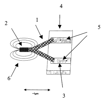
Figure 1 shows a schematic drawing of an analytical device for use in a
nanoscale
MRFM containing the CNT cantilever probe of the invention.
6
CA 02499370 2005-03-17
WO 2004/038430 PCT/US2003/029520
Figure 2 shows a schematic drawing of an MRFM layout of the analytical device
with a
CNT cantilever probe.
Figure 3 shows scanning electron microscope (SEM) photomicrographs of
symmetrically
branched (Y-shaped) CNTs at (a) low magnification (scale bar = 1 Vim) and (b)
high
magnification (scale bar = 200 nm).
Figure 4a shows an SEM image of about 100 nm diameter mufti-walled CNTs grown
by
a CVD process on nanolithographically prepared silicon substrates.
Figure 4b shows an AFM photomicrograph of tungsten wires on silicon-nitride on
a
silicon wafer surface.
DETAILED DESCRIPTION OF THE INVENTION
Defiyaitio~as
The term "CVD" refers to chemical vapor deposition. In CVD, gaseous mixtures
of
chemicals are dissociated at high temperature (for example, COa into C and
OZ). This is the
"CV" part of CVD. Some of the liberated molecules can then be deposited on a
nearby substrate
(the ''D" in CVD), with the rest pumped away.
The term "piezoresistance" is defined in the art as a change in resistance in
a material,
caused by an applied stress. Piezoresistance or piezoelectric properties of
CNTs are the
variations of the electrical resistance of the CNT due to stress caused by a
deflection or bending
of at least one end.
The term "ferromagnetic" is afforded the term commonly given in the art. A
"ferromagnetic material" is a material having the ability to maintain
magnetization in the
absence of a magnetic field. Typical ferromagnetic materials comprise elements
selected from
transition metals of the periodic table and alloys thereof. Preferred
ferromagnetic elements are
cobalt, iron, nicl~el, and alloys thereof.
The term "nanomagnet" is defined in the art as a ferromagnetic material having
dimensions from about 1 nanorneter (nm) to about 10 micrometers.
7
CA 02499370 2005-03-17
WO 2004/038430 PCT/US2003/029520
MRFM device comprising a CNT fe~~omaghetic probe
The present invention provides an MRFM analytical device comprising a micro-
dimensional probe that is capable of detecting single proton and single
electron spin. In
particular, the present invention provides a micro-dimensional probe for an
MRFM device that
comprises a CNT cantilever that includes a ferromagnetic particle. The CNT
cantilever can be
attached to an electrode as a component of a probe. The probe can be coupled
with an electrical
circuit as a component of a device for nanoscale MRFM micro-dimensional
probes.
Figure 1 depicts a device of the present invention. Two arms of a branched CNT
cantilever 1, are connected to electrodes 3, which are on the surface of
substrate 4. A
ferromagnetic material 2 is attached to the cantilevered end of CNT cantilever
1. Arrows 5 show
the direction of an alternating electrical current flowing thought the device.
The gradient field
felt by the specimen spins are represented by dashes lines 6.
CNTs are cylinders of networked carbon atoms that can have cylinder diameters
as small
as about 0.4 nm (1 nm = 10-9 m). CNTs can be prepared in typical lengths from
about 10 nm to
about 100,000 nm (0.1 mm) and diameters from about 1 nm and about 100 nm. The
smallest
diameter CNTs (about 0.4 nm to about 10 nm, typically) are comprised of a
single tubule of
networked carbon atoms, and are referred to as single-walled carbon nanotubes
(hereinafter
referred to as SWNTs). CNTs also appear as nested concentric cylinders,
referred to as
multiwalled carbon nanotubes (hereinafter referred to as MWNTs). For the
present invention,
preferred dimensions are diameters between about 1 nm and about 50 nm, and
lengths between
about submicron and about 100 micrometers. In a currently preferred
embodiment, the CNT
tubules have a length ranging between about 1 micrometer to about 10
micrometers. CNTs have
conducting properties depending on chirality (the rotation of the symmetry of
carbon network
along the cylinder axis). CNTs can be metallic, semiconducting or insulating.
Single walled
nanotubes can be metallic or semiconducting, depending on chirality, while
MWNTs are
observed to be only metallic, likely a result of mixed chirality among the
carbon layers. Both
CNT species are mechanically robust, with a Young's modulus of about 1 TPa
(1012 Pa).
The sub-micron diameter malces CNTs ideal candidates for the reduced-size,
"nanoscale"
cantilevers required for MRFM imaging of nanoscale features in samples.
Moreover, the small
dimensions will lead to increased mechanical resonance frequencies due to the
smaller mass
(resonance frequency varies inversely with the square root of the mass fo ~
lhnl~2), a beneficial
8
CA 02499370 2005-03-17
WO 2004/038430 PCT/US2003/029520
quality for imaging. CNTs offer significant advantages in that they possess
piezoelectric
properties. The piezoelectric properties allows the means of internally
detecting the movement
of a cantilever comprised of a CNT. The means of internally detecting movement
eliminates the
need for an external detection such as the reflection of a laser beam off the
cantilever toward a
photodiode detector. CNTs also possess substantially higher strength-to-weight
ratio and
superior mechanical properties over other materials such as silicon.
CNTs can be linear or non-linear. "Linear CNTs" as defined herein, refer to
CNTs that
do not contain any branches originating from the surface of individual CNT
tubules along their
linear axes. "Branched CNTs" as defined herein, refer to non-linear CNTs with
at least one
location along the linear tubule axis or at the tubule terminal from which one
or more tubules
originate, having linear tubule axes that are non-identical to the tubule from
which they originate.
Such points of origination of additional tubules (branch points) are also
referred to herein as
"junctions". Branched CNTs include, for example, "Y-shaped" CNTs and "V-
shaped" CNTs.
The individual arms constituting branched tubules are either symmetrical or
unsymmetrical with
respect to both arm lengths and the angle between adjacent arms. In one
embodiment, the
individual arms are between about 1 nm and about 100 micrometers in length.
Figure 3 shows
example images of Y-shaped CNTs. In one embodiment of the present invention,
the probe
comprises a CNT which is Y-shaped. The Y-shaped CNTs exist as (1) a plurality
of free
standing, branched CNTs attached to the substrate and extending outwardly from
the substrate
outer surface; and (2) one or more CNTs with a branched morphology wherein the
CNT tubule
structures have Y junctions with nominally straight tubular arms and nominally
fixed angles
between said arms. In another embodiment of the present invention, the probe
comprises a CNT
cantilever which is, V-shaped. Figure 4a shows images of V-shaped CNTs.
Tinportant stmctural
attributes of CNTs that determine their mechanical and electrical properties
can be controlled
and "tailored" for specific requirements.
The ferromagnetic particle of the present invention comprises a ferromagnetic
material.
Typical ferromagnetic materials comprise elements selected from transition
metals of the
periodic table and alloys thereof. Preferred ferromagnetic elements are
cobalt, iron, nickel, and
alloys thereof. In one embodiment, the ferromagnetic particle is in the form
of a nanorod, with
preferred length about 10 nm to about 100 nm, axld preferred length to
diameter ratio of about ~
to about 100.
9
CA 02499370 2005-03-17
WO 2004/038430 PCT/US2003/029520
The invention provides methods for fabricating an analytical device comprising
a CNT
cantilever probe. Figures 1 and 2 show the assembly of the components
comprised in the
MRFM analytical device. For an MRFM application, the nanotube is positioned as
follows: ,
immobilizing two arms of a Y to two electrodes on a substrate, with the third
arm cantilevered
out from the substrate edge, as depicted in Figures 1 and 2. Figure 2 depicts
the full MRFM
layout of the device in which the CNT cantilever 1 is cantilevered out from
the substrate 3, and a
ferromagnetic material 2 is attached to the free arm of the CNT cantilever 1.
The gradient field 6
is felt by sample spins 5. An RF coil is represented as a microcoil 4
integrated into the substrate
3 and produces an RF magnetic field 7.
Branched CNT cantilevers are attached to or grown onto lithographically
prepared
substrates containing surface metal electrodes. In a preferred embodiment, the
substrate
comprises on-chip signal processing capabilities.
The Y-shaped CNTs are used as an MRFM cantilever by attaching the ends of the
top
two arms of the Y to a substrate, with the bottom, third arm cantilevered out
over the edge of the
substrate. Examples of Y-shaped carbon nanotube are shown in Figure 3.
The V-shaped CNTs are used as an MRFM cantilever by attaching the arms of the
V to a
substrate, with the junction cantilevered out over the edge of the substrate.
Examples of V-
shaped carbon nanotube are shown in Figure 4a.
Y-shaped and V-shaped CNTs are placed on a substrate using Scanning Probe
Microscopy (SPM) manipulation techniques which are known in the art. They can
be situated to
protrude perpendicularly from the substrate, or can lie parallel to the
substrate at a substrate
edge, such that the device cantilevers out from the edge.
Connection of the CNT cantilever to a substrate, such as for example silicon,
may be
accomplished in the following ways: namely, device-on-electrodes, and
electrodes-on-device. In
the former, device-on-electrodes configuration, metallic lead electrodes are
deposited by
conventional lithographic techniques, possibly including electron-beam
lithography, onto a
passivated semiconductor substrate (e.g. silicon dioxide or silicon nitride,
on silicon). These
electrodes are of appropriate thiclcness, width, length and proximity for
later attachment of CNT
cantilevers. In one aspect, preferred electrode dimensions are thickness of
about 100 nm, width
CA 02499370 2005-03-17
WO 2004/038430 PCT/US2003/029520
of about 100 nm, length of up to several millimeters (in one embodiment,
length of about 1 mm),
and proximity (distance between two planar electrodes) of about 100 nm. The
substrate may be
prepared with vertical void regions, or edges, with the above electrodes
deposited to the edges.
CNT cantilevers may then be placed onto the substrate, such as by dispersion
of CNTs in
solution which is then evaporated, and physically manipulated into place atop
the prepared
electrodes. One end of a "Y" or the joint of the "V" would be cantilevered out
over the substrate
edge, or over the void area, forming a cantilever. Additional electrical
contact of the fixed ends
of the "V" or "Y" CNT to the surface metallic electrodes could be achieved by
electrodeposition,
electroless deposition, or electron beam "welding" in a scanning electron
microscope (SEM).
For the latter electrodes-on-device configuration, the CNT cantilever is
situated on the
substrate prior to metal electrode deposition. In a similar fashion to the
former device-on-
electrodes configuration, the CNT is manipulated with an SPM into position,
forming a
cantilever. The planar coordinates of the final location of the CNT can be
identified with an
SEM or an SPM. These coordinates are then later used to program a
photolithographic or
electron beam lithographic system to accurately place metallic electrodes onto
a surface and
overlapping the ends of the fixed portions of the CNTs, making electrical
contact. Another
aspect of preparation of the electrodes-on-device configuration involves a Y
or V-shaped CNT
situated flat on a substrate. Photolithographic techniques known to the art
are then used to both
accurately place metallic electrodes overlapping the ends of the Y or V-shaped
CNT, a~ld to etch
the substrate so as to remove substrate material below a portion of the CNT,
facilitating a
cantilevered arrangement.
An advantage of using V-shaped CNTs is the ability to grow the CNT cantilevers
directly
on the substrate, Without the added step of attaching a pre-formed CNT
cantilever to the
substrate. V-shaped carbon nanotube devices can be formed by growing two
nanotubes in
precise, close proximity (typically from about 10 nm to about 100 nm) using
nanoscale electron-
beam lithography, and attaching a ferromagnetic particle to their juncture.
Figure 7 shows an AFM image of tungsten wires on silicon-nitride on a silicon
wafer
surface. The bumps visible at the ends of each wire are nickel nanodots
situated to serve as
catalyst sites for subsequent growth of CNTs. Referring to Figures 4a and 4b,
closely spaced
nanotubes can be brought into contact electrostatically, and then attaching,
by for example
electroless deposition, a ferromagnetic nanopaxticle to their juncture. The
resulting V-shaped
11
CA 02499370 2005-03-17
WO 2004/038430 PCT/US2003/029520
device can then be excited electromagnetically (Lorentz force) into mechanical
resonance, for
MRFM detection.
Nanofnagnetic Incorporated CNT Pf~obes
CNTs' with pre-determined morphology, such as for example, Y-shaped CNTs, can
be
synthesized using a variety of methods known in the art. Preferred processes
for producing
quantities of CNTs having varied morphology, including Y-shaped CNTs, are
described in W. Z.
Li, et al. Applied Physics Letters, Volume 79 (12), 2001, Pages 1879-1881, and
J. Li, et al.
Applied Physics Letters, Volume 75 (3), 1999, Pages 367-369, which are
incorporated herein by
reference in their entirety.
As shown in Figure 3, branched CNTs typically comprise a plurality of Y
junctions with
substantially straight arms extending linearly from said junctions. The
majority of branched
CNTs possess Y junctions having two long arms that are a few microns long
(about 2 to about
10 Vim), and a third arm that is shorter (about 0.01 to about 2 ~,m). CNTs
with Y junctions
comprising three long arms (up to about 10 Vim), and with multiple branching
forming multiple
Y junctions with substantially linear, straight arms can be also obtained by
the method of the
invention. A high magnification SEM micrograph (Figure 3b) shows that branched
CNTs
typically possess Y junctions that have a smooth surface and uniform tubule
diameter about
200 nm. The angles between adjacent arms are close to about 120°,
thereby resulting in
branched CNTs that have a substantially symmetric structure. All Y junctions
have a
substantially similar structural configuration, regardless of their varying
tubule diameters.
The CNTs comprised in the probes of the present invention can be synthesized
in
addressable arrays. Fabrication of addressable CNT arrays utilizes both micro-
and nano-
lithographic preparation of CNT catalyst sites and metallic addressing wires
on single crystal
silicon wafers. Subsequently, growth of aligned CNTs on the catalyst surface
is accomplished
via CVD. Essentially, a series of thin gold wires are defined lithographically
on the surface of
the silicon wafer, wherein the inner ends of pairs of individual wires are in
close proximity, for
example, about 100 nm. A CNT growth catalyst (for example, nickel (Ni) or
cobalt (Co))
nanodot site is defined at these proximal ends using e-beam lithography,
following which the
catalyst material is deposited. The wafers axe then placed in a chemical vapor
deposition (CVD)
chamber to initiate CNT growth. CNT growth occurs only at the catalyst
nucleation sites.
12
CA 02499370 2005-03-17
WO 2004/038430 PCT/US2003/029520
The fabrication schemes for MRFM probes of the present invention rely on the
use of a
nanomagnet such as a ferromagnetic material as the field sensor. In one
embodiment a
ferromagnetic material can be attached to the branched CNT cantilever of the
present invention
post-synthesis using typical deposition techniques lcnown in the art (e.g.,
CVD, and electroless
deposition). hz another embodiment, the ferromagnetic material is incorporated
onto the CNT
cantilever as a result of in situ nanotube formation.
In one aspect, the nanomagnet material in the tubule ends of the CNT
cantilever probes
of the present invention are generated in-situ during the CNT synthesis. In
one embodiment, the
catalytic material used in the tubule synthesis comprises a ferromagnetic
material that is retained
at the tubule ends of the branched CNTs upon synthesis, thereby functioning as
"in-situ
deposited" nanomagnets in the CNT probe of the invention. Preferred metal
catalysts include the
metallic materials, including their mixtures and alloys that have
ferromagnetic properties.
Preferred transition metals include iron, cobalt and nickel, including
mixtures and alloys thereof.
In a currently preferred embodiment, the transition metal is cobalt. For the
in-situ incorporation
of the nanomagnet material on the CNT probes of the invention, the catalytic
material
comprising at least one transition metal or transition metal alloy that is
deposited on or
impregnated within a support substrate comprising a metallic material or a non-
metallic material,
such as for example, a non-metallic oxide as microparticles. The catalyst
micropaxticles
nucleate the tubule growth in the CNT growth process, whereby they migrate
towards the
growing ends of the branched CNT tubules and aggregate to form a nanomagnet.
The non-
metallic oxide comprising the catalytic substrate can be either a transition
or a non-transition
metallic oxide, or a non-metallic inorganic oxide. Metallic oxides useful in
the catalyst materials
include, for example, oxides of beryllium, magnesium, calcium, strontium and
barium. Preferred
metallic oxides include magnesium oxide and calcium oxide. In a currently
preferred
embodiment, the metallic oxide is magnesium oxide (Mg0). The CNT growth
process can be
controlled to obtain tubules of approximately uniform dimensions within
arrays. Depending on
growth conditions (which in turn, are influenced by the catalyst material),
individual tubules in
an array can vary in height between about 10% to about 50% in any given growth
run. Important
parameters in the growth process of the CNT probe component of the present
invention can be
varied to include the separation distance between catalytic sites on the
substrate (and therefore,
between tubule pairs, and tubule branches), and the dimension (diameter and
height) of the
catalyst microparticles that nucleates the tubule growth and the catalyst
deposition method
thereby providing control over the size of the nanomagnet growth in situ.
Control of the CNT
13
CA 02499370 2005-03-17
WO 2004/038430 PCT/US2003/029520
growth process can be utilized to obtain CNT probes of the invention
comprising in-situ
generated nanomagnets and mufti-walled CNTs with tubule diameters that are
controllable down
to about 100 nm. CNT probes with smaller tubule sizes can be obtained by using
aligned CNT
arrays of single-walled nanotubes.
The nanotube structure can be driven into mechanical resonance with a Lorentz
force,
obtained with the use of a static polarizing field oriented in the plane of
the "Y" or "V", crossed
by an alternating current passing through the two anchored arms of the
structure, as in Figure 2.
A ferromagnetic material fixed to the CNT cantilever serves as both the
generator of a strong
magnetic field gradient to be felt by the spin system to be analyzed (see, for
example, Figure 2),
and as the active magnetic sensor which feels the reaction force applied by
this spin system. In
the usual SPM manner, this MRFM detector can be x-y-z scanned to facilitate 3D
imaging of the
sample.
The two fixed arms of the branched CNT cantilever may be attached to metallic
electrodes, and an electric current can be sent into one arm and out the
other, as in Figure 1. As
the cantilevered end of the branched assembly moves under the influence of
magnetic forces, a
strain-induced change in the electrical resistance of the assembly is
measured.
The special shape of the branched CNT structures facilitates direct electrical
resistance
measurements, with nanotube cantilever deflection causing resistance changes
via the
piezoresistance effect, measured through the two attached arms of the branched
CNT cantilever.
The conducting, and piezoconducting, properties of these mufti-walled CNTs are
sensitive to defects, over which there is some degree of control in the
growing stage. The defect
sensitivity can be beneficial. In addition to piezoresistance, the branched
CNT can exhibit
nonlinear rectifying characteristics, such as for example, in a diode, such
that the strain
dependent conductivity of the nanotube can be incorporated into a nanoscale
amplifying circuit
such as for example, a FET, dramatically enhancing the sensitivity to motion.
Diodic behavior at
room temperature is observed by both STM studies and direct transport across
large arrays.
Thus, in addition to using piezoresistance to detect the branched CNT
cantilever motion, a
related detection method could integrate the structure into a nanoelectronic
transistor circuit,
with potential for significant gains in sensitivity.
The present invention has several advantages. The invention directly overcomes
one of
the main disadvantages to observation at the molecular level using
cantilevers, that of output
14
CA 02499370 2005-03-17
WO 2004/038430 PCT/US2003/029520
signal. The method of the present invention uses piezoelectric detection with
CNT cantilevers,
thereby eliminating the need for laser interferometry mirrored-light detection
as required by
silicon-based cantilevers. CNTs are lcnown in the art to be high strength,
mechanically robust,
flexible conducting materials. The use of CNTs as cantilevers in place of
silicon-based
cantilevers in MRFM, improves the state-of the-art technology from micrometer-
scale resolution
by orders of magnitude to nanometer-scale resolution. Nanotubes improve
sensitivity and spatial
resolution up to about 1,000 times more than possible with silicon-based
cantilevers. CNT
cantilevers are compatible with conventional technologies for fabricating
electrically conducting
nanocircuits, such as etched trenches in silicon or surface deposition of
thick nanowire contacts.
Nanotube cantilevers can be used in inconvenient environments such as
biological media. The
disclosed devices have the capability of being built in array form, allowing
real-time, correlative
spectroscopy and imaging. Spatially and temporally correlated detection, in
the spirit of
functional MRI are possible. The present invention is a unique and enabling
technology that has
the revolutionary capability to fabricate arrays of ultra-sensitive MRFM
devises that can be used
for fast imaging. The present invention advances the measurement capabilities
of magnetic
detection by reducing the size of the measurement tools to the nanoscale.
Instead of
micromachining silicon down to the appropriate size, the present invention
uses CNTs.
The present invention provides new technologies for constructing MRFM
instruments
that outperform the current generation of MRFM instruments by several orders
of magnitude in
sensitivity and resolution. CNTs will enable three-dimensional magnetic
resonance imaging of
samples such as single impurities in solids, biological cells and biological
molecules such as
DNA at the molecular level.
The devices of the invention, including mechanical and chemical processes for
their
preparation, as well as methods for their fabrication will become apparent to
one familiar in the
art based on the aforementioned embodiments and the following non-limiting
examples.
EXAMPLES
Example 1.
Preparation of catalyst substrate for synthesis of linear CNTs
Mesoporous silica containing iron nanoparticles were prepared by a sol-gel
process by
hydrolysis of tetraethoxysilane (TEOS) in the presence of iron nitrate in
aqueous solution
CA 02499370 2005-03-17
WO 2004/038430 PCT/US2003/029520
following the method described by Li et al. (Science, (1996), Yol. 274, 1701-
3) with the
following modification. The catalyst gel was dried to remove excess water and
solvents and
calcined for 10 hours at 450°C and 10'2 torr to give a silica network
with substantially uniform
pores containing iron oxide nanoparticles that are distributed within. The
catalyst gel is then
ground into a fine, micro-particulate powder either mechanically using a ball
mill or manually
with a pestle and mortar. The ground catalyst particles provide particle sizes
that range between
0.1 and 100 ~M under the grinding conditions.
Example 2.
Preparation of catalyst substrate for synthesis of branched CNTs
Catalyst substrates were prepared following the method described by Li et al.
(Applied
Physics Letters (2001) Yol. 79(12), I X79-1881). Magnesium oxide (Mg0)
supported cobalt (Co)
catalysts were prepared by dissolving 0.246 g of cobalt nitrate hexahydrate
(Co(N03)2.6H2O,
98%) in 40 ml ethyl alcohol, following immersing 2 g of particulate Mg0 powder
(-325 mesh)
were added to the solution with sonication for 50 minutes. The solid residue
was filtered, dried
and calcined at 130°C for 14 hours.
Example 3.
General synthetic procedure for branched CNTs
The Mg0 supported cobalt catalyst of Example 2 were first reduced at
1000°C for 1 hour
in a pyrolytic chamber under a flow of a mixture hydrogen (40 sccm) and
nitrogen (100 scan) at
a pressure of 200 Torr. The nitrogen gas was subsequently replaced with
methane (10 sccm) to
initiate CNT growth. The optimum reaction time for producing branched CNTs was
1 hour.
Example 4.
Characterization of CNT morphology and purity by Scanning Electron Microscopy
(SEM),
and tubule structure and diameter by Transmission Electron Microscopy (TEM)
Scanning electron microscopy (SEM) for characterization and verification of
CNT
morphology and purity was performed on a JEOL JSM-6340F spectrophotometer that
was
equipped with an energy dispersive x-ray (EDS) accessory. Standard sample
preparation and
analytical methods were used for the SEM characterization using a JEOL JSM-
6340F
16
CA 02499370 2005-03-17
WO 2004/038430 PCT/US2003/029520
microscope. SEM micrographs of appropriate magnification were obtained to
verify tubule
morphology, distribution and purity.
Transmission electron microscopy (TEM) to characterize individual tubule
structure and
diameter of the CNTs was performed on a JEOL 2010 TEM microscope. Sample
specimens for
TEM analysis were prepared by mild grinding the CNTs in anhydrous ethanol. A
few drops of
the ground suspension Were placed on a micro-grid covered with a perforated
carbon thin film.
Analysis was carried out on a JEOL 2010 microscope. TEM micrographs of
appropriate
magnification were obtained for determination of tubule structure and
diameter.
Example 5.
Controllable creation of arrays of addressable mufti-walled carbon nanotubes
CNTs are grown by the plasma-enhanced hot filament chemical vapor deposition
method, including on an e-beam patterned substrate. Metallic nickel, deposited
via e-beam
lithography over a non-catalytic metal provides the electrical leads, is used
as the catalyst for
CNT growth.
Example 6.
Microdimensional electrically addressable probe fabrication
Catalyst deposition ott substt~ate
The preliminary step in probe fabrication involves a micro- and
nanolithographic
preparation of CNT catalyst sites and metallic addressing wires on single
crystal silicon wafers.
Conventional e-beam evaporation of nickel (Ni) or cobalt (Co) is used after an
e-beam
lithography step is performed on the substrate to define the catalyst sites in
an e-beam resist.
This is followed by a lift-off step (of the unwanted catalyst material),
leaving only the Ni or Co
nanodots on top of the gold leads. Alternatively, a self assembly of catalyst
nano-particles from
a catalyst-containing solution is used, which precludes the need for the lift-
off step. In either
case, at the end of this phase, electrically addressable pairs of CNTs with
well-defined heights
and lateral separations are prepared. Separations between nanotubes down to 10
nm, can be
obtained reproducibly by these methods.
17
CA 02499370 2005-03-17
WO 2004/038430 PCT/US2003/029520
Faby~ication of electYically-addYessable carbon raanotube a~~ays
An array of aligned CNTs are grown on the substrate containing catalytic sites
via hot
filament, plasma-enhanced chemical vapor deposition (PECVD). A series of thin
gold wires
lithographically on the silicon is defined, with the inner ends of pairs of
individual wires in very
close proximity (about 100 nm). At these proximal ends, a CNT growth catalyst
(for example,
Ni or Co) nanodot site is defined using e-beam lithography, and the catalyst
material deposited.
This wafer is then placed in the CVD chamber, with subsequent CNT growth
occurring only at
the catalyst nucleation sites. At this point the gold wires may be passivated
using
electropolymerization. If deemed necessary, additional steps can be introduced
to obtain strictly
uniform height of the CNTs in the arrays. Depending on growth conditions used,
CNTs height
in an array in a given growth run can be varied in height by 10%-50%. Height
uniformity is
accomplished by performing additional mechanical polish steps.
All patents, patent applications, and published references cited herein are
hereby
incorporated by reference in their entirety. While this invention has been
particularly shown and
described with references to preferred embodiments thereof, it will be
understood by those
skilled in the art that various changes in form and details may be made
therein without departing
from the scope of the invention encompassed by the appended claims.
18