Note: Descriptions are shown in the official language in which they were submitted.
CA 02499842 2005-03-22
WO 2004/030749 PCT/US2003/030568
-1-
APPA RATUS AND METHOD FOR OPTIMIZING CAPACITOR CHARGE IN
A MEDICAL DEVICE
This application relates to the following concurrently filed, commonly
assigned
U.S. patent application: "Method and Apparatus for Maintaining Energy Storage
in an
Electrical Storage Device", reference number P-9171.00 filed September 30,
2002,
which is incorporated herein by reference.
The present invention relates generally to stimulators for medical treatment
by
means of voltage shocks, and more particularly to cardioverters and
defibrillators and
electrode systems for use in conjunction therewith.
A defibrillator can be used to restore a normal heart rhythm by delivering an
electrical shock to the heart when the heartbeat is dangerously fast due to
ventricular
tachycardia or ventricular ribrillation. Either of these conditions can reach
a life-
threatening point at which a pexson suddenly loses consciousness because the
heart can
no longer pump enough blood to meet the body's demand. For patients suffering
from
chronic arrhythmias involving ventricular tachycardia or ventricular
fibrillation, a
defibrillator can be surgically implanted in the patient's chest. The
implanted
defibrillator can be implanted into the chest of the patient during a minor
surgical
procedure.
An implantable cardioverter defibrillator (ICD) is a device that can be
implanted in
a patient's chest to monitor for and, if necessary, correct episodes of rapid
heartbeat.
If the heartbeat gets too fast (ventricular tachycardia), the ICD can
stimulate the heart
to restore a normal rhythm. In cases where the heartbeat is so rapid that the
heart
cannot effectively pump any blood (ventriculax fibrillation), the ICD can
provide an
electric shock to "reset" the heartbeat.
The ICD gets its name from the two functions that it performs. First, the ICD
sends small electrical charges to the heart to "reset" it during ventricular
tachycardia.
This process of converting one rhythm or electrical pattern to another is
called
CA 02499842 2005-03-22
WO 2004/030749 PCT/US2003/030568
-2-
cardioversion. Second, the ICD will send stronger charges to "reset" the heart
if it
begins ventricular fibrillation instead of beating. The act of stopping this
potentially
fatal quivering of the heart is called defibrillation. Although the main
functions of the
ICD are cardioversion and defibrillation, it can also be programmed to do anti-
tachycardia and bradycardia pacing.
In anti-tachycardia pacing, when an ICD senses a fast but rhythmic heartbeat
(tachycardia), it can release a series of low-intensity electrical pulses that
gently
interrupt the heart and allow it to return to a slower pace. In bradycardia
pacing, when
the ICD senses an abnormally slow heartbeat, it can send small electrical
signals to
pace the heart until it recovers and maintains a normal heart rate. These
therapies are
contrasted with both cardioversion and defibrillation, which involve high
voltage
shocks, which is the focus of the present invention.
In all of the ICD systems available today, a truncated capacitive-discharge
shock is
delivered by the ICD to electrodes that are positioned in, on, or near the
heart. To
generate the shock, existing ICD systems use an internal high current
electrical battery
cell connected to a step-up transformer and power conversion cixcuitry to
charge one
or more relatively small, but powerful, high voltage capacitors to provide a
relatively
high discharge voltage. When an electrical stimulation pulse is to be applied
to the
heart, the appropriate output switch is closed to connect the output capacitor
to the
cardiac tissue through the electrodes, thereby effectively "dumping" the
charge stored
in the output capacitor into the cardiac tissue. After the output decays to a
predetermined output voltage, or after a predetermined shock duration has
elapsed, the
shock is truncated and the remaining energy in the output capacitor system is
dissipated within the ICD system never being utilized or recovered.
The primary function of an ICD is to sense the occurrence of an arrhythmia,
and to
automatically apply an appropriate shock therapy to the heart aimed at
terminating the
arrhythmia. For example, if the ICD senses that the patient's heart is
fibrillating then
the ICD automatically delivers a high current shock to the patient's heart to
defibrillate
the organ. ICDs typically operate by first detecting the arrhythmia, then
rapidly
charging one or more storage capacitors contained within the device, and then
quickly
CA 02499842 2005-03-22
WO 2004/030749 PCT/US2003/030568
-3-
discharging the capacitors) to deliver the life saving shock therapy. However,
a
problem associated with rapidly charging a capacitor is that it creates a
severe load on
the battery. Thus reducing the battery's life.
An additional problem associated with the high voltage capacitors of an ICD is
the
amount of time it takes to charge the capacitors, typically about 5 to 20
seconds,
Many studies have proposed that defibrillation and cardioversion shocks are
most
effective when delivered as quickly as possible following detection of
arrhythmia. The
chance of terminating an arrhythmia in a patient decreases as the length of
time it takes
for therapy to be delivered to the patient increases. Therefore, the shorter
the charge
time for the capacitors the more effective the defibrillation therapy.
Typically, ICD
battery sizes are proportional to the charging time. Therefore, the quicker
the desired
charging time, the larger the battery. In spite of this, it is desirable to
make the ICD as
small as possible and therefore large batteries are not desired and thus a
balance must
be struck between having a fast charging time and the size of the ICD.
Another problem involves providing a capacitor that maintains a high
capacitance
while at the same time has a reduced leakage current. The term "leakage
current"
refers to the measure of stray direct current flowing through a capacitor
after DC
voltage is impressed on it and is expressed in milliamps. The dielectric of a
capacitor
has a very high resistance, which prevents the flow of DC current. However
there are
some areas in the dielectric, which allow a small amount of current to pass.
The value
of leakage current will continue to decrease while voltage is applied to the
capacitor,
until a very low steady state leakage current value is reached. However, as
stated
above, the present ICDs allow the remaining capacitor charge to dissipate
after the
arrhythmia has been treated. The longer capacitors are stored with no applied
voltage,
the higher the initial leakage current. Therefore, the constant recharging and
the length
between the recharging of the capacitors actually increases the amount of
leakage
current. A high leakage current can result in the poor performance and
reliability of a
capacitor. In particular, high leakage current results in a greater amount of
charge
leaking out of the capacitor once it has been charged. This is undesirable.
CA 02499842 2005-03-22
WO 2004/030749 PCT/US2003/030568
-4-
Another problem associated with the present ICDs, is that the remaining charge
after the arrhythmia is treated is just dissipated within the ICD. While the
charge
dissipated is relatively minimal when compared to the shock charge, after
hundreds of
shocks the remaining charges can add up to a substantial shock. Typically, 16
remaining charges can add up to provide a defibrillation shock. Further, the
dissipated
remaining charges equate to energy taken from the battery and never put to
use.
Therefore, it would be desirable to capture these remaining charges and thus
extend
the Iife of the battery.
For the foregoing reasons, there is a need for an ICD, which allows for a
relatively
long charging time and yet retains clinical efficacy to prolong battery life
and provide
for a smaller battery. There is also a need for an ICD providing a high
voltage
capacitor with very low leakage current so that the capacitor could be held at
full
charge thus reducing the adverse effects of rapid charging. There is also a
need for an
ICD that when an arrhythmia is detected the ICD can deliver therapy at the
quickest
possible moment without having to wait for a capacitor to charge thus
increasing the
efficacy of the delivered therapy.
A medical device for electrical termination of an arrhythmic condition of a
patient's heart in embodiments of the invention may include one or more of the
following features: (a) at Ieast one battery; (b) means for detection of an
arrhythmic
condition of a patient's heart; (c) at least one high voltage capacitor; (d)
converter
means for providing charging current from said at least one battery to said at
least one
capacitor; (e) means for maintenance of a charge on said at least one
capacitor between
arrhythmia therapies; (f) controller means responsive to detection of an
arrhythmic
condition of said patient's heart and for providing a discharge control
signal; and (g)
discharge circuit means for delivering voltage stored on said capacitor to
said patient's
heart in response to said discharge control signal.
A method for electrical termination of an arrhythmic condition of a patient's
heart
in embodiments of the invention may include one or more of the following
features:
(a) charging at Ieast one high voltage capacitor with current from at least
one battery,
(b) detecting an arrhythmic condition of a patient's heart, (c) maintaining
the charge
CA 02499842 2005-03-22
WO 2004/030749 PCT/US2003/030568
-5-
on said at least one capacitor between arrhythmia therapies, (d) providing a
controller
means responsive to detection of an arrhythmic condition of said patient's
heart, (e)
generating a discharge control signal upon detection of an arrhythmic
condition of said
patient's heart; and (f) delivering a voltage stored on said capacitor to said
patient's
heart in response to said discharge control signal.
FIG. 1 is a drawing illustrating the general physical components of a
pacemaker/cardioverter/defibrillator and lead system of the type in which the
present
invention may be advantageously practiced;
FIG. 2 is a functional block diagram illustrating the general interconnection
of
voltage conversion circuitry of the present invention with the primary
functional
components of an implantable pacemaker/cardioverter/defibrillator;
FIG. 3 is a schematic block diagram of the general components of a
pacemaker/cardioverter/defibrillator employing a high voltage charging
circuit;
FIG. 4 is a flow diagram of an embodiment for capacitor optimization of the
present invention;
FIG. 5 is a table representing a capacitor optimization embodiment of the
present
invention;
FIG. 6 is a flow diagram of an embodiment for capacitor optimization of the
present invention;
The following detailed description is to be read with reference to the
figures, in
which like elements in different figures have like reference numerals. The
figures,
which are not necessarily to scale, depict selected embodiments and are not
intended to
limit the scope of the invention. Skilled artisans will recognize that the
examples
provided herein have many useful alternatives that fall within the scope of
the
invention.
The pxesent invention is not limited to implantable cardioverter
defibrillators and
may be employed in many various types of electronic and mechanical devices for
CA 02499842 2005-03-22
WO 2004/030749 PCT/US2003/030568
-6-
treating patient medical conditions such as external cardioverter
defibrillators,
pacemakers, and neurostimulators. It is to be further understood; moreover,
the
present invention is not limited to medium current rate batteries and may be
utilized
for low and high current rate batteries. For purposes of illustration only,
however, the
present invention is below described in the context of medium current rate
batteries
and implantable cardioverter defibrillators.
The present invention is described generally in a system providing biphasic
cardioversion pulses or shocks in a cardioversion system. However, it is fully
contemplated that the present invention could be utilized in any type of pulse
or shock
delivery methodology utilizing any type of pulse of shock waveform without
departing
from the spirit of the invention. In the description of the preferred
embodiment that
follows, an implantable pacemaker/cardioverter/defibrillator in which the
present
invention is preferably implemented is capable of providing monophasic,
biphasic, or
any other caxdioversion pulse or shock waveform. However, a variety of
implantable
leads and electrode systems may be employed, with more than one cardioversion
electrode connected electrically in common to widen the cardioversion energy
distribution across the heart. Such electrodes may include indwelling right
ventricular,
superior vena cava, and coronary sinus electrodes, active pulse generator case
electrodes and/or epicardial and subcutaneous patch electrodes in various
combinations of two or more. With a three electrode system, two of the
electrodes are
connected in common, and the energy distribution between the two common and
the
third electrode may lead to reduced energy sufficient to reliably cardiovert a
heart in
fibrillation or high rate malignant ventricular tachycardia.
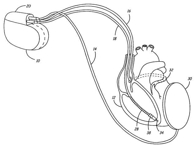
FIG. 1 illustrates such a general implementation of an implantable
pacemaker/cardioverter/defibrillator 10 and one possible selection of
cardioversion
electrodes on associated electrical leads 14, 16 and 18, and their
relationship to a
human heart 12. The leads 14, 16, and 18 are coupled to the
pacemaker/cardioverter/defibrillator 10 by means of a mufti-port connector
block 20,
which contains separate connector ports fox each of the three leads
illustrated. Each of
the leads 14, 16, 18 comprise a large surface area cardioversion electrode,
and lead 18
CA 02499842 2005-03-22
WO 2004/030749 PCT/US2003/030568
_7_
also comprises a pair of pace/sense electrodes (making it a tripolar lead) all
as
described below.
Unipolar lead 14 is coupled to a subcutaneous cardioversion electrode 30,
which is
intended to be mounted subcutaneously in the region of the left chest.
Unipolar lead
16 is a coronary sinus (CS) lead employing an elongated coil, cardiovexsion
electrode
that is located in the coronary sinus of the heart. When positioned in the CS,
the CS
electrode extends around the heart from a point within the opening or ostium
of the CS
to a point in the vicinity of the left atrial appendage, as shown in broken
line format at
32.
Tripolar lead 18 is provided with an elongated electrode coil 28 which is
located in
the right ventricle of the heart and functions as a third cardioversion
electrode. Lead
18 also includes a first pace/sense electrode 34 and a second, closely spaced,
pace/sense electrode 38. Electrode 34 takes the form of a distal helical coil,
which is
screwed into the myocardial tissue of the right ventricle. The second
pace/sense
electrode 38 is closely spaced to the electrode 34 for bipolar pacing and near
fteld
electrogram or R-wave sensing in the apex of the right ventricle. A more
detailed
description of the leads illustrated can be found in U.S. Pat. No. 5,163,427,
herein
incorporated by reference in its entirety.
Through testing at implantation of cardioversion efficacy across one of the
three
electrodes with the other two electrodes in common or with each of the other
electrodes alone, a selection may be made of the most efficacious electrode
selection.
If only two electrodes are needed, then the third lead and electrode may be
eliminated.
Typically, it is expected that all thxee of the electrodes will be employed,
with two
connected electrically in common internally within the pulse generator 10 as
described
below.
FIG. 2 is a block diagram illustrating the general interconnections of a
voltage
output circuit 40, a voltage charging circuit 64 and capacitor bank 56, 58
according to
one embodiment of the present invention with a prior art implantable
pacemakex/cardioverter/defibrillator. As illustrated, the device is controlled
by means
CA 02499842 2005-03-22
WO 2004/030749 PCT/US2003/030568
_g_
of a stored program in a microprocessor 42, which performs all necessary
computational functions within the device. Microprocessor 42 is linked to
control
circuitry 44 by means of a bi-directional datalcontrol bus 46, and thereby
controls
operation of the output circuitry 40 and the high voltage charging circuitry
64. On
reprogramming of the device or on the occurrence of signals indicative of
delivery of
cardiac pacing pulses or of the occurrence of cardiac contractions, pace/sense
circuitry
78 will awaken microprocessor 42 to perform any necessary mathematical
calculations, to perform tachycardia and fibrillation detection procedures and
to update
the time intervals controlled by the timers in pace/sense circuitry 78.
The control circuitry 44 provides three signals of primary importance to the
output
circuitry 40 of the present invention. These include the first and second
control signals
discussed above, labeled here as ENAB, line 48, and ENBA, line 50, which
govern the
timing and duration of the two phases of the biphasic cardioversion pulse or
shock.
Also of importance is the DUMP signal on line 52, which initiates discharge of
the
output capacitors, and the VCAP signal on line 54, which is indicative of the
voltage
stored on the output capacitors C1, C2, and is applied to the control
circuitry 44.
As described above, a wide variety of cardioversion electrode bearing leads
may be
attached to two or all three cardioversion output terminals, labeled HVX, HVA,
and
HVB in FIG. 2, coupled to the connector block 20 bores. In the example
illustrated in
FIGS. 1 and 2, it will be assumed that the electrodes 28, 30 and 32 are
coupled to the
high voltage output circuitry 40 by means of connectors in the connector block
20
illustrated as conductors 22, 24 and 26, respectively. As shown in FIG. 3,
conductors
22 and 24 labeled HVX and HVA are electrically connected in common so that an
output shock may be delivered even if all three leads 18, 14 and 16 and
electrodes 28,
30 and 32, respectively, are connected to the pulse generator as shown in FIG.
1 and
described above.
The high voltage output circuit 40 includes a capacitor bank, including
capacitors
56 and 58, which is discussed in more detail below, and diodes 70 and 72, used
for
delivering defibrillation pulses to the electrodes. In FIG. 2, the capacitor
bank is
illustrated in conjunction with the high voltage charging circuitry 64,
controlled by the
CA 02499842 2005-03-22
WO 2004/030749 PCT/US2003/030568
-9-
control/timing circuitry 44 by means of CHDR line 66. As illustrated,
capacitors 56
(C1) and 58 (C2) axe charged by means of a high frequency, high voltage
transformer
68. Proper charging polarities are maintained by means of the diodes 70 and
72.
VCAP line 54 provides a signal indicative of the voltage on the capacitor
bank, and
allows for control of the high voltage charging circuitry and for termination
of the
charging function when the stored voltage equals the programmed charging
level.
The delivery of the biphasic cardioversion shock is controlled by the partial
discharge of the voltage on the output capacitor bank in a first direction
during a first
phase logic signal on ENAB, line 48, and by further discharge of the remaining
voltage in a second direction during closely timed second signal on ENBA, line
50.
When ENAB is present, the first phase of the cardioversion pulse is delivered
between
the electrodes) 30 and/or 32 and electrode 28. During a logic signal on ENBA,
line
50, the second phase is delivered between in the opposite direction between
the same
electrodes.
Pace/sense circuitry 78 includes an R-wave amplifier according to the prior
art, or
more advantageously as disclosed in U.S. Pat. No. 5,117,824 by Keimel et al,
which is
incorporated herein by reference in its entirety. However, the present
invention is
believed workable in the context of any known R-wave amplification system.
Pace/sense circuitry 78 also includes a pulse generator for generating cardiac
pacing
pulses, which may also correspond to any known cardiac pacemaker output
circuitry
and includes timing circuitry for def ning ventricular pacing intervals,
refractory
intervals and blanking intervals, under control of microprocessor 42 via
control/data
bus 80. Control signals triggering generation of cardiac pacing pulses by
pace/sense
circuitry 78 and signals indicative of the occurrence of R-waves, from
pace/sense
circuitry 78 are communicated to control circuitry 44 by means of a bi-
directional data
bus 81. Pace/sense circuitry 78 is coupled to helical electrode 34 and ring
electrode 38
of tripolar lead 18 through connector elements of the connector block 20 and
associated adapters, if necessary, illustrated schematically as conductors 36
and 37.
The present invention constitutes an apparatus and method for maintaining a
full or
partial charge on a capacitor within an implantable medical device between
therapies.
CA 02499842 2005-03-22
WO 2004/030749 PCT/US2003/030568
-10-
The particular circuitry or components involved in the implementation of shock
timing optimization axe shown in specific detail. However, it is fully
contemplated
that alternate circuitry or components could be utilized, such as described in
U.S. Pat.
No. 6,438,420 (Thompson) herein incorporated by reference, without departing
from
the spirit of the invention. A number of additional expressions for input and
output
signals or terminals than those described above axe used throughout,
including:
CHGDR--Charge drive signal for driving the on/off switch in the primary
winding
of the flyback transformer at a duty cycle established by the relative on and
off times.
VSS--VSS is the circuit ground, which may also appear labeled QVSS and may be
connected to BATTN.
BATT--Battery positive power supply, which may also appear as B+ or as BP.
BATTN--Battery negative power supply.
PPLUS--Plus terminal for the pace/sense function.
PMINUS--Negative terminal for the pace/sense function.
ENBA--Enable signal commanding capacitor discharge from HVB to HVA (and
HVX) and setting the duration of one phase of the biphasic pulse.
ENAB--Enable signal commanding capacitor discharge from HVA (and HVX) to
HVB and setting the duration of the other phase of the biphasic pulse.
CSP--Charge store positive terminal.
C1P--Capacitor 1 positive terminal connection.
C1N--Capacitor 1 negative terminal connection.
C2P--Capacitor 2 positive terminal connection.
C2N--Capacitor 2 negative terminal connection.
CA 02499842 2005-03-22
WO 2004/030749 PCT/US2003/030568
-lI-
CSN--Charge store negative terminal.
VDD--Internally generated programmable regulated power supply.
DUMP--DUMP signal initiates the internal self discharge of the capacitoxs C1,
C2
to a load impedance.
OPTIN--Input terminal to the drive circuit optionally connected to an opto-
coupler.
VIN--Input terminal to the drive circuit optionally connected to an input
signal
source.
VOUT--Output terminal of the drive circuit for supplying VDD voltage.
CSEN--Enable signal input terminal of the drive circuit optionally coupled to
receive an opto-coupler command signal.
CSOUT--Output terminal of the drive circuit optionally coupled to drive an
opto-
coupler.
Other acronyms may appear in the description of the following drawings, which
will be explained as necessary to understand the manner in which the present
invention
may be practiced in its preferred embodiment.
Turning now to FIG. 3, the circuit components of the
pacemakerlcardioverter/defibrillator of the present invention are depicted and
they
include the batteries 11 and 13, the PC board 102, the high voltage output
capacitors
C1, C2 (56, 58 in FIG. 2), the high power hybrid board 104, the low power
hybrid
boaxd 106, the crystal 15, the antenna 17, and the reed switch 19. The
batteries 11 and
13 are coupled to the BATT and BATTN inputs of the PC board 102. Although two
batteries are shown, it is fully contemplated that any type or combination of
batteries
could be utilized, such as a single cell battery, a dual cell battery, or a
mixture of high
current and low current cells, without departing from the spirit of the
invention. The
crystal 15 is coupled to the Xl and X1N inputs of the low power hybrid 106.
The
antenna 17 is coupled between the ANT and ANTGND inputs of low power hybrid
CA 02499842 2005-03-22
WO 2004/030749 PCT/US2003/030568
-12-
106 and the reed switch 19 is coupled between the RDSW and RSGND inputs of low
power hybrid 106. The PPLUS and PMINLTS terminals are coupled to respectively
labeled pins of the low power hybrid 106, which contains the pace/sense
circuitry 78
of FIG. 2.
The low power hybrid 106 includes the basic timing and control circuitry of
the
system, including the programming and telemetry functions, the electrogram
sensing
and pacing functions, the microprocessor and RAM/ROM memories, all implemented
in both digital and analog circuits corresponding to blocks 42, 44 and 78 in
FIG. 2.
The low power hybrid 106 develops the CHGDR signal as well as the DUMP, ENBA
and ENAB signals relevant to the operation of the high voltage output circuit
of the
present invention.
The PC board 102 corresponds to the high voltage-charging block 64 in FIG. 2,
and also includes the step up transformer 110 and diodes 121, 123. The
relatively
large output capacitors C1, C2 are electrically connected to the PC boaxd 102
through
the input terminals C1N and C1P and C2N and C2P, respectively. The PC board
102
presents the charge storage positive and negative signals CSP and CSN,
respectively,
to the high power hybrid 104. PC board 102 also includes an on-off control
switch,
responsive to the CHGDR signal from the low power hybrid 106, for supplying
stepped up, rectified current to the output capacitors C1, C2, across which
the voltage
signals CSP, CSN are developed.
The high power hybrid 104 corresponds to the high voltage output block 40
illustrated in FIG. 2 and includes switching circuitry for delivery of voltage
stored in
capacitors C1 and C2 as monophasic, biphasic, or any other output pulse
waveform.
Delivery of the output pulses is controlled by the low power hybxid 106 via
ENAB and
ENBA lines 48 and 50, respectively. Similarly, the HVA line 24, which is
coupled in
common to the HVX line 22, and the HVB line 26 are coupled to the HVA and HVB
output pins of high power hybrid 104. The high voltage discharges forming the
cardioversion shocks are generated from the high power hybrid 104 and
conducted to
the HVA and HVB output terminals and the cardioversion electrode system
employed
as described above.
CA 02499842 2005-03-22
WO 2004/030749 PCT/US2003/030568
-13-
With reference to Figures 2 and 3 again, one embodiment of the present
invention
is described. In one embodiment, capacitors 56 and 58 are high voltage
capacitors
with an extremely low leakage current. An exemplary low leakage capacitor is
described in U.S. Pat. No. 5,808,856 (Bischoff, et. al.), U.S. Pat. No.
6,426,863
(Munshi) and U.S. Pub. No. 2002/0052078 (Zheng et. al.). While it is
preferable that a
low leakage capacitor be utilized for the present embodiment, it is
contemplated that
any high voltage capacitor could be utilized without departing from the spirit
of the
invention. Further, it is fully contemplated that the present invention could
utilize one
or more individual capacitors as well as multiple capacitors utilizing a wide
range of
capacitor voltages. Nevertheless, preferably capacitors 56 and 58 are high
voltage low
leakage capacitors having a combined energy loss to leakage on the order of
tens of
wW. Low leakage rate capacitors 56 and 58 are chosen so that they can be fully
or
partially charged and then retain a substantial part of that charge over a
relatively
extended period of time.
In this embodiment batteries 11 and 13 are used to charge capacitors 56 and 58
as
discussed above. Preferably batteries 11 and 13 are medium rate batteries or a
two cell
combination of a low rate and high rate battery. However, as stated above, it
is fully
contemplated that any combination or any type of battery including a single
battery
could be used without departing from the spirit of the invention. The medium
rate
battery is smaller in size compared to a high rate battery and thus volume
within the
implantable device can be significantly reduced. Nevertheless, it is fully
contemplated
that a high rate battery could be utilized within the implantable device to
charge
capacitors 56 and 58. However, with a medium rate battery, capacitors 56 and
58 can
be charged over a relatively long time, such as between 20 seconds to several
minutes.
As stated above this is better for batteries 11 and 13 and will increase theix
lifetime,
which thus increases the implantable device's lifetime. Further, since it is
also
desirable to minimize the volume occupied by the implantable devices as well
as their
mass to further limit patient discomfort, a smaller medium rate battery is
preferred.
With reference to Figures 4 and 5, a flow diagram of an embodiment for
capacitor
optimization and a table of an embodiment for capacitor optimization is shown.
In the
CA 02499842 2005-03-22
WO 2004/030749 PCT/US2003/030568
-14-
present embodiment, batteries 11 and 13 first charge capacitors 56 and 58 to
an initial
level, which is shown as state 400. Preferably capacitors 56 and 58 are fully
charged
as represented by region 500 of figure 5, however, it is contemplated that
capacitors 56
arid 58 could be partially charged, which would require a shorter charging
time upon
detection of an arrhythmia, and thus a shorter time until a therapeutic shock
could be
delivered. Microprocessor 42 continuously receives the VCAP signal giving the
voltage levels of capacitors 56 and 58 from control circuitry 40 via data bus
46.
Processor 42 monitors the voltage level of capacitors 56 and 58 and determines
if the
capacitor is fully charged, as is shown in state 402. If capacitors 56 and 58
axe not
IO fully charged, processor 42 maintains charging of capacitors 56 and 58,
thus returning
to state 400. However, if capacitors 56 and 58 are fully charged, then
processor 42
creates an open circuit between batteries 11 and 13 and capacitors 56 and 58,
as shown
in state 404. It is contemplated that processor 42 could create this open
circuit by
opening a relay switch, turning on or off a transistor, or utilizing any other
switching
15 methods known in the art.
Processor 42 then determines from the VCAP signal whether capacitors 56 and 58
have fallen below a predetermined charge, as shown in state 406. Preferably
this
predetermined level is chosen during implantation of the implantable medical
device
and is chosen to be a level, which can provide an adequate shock to correct an
20 arrhythmia. Over a period of hundreds of minutes, low leakage capacitors 56
and 58
will eventually loose enough charge through current leakage that their charge
will fall
to a predetermined level represented by xegion 502 in Figure 5. When the
charge level
in capacitors 56 and 58 falls below this predeterniined level, microprocessor
42
instructs confirol circuitry 40 to begin charging capacitors 56 and 58 as
represented by
25 region 504. Thus processor 42 returns to state 400. If capacitors 56 and 58
have not
fallen below the predetermined level, processor 42 determines whether an
arrhythmia
has been detected, shown as state 407 in Figure 4. If no arrhythmia is
detected than
processor 42 returns to state 404 to assure that batteries 11 and 13 are
isolated from
capacitors 56 and 58. If an arrhythmia is detected, processor 42 delivexs a
therapeutic
30 shock at the quickest possible moment, as shown in state 408. It is well
known that the
shock cannot be delivered during certain times, therefore, the shock is
delivered at the
CA 02499842 2005-03-22
WO 2004/030749 PCT/US2003/030568
-15-
quickest possible moment. As stated above, this quickly delivered therapy
substantially increases the efficacy of the therapy.
After the therapeutic shock is delivered, processor 42 returns to state 400
where
batteries 11 and 13 are reconnected with capacitors 56 and 58 and begin
charging
them. Thus the remaining charge left after the therapy is not lost, since
capacitors 56
and 58 quickly begin recharging after the therapy. Once capacitors 56 and 58
are fully
charged again (state 402), processor 42 then instructs control 40 to stop
charging
capacitors 56 and 58 (state 404). This process then repeats continuously until
an
arrhythmia is detected (state 407) in which case, as described above,
capacitors 56 and
58 are discharged to provide a properly timed shock to the heart (state 408).
After a shock event, the present embodiment is preferably implemented so that
the
total time to second shock is approximately 30 seconds. As is known, sometimes
the
first shock event is unsuccessful in stopping an arrhythmia; therefore, a
second shock
event is sometimes needed. The present invention is still able to supply a
second
shock in plenty of time even though a medium rate battery is being
implemented. In
the alternative, a high voltage binary battery could be implemented where if a
second
shock event was necessary, the binary battery would provide a high voltage
charge to
capacitors 56 and 58 within 5 to 20 seconds.
With reference to Figure 6, a flow diagram of an embodiment for capacitor
optimization is shown. In this embodiment, batteries 11 and 13 first charge
capacitors
56 and 58 to an initial level, which is shown as state 600. Processor 42
monitors the
voltage level of capacitors 56 and 58 and determines if the capacitor is fully
charged,
as is shown in state 602. If capacitors 56 and 58 are not fully charged,
processor 42
maintains the charging of capacitors 56 and 58, thus returning to state 600.
However,
if capacitors 56 and 58 are fully charged, then processor 42 creates an open
circuit
between batteries 11 and 13 and capacitors 56 and 58, as shown in state 604.
It is
contemplated that processor 42 could create this open circuit by opening a
relay
switch, turning off or on a transistor, or utilizing any other switching
methods known
in the art.
CA 02499842 2005-03-22
WO 2004/030749 PCT/US2003/030568
-16-
Processor 42 then determines whether a predetermined amount of time has
expired
since capacitors 56 and 58 were fully charged as represented by state 606.
Preferably
this predeterniined time period represents the time it takes before the
leakage current
of capacitors 56 and 58 have drained the charge on capacitors 56 and 58 to a
level just
above one which could provide a shock to correct an arrhythmia event. Over a
period
of hundreds of minutes, low leakage capacitors 56 and 58 will eventually loose
enough
charge through current leakage that their charge will fall below an effective
charge.
When this predetermined time period has passed, microprocessor 42 instructs
control
circuitry 40 to begin charging capacitors 56 and 58 as represented by region
604. Thus
processor 42 returns to state 600. If the predetermined time period has not
passed,
processor 42 determines whether an arrhythmia has been detected, shown as
state 607.
If no arrhythmia is detected than processor 42 returns to state 606 to
determine
whether the predetermined time limit has passed. If an arrhythmia is detected,
processor 42 delivers a therapeutic shock at the quickest possible moment, as
shown in
I S state 608. After the therapeutic shock is delivered, processor 42 returns
to state 600
where batteries 11 and 13 are reconnected with capacitors 56 and 58 and begin
charging them.
In another embodiment, batteries 11 and 13 supply a continual medium rate
charge
to capacitors 56 and 58 to maintain them at a full or partial charge. In this
embodiment, once capacitors 56 and 58 are preferably at maximum charge
batteries 11
and 13 only have to supply capacitors 11 and 13 with enough charge to replace
the
charge lost due to the leakage current in order to keep capacitors 56 and 58
at a
substantially full charge. Since the leakage current is so low for capacitors
56 and 58,
the amount of charge required from batteries 11 and 13 is low. Thus, the
continual
charging does not deplete batteries 11 and 13. In comparison the leakage
current of
capacitors 56 and 58 is lower than the current required by processor 42. In
this
embodiment, capacitors 56 and 58 preferably don't fall below a full charge.
Similar to
above, when an arrhythmia is detected, a shock can be delivered at the
quickest
possible moment thus increasing the efficacy of the shock and the more likely
normal
cardiac rhythm is successfully restored.
CA 02499842 2005-03-22
WO 2004/030749 PCT/US2003/030568
-I7-
In another embodiment batteries 11 and 13 charge a low leakage capacitor,
which
in turn charges a high voltage capacitor. In this embodiment, capacitors 56
and 58
could be any type of capacitors and would not have to be low leakage
capacitors.
Batteries 11 and 13 would continuously charge the Iow leakage capacitor and in
the
event of an arrhythmia, the low leakage capacitor would discharge through
transformer
68, thus almost instantly charging capacitors 56 and 58, which would discharge
immediately upon reaching full charge. It is noted that the Iow leakage
capacitor
retains any charge not delivered to capacitors 56 and 58 so that no charge is
wasted. It
is also contemplated that any combination of the embodiments listed above
could be
utilized without departing from the spirit of the invention.
In another embodiment a binary, chemical or thermal battery is utilized to
power a
"lifeboat" type of defibrillator. This device would be essentially inactive
except for a
monitoring circuit, such as in a pacemaker until an arrhythmia was detected.
Upon
detection, the binary (or thermal, chemical) battery would be activated and
provide a
high voltage shock at the quickest possible moment.
It will be appreciated that the present invention can take many forms and
embodiments. The true essence and spirit of this invention are defined in the
appended
claims, and it is not intended that the embodiment of the invention presented
herein
should limit the scope thereof.