Note: Descriptions are shown in the official language in which they were submitted.
CA 02499867 1995-02-21
METHOD OF MAKING SENSOR ELECTRODES
FIELD OF THE INVENTION
This invention relates to electrochemical sensors and to a process for
fabricating
electrodes for use in electrochemical sensors.
This application is a divisional application of the Canadian patent
application No.
2,183,865 filed on February 21, 1995.
The use of sensors in the medical field for testing various blood analytes and
in the
environmental field for monitoring water or soil contamination is well known.
Many of
these sensors perform an electrochemical measurement by applying a potential
difference
across two or more electrodes which are in contact with a reagent and sample.
Two-
electrode sensors are known which include a working electrode and either a
counter or a
reference/counter ("rei:erence") electrode. Three-electrode sensors are also
known which
have a working electrode, a counter electrode, and a reference electrode.
Since the area of
the working electrode in any of the above sensor designs has a direct effect
on the amount
of current measured, it is highly desirable to fabricate sensors which have a
precisely-
defined working electrode area.
Fabricating electrodes for use in sensors has been accomplished by cutting and
sealing, "thick-film" or "screen printing", and "thin-film" deposition methods
(commonly
used in the production of integrated circuits). Recently, photolithography has
also been
used to pattern electrodes on the surface of a substrate. While some of these
techniques
permit precise electrode sizing and placement on the support substrate, the
ability of sensors
made from such electrodes to make precise measurements is limited by the
definition of the
working electrode area,.
Printed circuit boards ("PCBs") and flex circuits are widely used in the
electronics
industry as a means of interconnecting electrical components. There are two
basic systems
used to produce PCBs and flex circuits. One is called the "additive method"
and the other is
CA 02499867 1995-02-21
2
:called the: "subtractive method". With the additive method, the desired
circuit pattern is built
on top of a non-conductive plastic, ceramic, or other substrate. In the
subtractive method, a
non-conductive substrate (e.g., epoxy bonded fiberglass in the case of PCBs,
polyimide in the
case of flex-circuits) is laminated with a copper foil. The copper is then
patterned~using
=.~ ~: standard photolithography and wet chemical etching techniques. , The
copper circuit may
subsequently be plated with nickel, gold, or other metal.
The metal patterning techniques described above which are common to the PCB
industry, however, are unsuitable for biological applications (e.g., analyte
sensing). The
plating of mete) onto a copper-clad substrate, as described above, results in
an irregular,
.W
' ~ 10 granular surface that allows penetration of a biological fluid to the
underlying copper, thus
giving rise to background electrochemical signals that interfere with
measurements. In
addition, copper and nickel are themselves electroactive at the potentials
commonly used for
sensing, and therefore cannot be used as a working electrode.
SL~ARY OF THE LNYE~TICtN
This invention is based on the novel adaptation of some techniques common to
the
~~ .PCB industry to produce high-resolution electrodes for use in an
electrochemical sensor. The
electrodes produced in accordance with the present invention have highly
defined and
. ; ;..~: reproducible size and shape, and importantly have a precisely
defined working electrode
.20 : :area. : When the electrodes are then used in an electrochemical sensor,
highly-accurate
. -~ electrochemical measurements may be performed on very small sample sizes.
A significant
advantage to the present invention (when the sensor is used to detect or
measure an analyze in
>--.; a blood sample) is the low blood sample volume required for the
electrochemical
.. - 'measaretnent, thus allowing for a very low pain lancet device which
produces low sample
volumes. Since in one embodiment the electrodes are manufactured on separate
pieces of
. . : ~-_ ~ substiate material, another advantage of the present invention is
the separation of the
-,~; ::::~:,,:~ fabrication processes of the two electrodes, which allows
separation of the chemistries
.a ;al:_~ ~: ~associated~with the working and the counter electrodes.
CA 02499867 1995-02-21
2a
In one aspect of the present invention there is an electrochemical sensor
useful
for measuring the concentration of an analyte in a fluid sample, comprising:
(a) a first insulating substrate;
(b) working and counter electrodes, having first and second ends and
a middle portion, affixed to the first insulating substrate in a
predetermined pattern, the pattern being defined by a
combination of photolithography and chemical etching;
(c) a second insulating substrate which overlays the middle portion
of the working and counter electrodes; and
(d) a reagent disposed on at least the first end of the working
electrode, the reagent being specifically reactive with the analyte
in the fluid sample to produce an electrochemically-measurable
signal which can be correlated to the concentration of the analyte
in the fluid sample.
~,.,.r.,' CA 02499867 1995-02-21
3
Fabricating an electrode in accordance with the present invention involves
first
attaching a high quality thin metal film (rather than copper foil laminates)
to a bare rigid or
flexible substrate. A layer of photoresist is then applied to the thin metal
layer and patteraed
using photolithography to precisely define an electrode area and a contact
pad. Importantly,
the photoresist layer is not removed after patteraing and acts as an insulator
in the finished
electrochemical sensor. Alteraatively, a dielectric material may be screen
pridted directly to
the metal layer in a pattern which defines the electrode area and contact pad.
hi the case of a
reference or counter electrode, the metal .may be applied directly to a
standard PCB substrate.
The electrodes described above may then be used to fabricate a novel ~ ~
'° ''~
electrochemical sensor in which the electrodes are arranged either iri
opposing or'adjaceiit
form. When a reagent is applied to one or both exposed electrode areas, an
electrochemical
detection andlor measurement of an analyte in a sample may be performed. ~ -
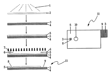
1 S FIG.1 shows a method of fabricating a working, counter, or reference
electrode
element in accordance with the present invention.
FIG. 2 shows another embodiment of a method of fabricating a working; counter,
or
reference electrode element in accordance with the present invention.
FIG. 3 shows a method of fabricating a reference or counter electrode element
in
accordance with the present invention.
FIG. 4 shows another embodiment of a method of fabricating a reference or
counter
electrode element in accordance with the present invention.
FIG. 5 shows an exploded view of the opposing electrode electrochemical sensor
in
accordance with the present invention. ~ ~ -
. FIG. 6 shows an assembled view of the opposing electrode electroblpemical
sensor of
FIG. 5. . - f;
FIGS. ?a ?h show a method of fabricating adjacent electrode elements for use
in an
adjacent electrode electrochemical sensor in accordance with the present
invention.
CA 02499867 1995-02-21
4
FIG. 8a shows a top view of FIG. 7g and FIG. 8b shows a top view of FIG. 'm.
FIG: 9 shows a dose response of one embodiment of a electrochemical sensor in
accordance with the present invention.
- 5..,;, . The adaptation of some PCB fabrication techniques to make
electrodes functional in
- ::biological fluids relies on electrochemical inertness in the potential
range of interest for
:; . , ensing, approximately -1 to +1 volts versus silver/silver chloride
(Ag/AgCI). In accordance
:. with the present invention, high quality thin noble metal films are used as
electrodes rather
than copper foil laminates. These thin metal films can be sputtered or
evaporatively
S ~Y
1.0 ~; ;:;deposited onto an appropriate foil material (e.g., polyester,
polycarbonate, polyimide) and
;:-then-laminated to a support substrate (e.g. by Courtaulds Performance
Fihns, Canoga Park,
California). Alternatively, the thin metal films may be deposited directly
onto the support
substrate. The resulting metallized substrate displays extremely small and
uniform grain size
(10-50 nm (nanometers) diameter), and importantly does not contain copper or
other
15.;,«;,electrocheriiically active materials. Such surfaces are nearly ideal
for the purpose of making
electrochemical measurements in biological or corrosive solutions. A second
insulating
,~ ;.;:;~. ubstrate is then applied to the metal layer and precisely patterned
to form an open electrt~oide
area and a meter contact pad. The combination of first insulating substrate,
metal, and
;,: ~-,.;aecond insulating substrate is referred to herein as an "electrode
element."
20 Two types of electrode elements are described below. The "opposing"
electrode
element is designed to be used in combination with a second opposing electrode
element,
separated by a spacer in a "sandwich" fashion. This embodiment is refenred to
as the
"opposing electrode electrochemical sensor." The opposing electrode
electrochemical sensor
includes a working electrode element and either a counter or a reference
electrode element as
25. ~ ~ described below. The "adjacent" electrode elements are fabricated on
the same substrate .
side-by side in a parallel fashion. This embodiment is referred to as the
"adjacent electrode
-:electrochemical sensor." The adjacent electrode electrochemical sensor may
include a
CA 02499867 1995-02-21
working electrode element and either a counter or a reference electrode
element, or may
include a working, counter and reference electrode element.
FABRICATION OF OPPOSING ELECTRODE ELEMENTS FOR TIC OPPOSING
5 ELECTRODE ELECTROCHEMICAL.SENSOR
A working, counter, or reference electrode element may be produced in
accordance
with the present invention as shown in FIG. 1. Electrically conducting
material 1 (e.g., a
noble metal or carbon) is vacuum sputtered or evaporatively deposited onto
thin support
material 2 (e.g., polyimide or other polymer such as polyester, polyethylene
terephthalate
10 (pET), or polycarbonate) to form electrically
conductive thin support material 3 (e. g_; by Courtaulds
Performance Films, Canoga Park, California). This step may or may not be
preceded by .
depositing, with the same means, a thin anchor layer of chromium, titanium, or
other suitable
material (not shown in FIG.I). The purpose of the thin anchor layer is to
increase adhesion
between electrically canducting material I and thin support material 2, as
well as to stabilize
I S the microstructure of electrically conducting material I .
Alternatively, electrically conducting material 1 can be deposited onto the
surface of
thin support material 2 by the method of electroless plating or a combination
of activation
and electroplating. These processes are well known but will be briefly
described. With
elcctroless plating, thin support material 2 is cleaned and if necessary
subjected to a surface
20 roughening step. The surface of thin support material 2 is then chemically
treated or
"activated" with a colloidal catalyst (e.g., PdCh-SnCl2 hydrosol) that adsorbs
strongly onto
the surface. The substrate and adsorbed catalyst should then be treated in an
"accelerator
bath", as is comraonly known in the electroless plating art, using an acidic
bath containing
PdCl2. Finally, thin support material 2 is plated in an electroless plating
bath designed to
25 deposit a thin layer of electrically conducting material 1 onto the surface
of thin support
material 2.
With electroplating, thin support material 2 is first activated using a
commercial
surface tresimeat (such as that available from Solution Technology Systems,
Inc.). Thin
CA 02499867 1995-02-21
6
support material 2 may then be electroplated in a manner well known to the
electroplating
industry with electrically conducting material 1, thereby forming metallized
thin support
substrate 3.
Metallized thin support material 3 is then laminated (e.g., by Litchfield
Precision
Components, Litchfield, Minnesota) to first insulating substrate 4 (e.g., a
bare fiberglass
. . ,,~, circuit.board such as 10 mil thick FR4 from Norplex/Oak, La Crosse,
Wisconsin, available as
product ED 130) using a suitable laminating adhesive system (e.g., Z-FLEXi'M
adhesive
...;system from Courtaulds Performance Films, Canoga Park, California). First
insulating
. r substrate 4 could be any suitable non-conductive glass or plastic
substrate with the desired
, supportive rigidity. In this step metallized thin support material 3 and
first insulating
. substrate 4 could optionally be laminated using a hot press.
. Once metallized thin support material 3 is supported on first insulating
substrate 4,
y metallized thin support material 3 can be processed with a suitable solder
resist to form an
. electrode area and a contact pad area for insertion into a meter and a power
source. The
surface of metallized thin support material 3 is cleaned with a suitable
solvent system (e.g., a
chloroflurocarbon solvent) and coated with second insulating substrate 5, a
commercial
' ~ - solder resist, either by screen printing or flood coating and then dried
according to the
manufacturer's specifications. An example of a commercial solder resist that
could be used is
_ s ,_ : ENPLATE~DSR 3242 solder resist from Enthone-OMI, Inc. (a negative
resist). The second
-.insulating substrate 5 is exposed to ultra-violet light rays 7 through
photomask b. As a result,
.~ a latent image is generated in second insulating substrate 5 rendering it
insoluble in a
r.;developer solution in those areas that were exposed to ultra-violet rays 7.
Before developing,
:. mask 6 is removed. The type of developer solution that should be used is
process-dependem
and generally will be specified by the manufacturer of the resist. Processing
in the developer
-: . solution removes portions of second insulating substrate 5, thus forming
first cutout portion 8
and second cutout portion 9. Following this procedure, the remaining second
insulating
-~.;.f ; substrate 5 maybe permanently cured by a suitable combination of heat
and ultra-violet light,
.,irmaking it a good barrier layer for applications in biological fluids. In
addition to the negative
CA 02499867 1995-02-21 =~
solder resist described above, positive resists may also be used in accordance
with the present
invention. In the case of a positive solder resist, the resist used is
insoluble in the developing
solution, unless the resist is exposed to electromagnetic radiation as
specifiedby the
manufacturer of the resist. _ . a:,::
As a result of the photol'rthographic process described above; first cutout
portion 8
and second cutout portion 9 are formed in second insulating substrate 5,
exposing the
underlying metallized thin support material 3. In finished electrode element I
lthe area of
first cutout portion 8 defines the electrode area and second cutout portion 9
acts as a contact
pad between electrode element 11 and a meter and a power source. When
electrode element
11 is a reference electrode element, a reference electrode,material (e.g.,
#DB2268
silver/silver chloride ink from Acheson Colloids Co., Port Huron, Michigan) is
a~di4onally
applied to the electrode area defined by first cutout portion 8.
Importantly, although it is common when using photolithography to remove the
resist
layer, in the present invention second insulating substrate 5 is not removed
and acts as an
insulating substrate in the finished electrochemical sensor. In addition, vent
port 10, which
extends through second insulating substrate 5, metallized thin support
material 3, and first
insulating substrate 4, may be included and used as a vent port for the
capillary space
(described below) in the finished electrochemical sensor and/or as a means of
introducing the
sample to the capillary space. At this stage, any reagent that is required may
be dispensed
onto the appropriate electrode areas as described below.
As an alternative to applying the second insulating substrate and performing
photolithography to define the working electrode area and contact pad as
described above, a
thin-film dielectric material may be screen printed onto metallized thin
support material 3.
The thin-film dielectric material may be W-curable (e.g., #ML-25198 from
Acheson
Colloids or #5018 from DuPont Electronics) or heat-curable (e.g., #7192IvI
From Metech).
The thin-film dielectric material can be applied through. a screen in a
specific pattern so as to
define first cutout portion 8 and second cutout portion 9 in the thin-film
dielectric material,
exposing the underlying metallized thin support, material 3. In the finished
electrode element,
CA 02499867 1995-02-21
a
8
the area of first cutout portion 8 defines the electrode area and second
cutout portion 9 acts as
a contact pad between the electrode element and a meter and a power source.
The thin-film
dielectric material can be chosen such that it may be cross-linked
photochemically aRer
application to the metallized thin support material, thus increasing stability
and adhesion to
- ~ the surface of the metallized thin support material as well as forming an
impenetrable barrier
-'layer for use in biological media. The thin-film dielectric material also
acts as an insulating
substrate in the finished electrochemical sensor. A vent port may also be
included and used
as a means of introducing the sample in the finished electrochemical sensor as
discussed
-'vbove. .
. . .. = Another method that may be used to fabricate a working, counter, or
reference . .
. .= : ~ electrode element in accordance with the present invention is shown
in FIG. 2. In this
embodiment, the electrically conducting material is deposited directly onto a
more flexible
.. ~ first insulating substrate, thus facilitating a less-expensive, semi-
continuous production
method: Electrically conducting material 12 is vacuum sputtered or
evaporatively deposited
; ~ directly onto first insulating substrate 13 (e.g., by Courtaulds
Performance Filins, Canoga
.. _ . . -...Park; California). An example of a suitable substrate is MYLARTM
substrate (from DuPont)
of approximately 10 mil thickness. Other suitable plastic, glass or fiberglass
substrates may
_, ,. . also be used. -Alternatively, electroless or electroplating techniques
as described above could
.. ,.. ; : be used to deposit metal 12 onto first insulating substrate 13.
Electrically conducting material 12 is then coated with second insulating
substrate
-; X14; such as a liquid negative solder resist (e.g., PROBOMER"''" solder
resist from Ciba-
v.Geigy) via a flood or dip coating while still in a roll form and then dried
using a suitable
combination of infrared and thermal heating. Second insulating substrate 14 is
exposed to
ultra-violet light rays 16 through photomask I 5. A latent image is generated
in second
: insulating substrate 14 as described above and following removal of mask 15
and processing
in the developer solution, portions of second insulating substrate 14 are
removed forming
first cutout portion 17 and second cutout portion I 8. (As an alternative to
the application of
~; ~ >second insulating substrate 14, it is also possible to screen print a
layer of dielectric ink in a
CA 02499867 1995-02-21
9
specific pattern equivalent to that obtained via the exposure process
disclosed above.)
Second insulating substrate 14 may also be permanently cured as
described~above. In
addition, solder resists other than described above (e.g., positive resists)
may be used in
accordance with the present invention.
5 In finished electrode element 20, the area of first cutout portion 17
defines the
electrode area and second cutout portion 18 acts as a contact pad between
electrode element
20 and a meter and a power source. As described above, when electrode element
20 is a
reference electrode element, a reference electrode material (e.g., #DB2268
silver/silver
chloride ink from Acheson Colloids Co., Port Huron, Michigan) is additionally
applied to the
10 electrode area defined by first cutout portion 17.
The method described above for producing electrode elements utilizing a
flexible
first insulating substrate allows for a continuous production process, in
which the metal is
deposited on a roll of the first insulating substrate. The metallized plastic
roll is then coated
with the second insulating substrate and processed through an in-line exposure
tool to expose
15 a series of the desired patterns (electrode areas and contact pads) in the
second insulating
substrate along the roll. This is followed by a developing cycle, according to
the
manufactwer's specifications and familiar to those skilled in the art,
followed bya curing
cycle. This results in similarly exposed areas of metal for the electrode
areas and the contact
pad areas, although the array of multiple electrodes is supported on a
continuous roll of
20 plastic. Reagent is then dispensed onto the electrode areas defined in the
second insulating
substrate. An adhesive spacer layer (described below) is then applied via
continuous roll
lamination. to the second insulating substrate (or dielectric ink). A second
roll of electrodes is
then fabricated as described above and laminated to the first roll so as to
form a capillary
chamber which exposes the active electrode areas as well as the reagent. The
multiple
25 sensors so defined on a continuous roll of material are then punched or die
cut from the web
prior to packaging.
As described above, a standard PCB substrate (a copper layer laminated to a
fiberglass substrate) is inappropriate for use as a working electrode in an
electrochemical
CA 02499867 1995-02-21
z
sensor.since it interferes with the electrochemical measurement. Specifically,
when a
;. mediator is being oxidized at the working electrode surface (anodic
process), copper may
:. also be, oxidized and therefore interfere with the electrochemical
measurement. However,
when reduction is occurring at the surface of a reference or counter electrode
(cathodic
5 process), a standard PCB substrate may be used in the reference or counter
electrode since
.. copper will not be reduced and therefore will not interfere. One embodiment
of a reference
_~ or counter electrode using a standard PCB as the first insulating substrate
will now be
described.
Referring to FIG. 3, a standard PCB substrate, which includes copper layer 30
10 laminated to fiberglass substrate 31, is used as a first insulating
substrate. .Electrically
f , _ conducting material 32 (e.g., #DB2268 silver/silver chloride ink from
Acheson Colloids, Port
Huron, Michigan) may be screen printed directly onto copper layer 30, leaving
cutout portion
33 exposed. Finally, spacer 34 (e.g., Ml'LAR'i'M substrate with double-sided
adhesive),
which includes first cutout portion 35 and second cutout portion 33, is placed
on top of
. 15 ~; electrically conducting material 32. Spacer 34 may also be any other
suitable plastic or
fiberglass. First cutout portion 35 and second cutout portion 33 may be cut
out by using a
laser process (e.g., by Laser Machining Ine., Somerset, Wisconsin). In
finished reference or
counter electrode element 37, the area of first cutout portion 35 exposes
underlying
electrically conducting material 32 and defines the reference or counter
electrode area.
: : : -Second cutout portion 33 exposes underlying copper layer 30 and acts as
a contact pad
between reference or counter electrode element 37 and a meter and a power
source. In
-! addition; vent port 36, which extends through spacer 34, electrically
conducting material 32,
:;~ :~;copp~r layer 30, and fiberglass substrate 31, may be included and used
as a vent port for the
:,-rcapillary space and/or as a means of introducing the sample to the
capillary space as
~ ,described above.
Another method that may be used to fabricate a reference or counter electrode
y .element in accordance with the present invention is shown in FIG. 4. A thin
anchor or
.; ::stabilizing layer of first electrically conducting material 38 (e.g.,
palladium) is sputtered or
CA 02499867 1995-02-21
11
evaporatively deposited onto thin support material 40, followed by a thicker
layer of second
electrically conducting material 39 (e.g., silver), to form metallized thin
support.r~iaterial 41
(e.g., by Courtaulds Performance Films, Canoga Park, California). As described
above, thin
support material 40 may be a polyimide or other polymer such as polyester,
PET; or
polycarbonate. Metallized thin support material 41 may then be Laminated to
first insulating
substrate 42, which may be fiberglass, glass, or plastic as described above.
.Alternatively,
first electrically conducting material 38 may be directly sputtered or
evaporatively deposited
onto first insulating substrate 42 rather than onto thin support material 40.
$pacerv43, which
includes fast cutout portion 44 and second cutout portion 45, is placed on top
ofinetallized
thin support material 41. Spacer 43 may be MYLAR'i'M substrate with double-
sided adhesive
as described above or any other suitable plastic or fiberglass. Finally, when
second
electrically conducting material 39 is silver, a solution of FeCl3 (not shown)
maybe
dispensed into first cutout portion 44 of spacer 43, where a layer of silver
chloride 46 is
formed by an oxidative process. The process of defining a reference electrode
area can also
optionally be assisted by applying and patterning a photoresist layer onto the
surface of ~ '
metallized thin support material 41 prior to treatment with FeCl3.
Alternatively; selected
regions of metaLlized thin support material 41 may be dipped into solutions of
FeCl3 to
achieve the same result. In finished reference or counter electrode element
48; the area of
first cutout portion 44 exposes layer 46 and defines the reference or counter
electrode area.
Second cutout portion 45 exposes metallized thin support material 41 and acts
as a-contact
pad between reference or counter electrode element 48 and a meter and a power
source. In
addition, vent port 47, which extends through spacer 43, metallized thin
support material 41,
and first insulating substrate 42, may be included and used as a means of
introducing the
sample in the finished electrochemical sensor as described above.
OPPOSING ELECTRODE ELECTROCI3EMICAL SENSOR
One embodiment of an electrochemical sensor with an opposing electrode design
in
accordance with the present invention is shown in FIGS. 5 and 6. Reference or
counter
CA 02499867 1995-02-21
1Z
electrode element 48 is spatially displaced from working electrode element 11
by spacer 43.
. -, (Spacer 43 is normally affixed to reference or counter electrode element
48 during
fabrication, but has been shown separate from element 48 for the purpose of
FIG. 5.) First
-,cutout portion 44 in spacer 43 forms capillary space 49 when situated
between reference or
-::. counter electrode element 48 and working electrode element 11. First
cutout pofion 8 in
working electrode element I 1 exposes metallized thin support material 3, the
working
_ : electrode area, which is exposed to the capillary space 49. First cutout
portion 44 in spacer
. , ~ 43, when afF~xed to reference or counter electrode element 48, defines
reference or courner
electrode area 46 (shown in phantom lines in FIG. 5), which is also exposed to
capillary
:10 ..., space 49.. ,Second cutout portions 9 and 45 expose metallized thin
support materials 3 and 41
respectively and act as contact pads between electrochemical sensor 52 and a
meter and a
power source.
. ,. ~ ;. . In assembled electrochemical sensor 52 shown in FIG. 6, capillary
space 49 (shown
. ,_:. . ,. ,phantom lines) has first opening 50 at one edge of the
electrochemical sensor. In addition,
; .., :vent port 10 in working electrode element andlor vent port 47 in
reference or counter
:;.,, ,:. electrode element 48 may be used to provide second opening 51 into
capillary space 49. The
,, vent<port may optionally be used as a means of introducing the sample to
the capillary space:
~.~" ,,t ,~, In use, a sample containing an analyte to be detected or measured
may be introduced into
<; -capillary space 49 of electrochemical sensor 52 through either opening 50
or vent port 51. In
:..;. either case, the sample is spontaneously drawn into the electrochemical
sensor by capillary
action. (Preferably, a surfactant is included in the capillary space to aid in
drawing the
. apple into the capillary space.) As a result, the electrochemical sensor
automatically
controls the sample volume measured without user intervention. In addition,
since the
sample is totally contained within capillary space 49, contamination of the
meter into which
electrochemical sensor 52 is inserted and the patient could be reduced or
eliminated, a
significant advantage when the sample is blood or a biological fluid.
CA 02499867 1995-02-21
13
FABRICATION OF ADJACENT ELECTRODE E.LEMENT'S FOR THE
ADJACENT ELECTRODE ELECTROCHEMICAL SENSOR
Adjacent electrode elements may also be produced in accordance with the
present
invention to form an adjacent electrode electrochemical sensor as indicated in
FIGS. 7 & 8.
The process is similar to that described above for the opposing electrode
elements. However,
since the electrodes are on the same support substrate next to each other, an
additional metal
etching step is involved. Electrically conducting material 61 (e.g., a noble
metal) is vacuum
sputtered or evaporatively deposited onto thin support material 62 (e.g.,
polyimide or other
polymer such as polyester, PET, or polyearbonate) to form metallized thin
support material
63 as described above. (FIGS. 7a-7b.) This step may or may not be preceded by
depositing a
thin anchor layer. Alternatively, electrically conducting material 61 can be
deposited onto
the surface of thin support material 62 by the method of electroless plating
or a combination
of activation and electroplating as described above. MetaIliud thin support
material 63 is
then laminated to first insulating substrate 64 (e.g., a bare fiberglass
circuit board such as 10
I S mil thick FR4) using a suitable laminating adhesive system (e.g., Z-
FLEXi'M adhesive system
from Courtaulds Performance Films, Canoga Park, California). (FIG. 7b.) First
insulating
substrate 64 could be any suitable non-conductive glass or plastic substrate
as described
above. - In this step metatlized thin support material 63 and first insulating
substrate 64 could
also be laminated using a hot press.
The surface of metalli~ed thin support material 63 is then cleaned with a
suitable
solvent system and then coated with photoactive etch resist 65. (FIG. 7c.)
Either positive or
negative etch resists may be used. The coating method will depend on whether a
semi-
aqueous or liquid resist is used. The semi-aqueous resists are generally
applied by a
lamination process, whereas the liquid resists are dip-coated, spray-coated,
curtain-coated, or
screen printed. Specifically, in the case of a negative, semi-aqueous resist
from DuPont, sold
under the trade-mark RESISTON, the resist is applied by
a hot roll lamination process. Photoactive etch resist
65, metallized thin support material 63, and first
insulating substrate 64 are then exposed to ultra-
violet light 67 through photomask 66 and baked
for 15 minutes
CA 02499867 1995-02-21 . .
i
14
-~- at 180°F. (FIG. 7d.) As a result, a latent image is generated in
photoactive etch resist 65
rendering it insoluble in a developer solution in those areas that were
exposed to ultra-violet
. rays 6~~ Processing in the developer solution removes the unexposed areas of
photoactive
etch resist 65, thus exposing portions of underlying metallized thin support
material 63.
, - (FIG. .7e.)
The entire substrate is then placed in a bath containing a chemical etchant
(e.g., when
electrically conducting material 61 is gold, an aqua regia or a solution of KI
and Iz may be
used) and incubated with constant stirring at a controlled temperature. The
etchant dissolves
~e exposed metallized thin support material 63, but is unable to dissolve the
portions of
metallized thin support material 63 that are covered with photoactive etch
resist 65. (FIG.
7f.) Photoactive etch resist 65 is then removed with a solvent revealing
metallized thin
support material 63 in the desired electrode pattern. (FIGS. 7g & 8a.) The
electrode pattern
- may include, for example, contact pads 69, leads 70, and electrode areas 71.
(FIG. 8a)
Finally, leads 70 are insulated with second insulating substrate 68, which may
be a solder
resist or a screen printable dielectric as described above for the opposing
electrode design.
(FIGS. 7h & 8b.)
In accordance with the present invention, the counter electrode may then
optionally
be converted to a reference electrode by electroplating silver directly onto
the counter
electrode; followed by treatment with FeCl3 to convert the silver surface to
silver chloride.
. ,. To facilitate this process a sacrificial interconnecting bus could be
designed into the layout to
allow multiple electrodes to be electroplated in one step. The other areas of
metal would
need to be protected during the plating step since it is generally done as a
batch process. This
could be accomplished with an etch resist in a manner similar to that
described above for the
adjacent working/counter electrode arrangement. Alternatively, a layer of
reference electrode
-material (e.g., silver chloride ink) may be screen printed on top of the
metal layer to yield a
reference electrode.
CA 02499867 1995-02-21 ,-~~,
4
IS
REAGENT
Many different types reagents may be applied to the working electrode and/or
the
reference or counter electrode to provide for a fully functional sensor whose
signal is
selective for and sensitive to the concentration of an analyte (e.g.,
glucose). These reagents
can be dispensed onto the working electrode area of the electrochemical
sensors described
above using an automated mechanical dispenser, screen printing, slot or roll
coating, spin
coating, blade coating, or ink jet printing. (Sometimes, both working and
counteTelectrode
areas will be coated with a reagent.) The reagents thus dispensed form a thin
coating over the
electrode which is rapidly swollen upon application of the sample (e.g.,
bloody at which time
a suitable potential may be applied to the electrodes and a current
measurement.made. ..The
current measurement may then be related to the concentration of the target
aualyte is the
sample. The use of polymeric materials and a capillary chamber to contain the
reagent
greatly reduces the risk of contamination by chemicals in the sensor of the
open wound in the
patient's finger. .
An example of a reagent tbat may be used with the present invention for the
detection
of glucose in a whole blood sample, designed to be used with the opposing
electrode
electrochemical sensor having a working electrode element and a reference
electrode
element, will now be described. The components of the reagent are listed
below: in table 1.
Table 1- reagent components
Com oaeat Amount
2-(N-morpholino) ethanesuiphonic100 millimolar
acid (mtvl)
S Buffer
Triton X-100 0.08% wt/wt
Polyvinyl alcohol (PVA),i.00% wt/wt
mol. weight IOK,
88% h dm zed
Imidazole osmium mediator6.2 mM
(reduced form -
nthesis described below
_
Glucose Oxidase 6000 units/ml
Following is a description of how the reduced form of the imidazole osmium
mediator was synthesized. The osmium intermediate (Os(bpy~Cl2) was fwst
synthesized,
followed by the reduced form of the imidazole osmium mediator
[Os(II)(bpy~(im~l]+[Cl]-.
CA 02499867 1995-02-21
( 4
16
("bpy" is a shorthand abbreviation for 2-2'-bipyridine and "im" is a shorthand
abbreviation
for imidazole.)
SYNTHESIS OF OSMIUM INTERMEDIATE
1) 19.335 g K20sC16 (0.04019 mole - from Aldrich) and 13.295 g bpy (0.08512
mole .
S . - from Aldrich) were weighed and transferred into a 1000 ml 1-neck flask.
2) 400 ml N,N'-dimethylformamide (DMF - from Mallinckrodt) was added to the
' flask to dissolve all reactants.
3) The flask contents were heated to reflex ( 1 S2-54°C) with stirring:
Reflex was
maintained for 1 hour with lower heat (setting was decreased from 100~/o to
6S% on variable
1!0 . ~ - transformer) to avoid overboiling.
4) The heat was turned off and the flask was cooled with continued stirring to
30-
40°C in 1-2 hours.
w . S) The mixture was filtered with vacuum using a medium grade glass fritted
filter
(1 SO ml).
:1 S >. - . 6) ~ The flask was rinsed with 20 ml DMF and poured into the
filter.
. . ~; ~ ~e filtered DMF solution was transfer ed to a 3 liter (1) beaker.
~;,...~-: : :===. 8) 22.?99 grams NaiS204 (from MaIlinckrodt) was weighed and
transferred to a
. °r~ separate 2 I beaker.
9) 21 deionized water was added to the beaker to dissolve the Na2S20d.
20 ' ~ 10) The Na2S204 aqueous solution was transferred to a dropping funnel
and added
dropwise (about S drops/second), over a period of 45 minutes, to the stinging
DMF solution.
11) The mixture was cooled in an ice bath for more than 3 hours.
12) The cooled mixture was filtered with vacuum using Whatman qualitative
filter
paper in a ceramic filter.
2S 13) The filtered product was washed twice with SO ml H20; twice with SO mI
methanol; and twice with SO ml diethyl ether.
14) The product, Os(bpy~Cl2, was dried under high vacuum (about 30 in. Hg) at
SO°C for more than 1 S hours (overnight).
CA 02499867 1995-02-21
. . ,
A n a
17
15) The product was weighed, transferred to a brown bottle having a screw-on
cap,
and stored in desiccator at room temperature. Yield: theoretical = 23.35 g,
actual =15.56 g,
yield = 66.6%.
SYNTHESIS OF THE REDUCED FORM OF THE IMIDAZOLE OSMIUM
S MEDIATOR
I) 14.01 g Os(bpy~Cl2 (0.0244 mole) and 2.30 g imidazoie (0.0338 mole - from
Aldrich) were weighed and transferred into a 2000 ml I-neck flask.
2) 600 ml ethanol and 600 ml deionized water were added to dissolve all
reactants.
3) The flask contents were heated to reflux with stirring and reflux was
maintained
for 6 hours with lower heat (setting was decreased from 90% to 60% on variable
transformer)
to avoid overboiling.
4) The heat was turned off and the flask cooled with continued stirring to 30-
40°C
over a period of 1 hour.
5) Half of the solution was transferred to a 1000 ml I-neck flask and the
solvents
were rotary evaporated. The remainder of the solution was added to the flask
and the
solvents were rotary evaporated.
6) The dried product was rinsed on the flask wall with 50 ml ether and the
ether
wash was discarded.
7) The product was dried under high vacuum (about 30 in. Hg) at 50°C
for more than
15 hours (overnight).
8) The flask wall was scraped to collect the product,
[Os(II)(bpy}~(im)Cl]+[CI]-.
The product was weighed and transferred to a brown bottle having a screw-on
cap. The
bottle was stored in a desiccator at room temperature. Yield: theoretical
=16.3 g, actual =
- 16.1 g, yield =-98.8%. -
Following is a description of how the reagent described in table=1
fiv~s~prepared and
used in combination with opposing electrode elements to form an
electrochemical sensor.
1) Polymer matrix
CA 02499867 1995-02-21 - .
18
,; ; ; :;.; ;-. ~_ :; : . --, a) 1.952 g MES buffer was added to 85 ml
nanograde water. The mixture
~. s .. t :.... - was stinTed until dissolved. The pH of the solution was
adjusted to 5.5
with NaOH and the total volume of the solution was brought to 100 ml.
,: ; , . b) 0.08 g of Triton X-100 and 1 g of PVA was added to a 150 ml
beaker.
$ Buffer solution was added to bring the total weight of the solution to 100
g. The mixture was then heated to boiling to dissolve the PVA.
2) Coating mixture
;,: . ~ a) 4.0 mg of the reduced osmium mediator, [Os(II)(bpyh(im)Cl]'~[Cl]',
was
added to 1 ml of the polymer matrix. The mixture was vortexed to
r 1.0 ; ... .- dissolve the mediator. 6000 units of glucose oxidase was added
to the
mixture and the solution was mixed until the enzyme was dissolved.
. ~ ; -: , Although the reagent described above is preferred for use with this
invention, other
types of reagents,, which are specifically reactive with an analyte in a fluid
sample to produce
. ,. an electrochemically-measurable signal which can be correlated to the
concentration of the
15 ,:analyte in the fluid sample, may be used. The reagent should include at
least a mediator and
an enzyme. Preferably, the reagent should also includes a buffer, a film
former, and a
t t :.., surfactant as described above.
Other redox mediator systems could also be utilized (e.g., using potassium
I , . .:. ferricyanide as the redox mediator rather than the imidazole osmium
mediator described
20 above) as well as redox polymer systems (in which the mediator and enzyme
are immobilized
s --- : on the electrode surface).
..a.: ,7F:Ls.. ...
.,.,. .. .., : ._. . USE OF THE ELECTROCHEMICAL SENSOR
The electrochemical sensor described above may be used for, but is not limited
to, .
25. ,-; ;:~the~determination of blood glucose levels using a small drop of
blood (3-20p1) obtained from
.. . . ,.
. ">ts~,;the patient's finger or other location by the use of a lancing
device. A significant advantage
to the present invention is the low volume required for the measurement, thus
allowing for a
very low pain lancet device which produces low sample volumes.
CA 02499867 1995-02-21
19
An example of how an opposing electrode electrochemical sensor was made and
used
to determine the concentration of glucose in a whole blood sample will now be
described. A
reference electrode element was fabricated as described above, having gold as
the~electrically
conducting material and having a spacer attached to expose a portion of the
gold (capillary
space). A silverlsilver chloride polymer thick film ink (Acheson Colloids DB
2286) was
thinned 2:1 wt/wt with butoxyethanol. 2.5 pl of the resulting mixture was
applied to the
capillary space and spread to fill the capillary area. The electrode was then
dried for 15
minutes at 90°C. . . .
A working electrode element was fabricated as described above; having:gold as
the
electrically conducting material. 1 pl of the coating mixture (from the
reagent example
described above) was then applied to the working electrode surface of the
working electrode
element. The coated electrode was dried at 45°C for 15 minutes.
The working electrode element was then "sandwiched" together with the
reference
electrode element as described above and as illustrated in FIGS. 5 & 6 to form
the completed
electrochemical sensor. The completed electrochemical sensor was used, as
described below,
to perform a glucose assay. The working electrode potential was made +200
millivolts (mv)
versus the Ag/AgCI reference electrode by a potentiostat. 10 ltl of spiked
glycolyzed venous
blood was added to capillary space 49 through first opening 50. Current was
measured 10
seconds after applying the sample to the electrochemical sensor. FIG. 9 shows
a dose
response curve generated by the assay of spiked glycolyzed venous blood
samples with
different levels of glucose.
It is intended that an electrochemical sensor made in accordance with the
present
invention should be inserted into a small meter device where the contact tabs
can make
electrical contact with the measuring circuit within the meter. The meter will
normally be
adapted to apply an algorithm to the current measurement, whereby the ana~yte
level is
provided and visually displayed. Examples of improvements in such a power
source and
meter are the subject of commonly assigned U.$. Patent Number 4,963,814 -
"Regulated
Bifurcated Power Supply" l,Parks et al., issued October 16, 1990), U.S. Patent
Number
CA 02499867 1995-02-21
4,999,632 - "Analog to Digital Conversion with Noise Reduction" issued Match
12,
1991 U.S. Patent Number 4,999,582 - "Electrochemical sensor Electrode
Excitation Circuit"
(p~g~" issued March 12, 1991), and U.S. Patent No. 5,243,516 - "Biosensing
Instrument and Method" Q~hitg, issued September 7, 1993).
5
The present invention has been disclosed in the above teachings and drawings
with
sufEcient clarity and conciseness to enable one skilled in the art to make and
use the
invention, to know the best mode for carrying out the invention, and to
distinguish it from
other inventions and from what is old. Many variations and obvious adaptations
of the
10 invention will readily come to mind, and these are intended to be contained
within the scope
of the invention as claimed below.