Note: Descriptions are shown in the official language in which they were submitted.
CA 02499944 2005-03-22
WO 2004/032190 PCT/US2003/030636
INTEGRATED DISPLAYS USING NANOWIRE TRANSISTORS
BACKGROUND OF THE INVENTION
Field of the Invention
[0001] The present invention relates to displays, and more particularly,
integrated displays using nanowire transistors.
[0002] A wide variety of display technologies exist. These display
technologies include liquid crystal displays, organic light emitting diodes
(OLED) displays, nanotube field effect displays, plasma displays, micromirror
displays, micoelectromechanical (MEMs) displays, electrochromic displays
and electrophoretic displays. Each of these display types has unique
characteristics that make a display type more or less suitable for a
particular
display function (e.g. a computer display, a watch display). Nonetheless, each
display type: shares common features associated with a backplane that can
include pixels, electronics to drive' changes in the appearances of the pixels
and a base substrate, such as glass. A detailed description of a liquid
crystal
display - one of the more common types of displays - is provided to highlight
the characteristics of displays.
[0003] A liquid crystal display (LCD) is a display made of material whose
reflectance or transmittance of light changes when an electric field is
applied.
Liquid crystal displays are used in a plethora of applications ranging from
wristwatch displays to laptop computer displays to television screens. As the
name suggests, fundamental components of an LCD are liquid crystals.
Liquid crystals have several unique properties that make LCAs possible. One
liquid crystal feature is that they are affected by electric fields. The most
common form of liquid crystal used in LCDs is called a twisted nematic liquid
crystal. As is well known by persons skilled in the relevant arts, these
crystals
respond predictably to the application of an electric field to control the
amount
of light passage through the crystal. Liquid crystals are arranged to form
pixels within the display. A pixel is the smallest discrete element of an
image
CA 02499944 2005-03-22
WO 2004/032190 PCT/US2003/030636
-2-
on the LCD. Typically, the greater the number of pixels per unit area (e.g.,
square-inch) the greater the resolution.
[0004] Another critical element of LCDs, as well as the other display
technologies, is the electronics used to control and drive the liquid crystals
or
the particular component used in a display technology (e.g., micromirrors,
plasma, a nanotube, etc.). The complexity of the electronics varies greatly by
the application and LCD type. For example, two common types of LCDs are
passive and active matrix LCDs. Within a passive matrix LCD, a simple
conductive grid is used to supply current to the liquid crystals that form the
pixels. The grid is formed by columns and rows of transparent conductive
material, typically indium-tin oxide. To turn on a pixel, a voltage is applied
to
a column and its negative is applied to a row that intersects at the
designated
pixel to deliver a field that untwists the liquid crystals at the pixel to
allow
light to be transmitted or reflected. The electronics to drive a passive
matrix
LCD are relatively simple. The tradeoff for the relatively simple electronics
is
that each pixel of a passive matrix LCDs has a duty cycle that gets smaller as
the number of pixels increases. This results in slow response times and poor
contrast. As a result, an LCD's ability to refresh an image can be slow and
the
images not crisp.
[0005] An active matrix LCD has more complex electronics to cause each
pixel to have its electric field applied nearly one hundred percent of the
time.
This enables very short response times for exercising the liquid crystals,
high
contrast, and direct pixel addressing to make active matrix LCDs well suited
for video and fast graphic application. An active matrix LCD depends on thin
film transistors (TFT). Specifically, an independent TFT is associated with
each and every pixel. Likewise, with other technologies the more complex
they are, the more likely that they rely on TFTs.
[0006] FIG. 1 illustrates a typical active matrix LCD using TFTs, active
matrix LCD 100. Active matrix LCD 100 includes polarizer film 110, upper
glass substrate 120, color filter 130, transparent electrodes 140, liquid
crystals
150, pixel transistors and traces 160, edge electronics 170, base glass
substrate
CA 02499944 2005-03-22
WO 2004/032190 PCT/US2003/030636
-3-
180 and polarizer film 190. Collectively, the pixel transistors (and traces)
160, edge electronics (and traces) 170, and base glass substrate 180 can be
referred to as a backplane, or in this case an active matrix backplane (i.e.,
the
transparent (front) electrodes and the liquid crystal are not part of the
backplane). The term active matrix backplane can also be used to refer to the
above elements not including edge electronics 170. Each of these layers are
sandwiched together to create an LCD display that can be used, for example,
in a laptop computer display. In this case a frame would be added to support
the LCD and affix the display to the laptop base. Circuitry would exist to
enable communications from the laptop computer to the LCD to display the
desired graphics or video.
[0007] When an image is to be displayed by active matrix display 100,
electronic signals are sent using the TFTs and edge electronics to configure
the
liquid crystals located at the appropriate pixels such that no light or a
certain
fraction of the light is transmitted through the pixel. Edge electronics can
include shift registers, level shifters that match an outside signal to a
signal on
a display and output buffers. FIG. 2 illustrates the layout of the TFT and
edge
electronics. FIG. 2 includes a set of thin film column transistors 210A
through
210n, a set of thin film row transistors 220A through 220n, a set of
conductive
column traces 240A through 240n, a set of conductive row traces 250A
through 250n, a set of thin film pixel transistors, such as thin film pixel
transistor 230, and a set of pixels, such as pixel 260. A thin film pixel
transistor, such as thin film pixel transistor 230 will be associated with the
intersection of each row and column trace. A pixel is associated with each
intersection of a row and column trace. Pixel 260 provides one example of a
pixel. Thus, for example, when pixel 230 is to be addressed the appropriate
signals are transmitted to thin film column transistor 210A, thin film row
transistor 220A and thin film pixel transistor 260.
[0008] Currently, it is possible to use amorphous silicon thin film
transistors
(a-Si TFTs) or polycrsytalline silicon TFT (p-Si or poly-Si TFTs) or bulk-
silicon transistors as the row, column, and pixel transistors in LCD displays,
CA 02499944 2005-03-22
WO 2004/032190 PCT/US2003/030636
-4-
and a wide range of other types of displays. Use of these types of transistors
imposes several design limitations on displays. First, the performance
associated with transistors produced from a-Si or poly-Si is significantly
less
than those that use bulk silicon. The use of bulk silicon is often not
feasible
for pixel transistors, because the size of many commercially viable LCDs or
other display types is greater than the size of the silicon wafers used to
produce traditional bulk silicon transistors, and the cost of bulk silicon is
too
high for use as a pixel backplane. Additionally, because the LCD substrates
must be clear, silicon wafers used to fabricate bulk silicon transistors can
only
be used as the substrate for reflective displays. Second, a-Si and poly-Si
transistors are do not have adequate performance for the row and column
transistors, so that existing LCDs or other display types have a large number
of interconnects around the edge of a panel to hook up row and column traces
to external circuitry using crystalline silicon (i.e., bulk silicon)
transistors in
integrated circuits. These interconnects increase circuit and assembly
complexity and interconnect failure, and decrease manufacturing yield. Third,
the relatively large size of the a-Si and poly-Si circuitry and interconnects
add
weight to a display. Fourth, because of the relatively high temperatures
needed to produce a-Si and poly-Si devices, the choice of transparent
substrate
is largely limited to the use of glass, high-temperature glass or quartz.
[0009] What is needed is circuitry that has improved performance
characteristics that are comparable to those of circuitry using bulk silicon-
based devices, but that can be applied over areas larger than a typical
silicon
wafer at a low cost and at a temperature compatible with a large number of
transparent substrates.
[00010] What is also needed is circuitry that can be integrated within a LCD
panel and other displays to reduce system complexity and weight.
[00011] What is also needed is circuitry that can be applied to flexible
substrates, such as plastic.
CA 02499944 2005-03-22
WO 2004/032190 PCT/US2003/030636
-5-
SUMMARY OF THE INVENTION
[00012] The present invention is directed to displays using nanowire
transistors. In particular, a liquid crystal display using nanowire pixel
transistors, nanowire row transistors, nanowire column transistors and
nanowire edge electronics is described. A nanowire pixel transistor is used to
control the voltage applied across a pixel containing liquid crystals. A pair
of
nanowire row transistors is used to turn pixel transistors that are located
along
a row trace connected to the pair of nanowire row transistors on and off.
Nanowire column transistors are used to supply a voltage to nanowire pixel
transistors that are located along a column trace connected to a nanowire
column transistor. Nanowire edge electronics are used to control row and
column transistors. In alternative embodiments, a liquid crystal display using
combinations of nanowire transistors and other forms of transistors for the
pixel, row, and column transistors and edge electronics is presented. For
example, a liquid crystal display is provided that uses amorphous silicon
pixel
transistors with nanowire transistors for row and column transistors. In an
alternative embodiment of the invention, display technologies including
organic light emitting diodes (OLED) displays, nanotube field effect displays,
plasma displays, micromirror displays, micoelectromechanical (MEMs)
displays, electrochromic displays and electrophoretic displays using nanowire
transistors are also provided.
[00013] There are numerous benefits associated with the use of nanowire
transistors within a display. First, nanowire transistors can be positioned on
a
multitude of substrates including glasses and plastics. As a result, displays
can
be developed on flexible substrates that open up a plethora of applications
using flexible and/or rollable displays. Second, nanowire transistors have
superior performance when compared to a-Si and poly-Si TFTs, thereby
allowing the edge electronics associated with the row and column transistors
to be integrated between the row and column traces. This allows displays, in
particular LCDs, to be produced with an increased ratio of screen size to
frame
CA 02499944 2005-03-22
WO 2004/032190 PCT/US2003/030636
-6-
size for holding the screen and reduces the complexity of external control
circuitry. Furthermore, because nanowire transistors are small they reduce
obscuration associated with conventional a-Si and poly Si TFTs that is
typically quite poor, since the larger a-Si and poly Si TFTs tend to block a
significant portion of the light being reflected or transmitted through a
display,
such as an LCD. For emissive displays like OLEDs, smaller transistors allow
a larger portion of the backplane area to be occupied by the OLEDs
constructed directly on the backplane, rather than the more difficult process
of
building the OLEDs on top of the pixel transistor
(00014] Further embodiments, features, and advantages of the invention, as
well as the structure and operation of the various embodiments of the
invention are described in detail below with reference to accompanying
drawings.
BRIEF DESCRIPTION OF THE FIGURES
[00015] The invention is described with reference to the accompanying
drawings. In the drawings, like reference numbers indicate identical or
functionally similar elements. The drawing in which an element first appears
is indicated by the left-most digit in the corresponding reference number.
[00016] FIG. 1 is a diagram of an active matrix LCD.
[00017] FIG. 2 is a diagram of TFT and edge electronics used to address pixels
within an LCD.
(00018] FIG. 3A is a diagram of a LCD using nanowire transistors, according
to an embodiment of the invention.
[00019] FIG. 3B is a diagram of a detailed portion of an LCD using nanowire
transistors, according to an embodiment of the invention.
[00020] FIG. 4 is a diagram of four nanowire pixel transistors within an LCD,
according to an embodiment of the invention.
[00021] FIG. 5 is a diagram of a pair of nanowire row transistors within an
LCD, according to an embodiment of the invention.
CA 02499944 2005-03-22
WO 2004/032190 PCT/US2003/030636
_7_
[00022] FIG. 6 is a diagram of two-nanowire column transistors within an
LCD, according to an embodiment of the invention.
DETAILED DESCRIPTION OF THE INVENTION
[00023] It should be appreciated that the particular implementations described
herein are examples of the invention and are not intended to otherwise limit
the scope of the present invention in any way. Indeed, for the sake of
brevity,
conventional electronics, manufacturing, semiconductor devices, and
nanotube, nanorod, nanowire and nanoribbon technologies and other
functional aspects of the systems (and components of the individual operating
components of the systems) may not be described in detail herein. Moreover,
while the number of nanowires and spacing of those nanowires are provided
for the specific implementations discussed, the implementations are not
intended to be limiting and a wide range of the number of nanowires and
spacing can also be used. Furthermore, dimensions and compositions of the
nanowires can be varied. The implementations described are not intended to
be limiting and a wide range of dimensions and compositions can be used.
[00024] As used herein, the term "nanowire" generally refers to any elongated
conductive or semiconductive material that includes at least one cross
sectional dimension that is less than SOOnm, and preferably, less than 100 nm,
and has an aspect ratio (length:width) of greater than 10, preferably, greater
than S0, and more preferably, greater than 100. Examples of such nanowires
include semiconductor nanowires as described in Published International
Patent Application Nos. WO 02/17362, WO 02/48701, and 01/03208, carbon
nanotubes, and other elongated conductive or semiconductive structures of
like dimensions.
[00025] While the LCD model described herein principally is based on
properties associated with Si. Other types of nanowires can be used including
semiconductive nanowires that are comprised of semiconductor material
selected from, e.g., Si, Ge, Sn, Se, Te, B, C (including diamond), P, B-C, B-
CA 02499944 2005-03-22
WO 2004/032190 PCT/US2003/030636
-g_
P(BP6), B-Si, Si-C, Si-Ge, Si-Sn and Ge-Sn, SiC, BNBPBAs,
A1N/A1P/AIAs/AISb, GaN/GaP/GaAs/GaSb, InN/InP/InAs/InSb, BNBPBAs,
A1N/A1P/AIAs/AISb, GaN/GaP/GaAs/GaSb, InN/InP/InAs/InSb,
Zn0/ZnS/ZnSe/ZnTe, CdS/CdSe/CdTe, HgSBgSe/HgTe,
BeSBeSe/BeTe/MgS/MgSe, GeS, GeSe, GeTe, SnS, SnSe, SnTe, PbO, PbS,
PbSe, PbTe, CuF, CuCI, CuBr, CuI, AgF, AgCI, Agar, AgI, BeSiN2, CaCN2,
ZnGeP2, CdSnAs2, ZnSnSb2, CuGeP3, CuSi2P3, (Cu, Ag)(Al, Ga, In, Tl, Fe)(S,
Se, Te) Z, Si3N4, Ge3N4, A1203, (Al, Ga, In) z (S, Se, Te) 3, AlzCO, and an
appropriate combination of two or more such semiconductors.
[00026] In certain aspects, the semiconductor may comprise a dopant from a
group comprising: a p-type dopant from Group III of the periodic table; an n-
type dopant from Group V of the periodic table; a p-type dopant selected from
a group comprising: B, Al and In; an n-type dopant selected from a group
comprising: P, As and Sb; a p-type dopant from Group II of the periodic table;
a p-type dopant selected from a group comprising: Mg, Zn, Cd and Hg; a p-
type dopant from Group IV of the periodic table; a p-type dopant selected
from a group comprising: C and Si.; or an n-type is selected from a group
comprising: Si, Ge, Sn, S, Se and Te. Other known semiconductor dopants
can be used, as would be apparent to persons having ordinary skill in the art.
[00027] Additionally, the nanowires can include carbon nanotubes, or
conductive or semiconductive organic polymer materials, (e.g., pentacene, and
transition metal oxides).
[00028] Hence, although the term "nanowire" is referred to throughout the
description herein for illustrative purposes, it is intended that the
description
herein also encompass the use of nanotubes. Nanotubes can be formed in
combinations/thin films of nanotubes as is described herein for nanowires,
alone or in combination with nanowires, to provide the properties and
advantages described herein. In addition, nanotubes need not comprise purely
carbon, but can contain other materials such as boron or the like, as will be
recognized by one of skill in the art.
CA 02499944 2005-03-22
WO 2004/032190 PCT/US2003/030636
-9-
[00029] Furthermore, it is noted that a thin film of nanowires of the present
invention can be a "heterogeneous" film, which incorporates semiconductor
nanowires and/or nanotubes, and/or different compositions of nanowires,
and/or any combination thereof of different composition and/or structural
characteristics. For example, a "heterogeneous film" can includes
nanowires/nanotubes with varying diameters and lengths, and nanotubes
and/or nanotubes that are "heterostructures" having varying characteristics.
[00030] By substantially "aligned" or "oriented" is meant that the
longitudinal
axes of a majority of nanowires in a collection or population of nanowires is
oriented within 30 degrees of a single direction. Although the majority can be
considered to be a number of nanowires greater than 50%, in various
embodiments, 60%, 75%, 80%, 90%, or other percentage of nanowires can be
considered to be a majority that are so oriented. In certain preferred
aspects,
the majority of nanowires are oriented within 10 degrees of the desired
direction. In additional embodiments, the majority of nanowires can be
oriented within other numbers or ranges of degrees of the desired direction,
including randomly or isotropically oriented.
[00031] It should be understood that the spatial descriptions (e.g., "above",
"below", "up", "down", "top", "bottom", etc.) made herein are for purposes of
illustration only, and that devices of the present invention can be spatially
arranged in any orientation or manner.
[00032] Finally, while the discussion focuses on an exampled display type of
an LCD, the invention applies to any type of display technology that has a
backplane with electronics to drive changes in pixels, including, but not
limited to organic light emitting diodes (OLED) displays, nanocrystal-doped
OLEDs, nanotube field effect displays, plasma displays, micromirror displays,
micoelectromechanical (MEMs) displays, electrophoretic displays and the
like.
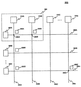
[00033] FIG. 3A provides LCD 300 using nanowire transistors, according to an
embodiment of the invention. LCD 300 includes a set of nanowire column
transistors 310A through 310n, a set of nanowire row transistor pairs 320A
CA 02499944 2005-03-22
WO 2004/032190 PCT/US2003/030636
-10-
through 320n, a set of nanowire pixel transistors 330A through 330z, a set of
conductive column traces 340A through 340n, a set of row traces 350A
through 350n, and a set of pixels 360A through 360z. Each nanowire column
transistor is coupled to a set of nanowire pixel transistors along a column
trace
extending from the nanowire column transistor. For example, nanowire
column transistor 310A is coupled to nanowire pixel transistors 330A, 330M,
and 3305 along column trace 340A. Each nanowire row transistor pair is
coupled to a set of nanowire pixel transistors along a row trace extending
from
the nanowire row transistor. For example, nanowire row transistor pair 320A
is coupled to a set of nanowire pixel transistors along row trace 350A. A
nanowire pixel transistor is associated with a corresponding pixel. For
example, nanowire pixel transistor 330A is associated with pixel 360A.
[00034] In addition, nanowire edge electronics (not shown in FIG. 3A) can be
used to control the nanowire column, row and pixel transistors. Nanowire
edge electronics can also be used to drive column, row and pixel transistors
that are now made using nanowires. Nanowire edge electronics can include
nanowire shift registers, nanowire level shifters and nanowire buffers.
Nanowire shift register refers to a shift register implemented using nanowire
transistors. Nanowire level shifter refers to level shifters implemented using
nanowire transistors. Nanowire buffer refers to a buffer implemented using
nanowire shifters. Other types of edge electronics can be implemented using
nanowire transistors.
[00035] In operation, when the intensity of a pixel is to be changed, a
voltage is
applied to a nanowire column transistor for the column in which the pixel is
located. The nanowire row transistor for the row in which the pixel is located
will be turned on to allow current to flow to the nanowire pixel transistor.
When the nanowire pixel transistor is on, current flows through the nanowire
pixel transistor to make the voltage across the pixel, approximately the same
as the voltage applied on the column to generate the desired intensity of
light
being transmitted through the pixel.
CA 02499944 2005-03-22
WO 2004/032190 PCT/US2003/030636
-11-
[00036] While FIG,3A demonstrates an embodiment in which column, row and
pixel transistors are nanowire transistors. In alternate embodiments any
combination of nanowire transistors and a-Si or poly-Si transistors can be
used
for the column, row and pixel transistors. For example, in one embodiment
the pixel transistors can be a-Si TFTs or poly-Si TFTs and the row and column
transistors can be nanowire transistors. This may be an appealing alternative
because the performance requirements for the pixel transistors are relatively
low, and can be easily met by a-Si TFTs. In another example, the column
transistors can be a-Si or poly-Si TFTs and the row and pixel transistors can
be
nanowire transistors. In another example, the row transistors can be a-Si or
poly-Si TFTs, and the column and pixel transistors can be nanowire
transistors. In another example, the pixel transistors and row transistors can
be
a-Si or poly-Si TFTs, and the column transistors can be nanowire transistors.
In another example the pixel transistors and column transistors can be a-Si or
poly-Si TFTs, and the row transistors can be nanowire transistors.
[00037] FIG. 3B provides a more detailed view of a portion 390 of LCD 300,
according to an embodiment of the invention. FIG. 3B highlights a number of
aspects of an LCD using nanowire transistors, namely that a pair of nanowire
row transistors will be coupled to each row trace and that each pixel has
resistance and capacitance associated with it that impact the design
considerations for the transistors. It should be noted that the row and column
traces will also have resistance and capacitance associated with them that
impact the design criteria. Nanowire row transistors 322 and 324 form
nanowire row transistor pair 320A, and are coupled to nanowire pixel
transistors 330A and 330B over row trace 350A. As described with respect to
FIG. 5 below in more detail, nanowire row transistors 322 and 324 are used to
turn nanowire pixel transistors, such as nanowire pixel transistor 330A and
330B on and off.
[00038] Additionally, FIG. 3B illustrates that each pixel will have a
capacitance
and resistance associated with the pixel. For example, pixel 360A includes
capacitance C~~a, capacitance CS and resistance R~~a. Capacitance Ci~a
CA 02499944 2005-03-22
WO 2004/032190 PCT/US2003/030636
-12-
represents the capacitance associated with liquid crystals within pixel 360A.
Resistance R~~a represents the resistance associated with liquid crystals
within
pixel 360A. Capacitance CS is a storage capacitance that is added to improve
performance.
[00039] Based on the teachings herein, a person skilled in the relevant arts
will
be enabled to incorporate nanowire transistors into an LCD without undue
experimentation. Furthermore, while the design tool demonstrates the use of a
particular type of nanowire transistor, the example is not intended to be
limiting. Rather individuals skilled in the relevant arts will be able to
apply
the teachings herein and the concepts used within the design tool discussed
below to develop integrated LCDs or other display types with a wide range of
nanowire semiconductors with varying characteristics, such as type of
nanocrystal materials, doping, number of wires and orientation.
[00040] The inventors developed a nanowire LCD design tool to demonstrate
the feasibility of using nanowire transistors for the electronics driving the
liquid crystals within pixels of an LCD. The tool includes a user interface,
an
LCD design input element, a nanowire characteristics input element, a
transistor requirements engine, and a nanowire design engine. The user
interface enables a user to enter design criteria and displays results. The
LCD
design input element gathers information about the type of LCD (e.g. LCD
size, pixel density, etc.). The nanowire characteristics input element gathers
information about nanowire characteristics, including size, nanowire crystal
material, doping, and related performance characteristics. The transistor
requirements engine generates the performance requirements needed for the
row, column and pixel transistors. The nanowire design engine receives as an
input the output of the transistor requirements engine and determines the type
of nanowire transistor needed for the particular application.
[00041] The nanowire LCD design tool was used to demonstrate that nanowire
transistors can be used to drive pixels within an LCD. The use of the tool
also
facilitated the identification of unique benefits associated with the use of
nanowire transistors within an LCD.
CA 02499944 2005-03-22
WO 2004/032190 PCT/US2003/030636
-13-
(00042] In the analysis, conservative assumptions were used for the nanowire
characteristics. In particular, a surface mobility (NS) of about one half the
typical values of bulk silicon was used with a standard fit for (~S) versus
doping to account for a reduction in mobility associated with doping. The
doping assumptions were that Na = 10~~/cm3 in the channel where the gate
controls the conductance of the transistor and Nd = 10~9/cm3 in the source and
drain where there is no gate control. The length of the channel, source and
drain were each assumed to be 10 Vim. These assumptions were conservative
to ensure that the lowest cost lithography could be used.
[00043] Additionally, a circumferential gate was assumed to be used, which
means that the gate contact surrounds the nanowire. Furthermore, it was
assumed that the nanowires would have a core shell design, with silicon oxide
grown around a nanowire core and a gate applied around the oxide. Using this
approach, a 60 nm diameter silicon core nanowire was assumed with a 40 nm
think SiOz shell, such that the nanowire had a 140nm total diameter. Finally,
conservative threshold and driving voltage were assumed, such that the
threshold voltage (Vt) was assumed to be two volts and the driving voltage
(Vd) was assumed to be five volts. Driving voltages for a-Si and poly-Si
transistors are typically higher. The voltages assumptions used are more in
line with voltages used within typical integrated circuits. U.S. Provisional
Appl. Nos. 60/414,323, filed Sept. 30, 2002 and 60/468,276, filed May 7,
2003, which are incorporated by reference herein in their entirety, describe
nanowire semiconductors and provide performance data that support these
assumptions. Note that similar backplane electronics can be fabricated
without the need for a conformal gate and/or conformal gate-oxide.
[00044] The LCD panel assumptions are based on typical characteristics of
existing LCD panels. In particular, the LCD panel was assumed to have a 21
inch diagonal display with a resolution of 1024 x 768 RGB pixels with a 60
Hz refresh rate. For each RGB pixel, three pixels (red, green and blue) exist.
Therefore, the column pitch would be approximately 110 Nm and the row
pitch would be approximately 330 Vim. A capacitance of one pF was assumed
CA 02499944 2005-03-22
WO 2004/032190 PCT/US2003/030636
-14-
to be associated with each pixel. The row traces were assumed to be aluminum
(Al) that was 10 Nm wide and 1 ~m thick. The row insulation was assumed to
be made from SiOz that was greater than 0.5 Nm thick. The column traces
were assumed also to be A1 that was 10 ~m wide and 2 ~m thick. The column
insulation was assumed to be made from Si02 that was greater than 2 Nm
thick. The choice of parameters for the row and column traces determines the
resistance and capacitance of the traces. In turn, the trace resistance and
capacitance, along with the pixel and transistor capacitances and resistances,
determines how fast the line can be switched, and what level of performance is
needed within the row, column and pixel transistors.
[00045) Based on these LCD criteria, the tool produced outputs that defined
the
requirements for the column, row and pixel transistors. Methods to size TFT
transistors will be known by individuals skilled in the relevant arts. See,
e.g.,
Satoru Tomita et al., Transistor Sizing for AMLCD Integrated TFT Drive
Circuits, Journal of the Society of Information Display 5/4, 1997 at 339-404.
Specifically, for the pixel transistors the model determined that an on
resistance less than 1.6 MOhms would be needed, and an off resistance greater
than 835 GOhms would be needed for the pixel transistors. Determination of
the on and off resistance are based on a variety of factors. In particular,
the off
resistance needs to be high to avoid the undesirable effect of flicker within
the
pixels. To avoid flicker, the capacitance voltage across the pixel has to
coast
for the 16.6ms between refreshes (assuming a 60Hz refresh rate) without
significant leakage. The leakage rate is a function of the off resistance of
the
nanowire pixel transistor. Leakage in the LCD resistance or the transistor
will
cause the voltage on the pixel to change during refreshes, which can induce an
undesirable flicker in the pixel. For the purposes of the analysis, it was
assumed that the voltage on the pixel should not change by more than 10%
between refreshes. On the other hand, the on-resistance needs to be low
enough to allow the pixel to charge in the time available. Factoring in these
criteria led to the on- and off resistances mentioned above.
CA 02499944 2005-03-22
WO 2004/032190 PCT/US2003/030636
-15-
[00046] Once these resistances are known, the number of nanowires needed for
the transistors can be determined. The tool determined that for the
assumptions used, a nanowire pixel transistor with as few as one nanowire can
satisfy the design constraints. More than one nanowire is also acceptable.
[00047] FIG. 4 provides a diagram of four nanowire pixel transistors within an
LCD, according to an embodiment of the invention. As suggested by the
analysis results, the diagram illustrates the use of one-wire nanowire pixel
transistors. The portion of the LCD shown includes four one-wire nanowire
pixel transistors 410A, 410B, 410C, and 410D; portions of several pixels
including green pixel 420; row trace 430, and column trace 440. Nanowire
pixel transistor 410C has one end connected to a transparent conductor, for
example indium tin oxide, associated with green pixel 420. The indium tin
oxide conductor is used to apply a voltage to one side of the liquid crystal
cell.
The other end of nanowire pixel transistor is connected to column trace 440.
On a point between these connection points, nanowire pixel transistor 410C is
connected to row trace 430. This connection point serves as the gate for
nanowire pixel transistor 410C. The basic concept is that a voltage applied to
row trace 430 will turn nanowire pixel transistor 410C on and off. In
alternative embodiments, more than one nanowire can be used within the
nanowire pixel transistors.
[00048] The analysis also produced design results for nanowire row transistors
that demonstrated the feasibility of using nanowire transistors as row
transistors. Use of the tool determined that the current design requirements
for
a row transistor can be satisfied with a nanowire transistor that contains at
least 150 nanowires. Another consideration that was examined was whether a
pair of nanowire row transistors would fit between two row traces. The model
calculations demonstrated that the size of the pair of nanowire row
transistors
would be significantly less than the distance (less than about 4-10%) between
row traces, thus the nanowire transistors can easily be placed between row
traces.
CA 02499944 2005-03-22
WO 2004/032190 PCT/US2003/030636
-16-
[00049] In alternative embodiments, higher-mobility nanowires can be used,
thus requiring fewer nanowires per transistor. Additionally, these numbers
would be scaled depending on the desired pixel size.
[00050] FIG. 5 provides a diagram of a pair of nanowire row transistors within
an LCD, according to an embodiment of the invention. The diagram includes
nanowire row transistor S 10, nanowire row transistor 520, pixel 530, nanowire
pixel transistor 540, column trace 550, row trace 560, high trace 570, gate
trace 572, low trace 574, and gate trace 576. Nanowire row transistor 510
includes set of nanowires 515. Likewise nanowire row transistor 520 includes
set of nanowires 525. Nanowire row transistors 510 and 520 are used to turn
nanowire pixel transistor 540 on and off.
[00051] Nanowire row transistor 510 has one side of the set of nanowires 515
coupled to row trace 560 and the other side coupled to high trace 570. High
trace 570 is connected to an on voltage. A point on each nanowire between
these connections on the set of nanowires 515 that collectively serve as the
transistor gate is connected to gate trace 572.
[00052] Nanowire row transistor 520 has one side of the set of nanowires 525
coupled to row trace 560 and the other side coupled to low trace 574. Low
trace 574 is connected to a ground. A point on each nanowire between these
connections on the set of nanowires 525 that collectively serve as the
transistor
gate is connected to gate trace 576.
[00053] When nanowire pixel transistor 560 is to be turned on, a gate voltage
is
applied over gate trace 572 to turn nanowire row transistor S 10 on. At the
same time a ground is applied over gate trace 576 to turn nanowire row
transistor 520 off. As a result, a gate voltage is connected to nanowire pixel
transistor gate 545 to turn nanowire pixel transistor 540 on. When nanowire
pixel transistor 510 is to be turned off, the opposite occurs. The gate
voltage
is removed from gate trace 572 to turn nanowire row transistor 510 off. And,
at the same time a gate voltage is applied to gate trace 576 to turn nanowire
row transistor 520 on. As a result, the gate voltage of nanowire pixel
transistor
gate 545 is driven to ground to turn nanowire pixel transistor 540 off.
CA 02499944 2005-03-22
WO 2004/032190 PCT/US2003/030636
- 17-
(00054] The analysis also produced design results for nanowire column
transistors that demonstrated the feasibility of using nanowire transistors as
column transistors. Use of the tool determined that the current design
requirements can be satisfied with a nanowire transistor that contains at
least
3000 nanowires. More nanowires are required for column transistors than the
other types of transistors, because column transistors are required to have a
lower on-resistance since they have a short period of time to charge and the
column lines have a significant amount of capacitance. As in the case of the
nanowire row transistors, the tool demonstrated that the nanowire transistors
would fit between column traces. In each case, the specific number of
nanowires required to meet the performance criteria will be impacted by the
type of nanocrystal material, the doping levels and other factors, as
discussed
above.
[00055] FIG. 6 provides a diagram of two nanowire column transistors within
an LCD, according to an embodiment of the invention. The diagram includes
nanowire column transistor 610, nanowire column transistor 620, column trace
630, video trace 640, and gate trace 650. Nanowire column transistor 610
includes set of nanowires 61 S. Nanowire column transistor 610 can be used
to apply a voltage to nanowire pixel transistors that are coupled to column
trace 630.
[00056] Nanowire column transistor 610 has one side of the set of nanowires
615 coupled to column trace 630 and the other side coupled to video trace 640.
Video trace 640 is connected to a high voltage used to drive nanowire pixel
transistors coupled to column trace 630. This video voltage sets the pixel
voltage and hence the brightness of the pixel. A point on each nanowire
between these connections on the set of nanowires 615 that collectively serve
as the transistor gate is connected to gate trace 650. Gate trace 650 is
connected to control circuitry used to turn columns of pixels on and off.
[00057] As can be observed from FIGS 3A, 3B, 4, 5, and 6 the nanowires can
be deposited in one direction. That is, in this case all nanowires are
horizontal, making the deposition of the nanowires onto a substrate easier
than
CA 02499944 2005-03-22
WO 2004/032190 PCT/US2003/030636
- 18-
if the nanowires were in multiple directions. U.S. Provisional Appl. No.
60/414,323, filed Sept. 30, 2002 describes methods to achieve this type of
positioning. Additionally, nanowires can be deposited in other directions
depending on the specific design criteria. Furthermore, the number of
nanowires used to form a pixel, row or column transistor will be a function of
design criteria, but can include, but is not limited to more than two
nanowires,
more than ten nanowires, more than one hundred nanowires and more than
one thousand nanowires.
[00058] Furthermore, displays that use nanowire transistors can be formed on a
base substrate, such as base glass substrate 180, with a wide range of
characteristics. Specifically, the material for the base substrate can
include,
but is not limited to glass, plastic, a polymer, crystal, metal, or paper.
Additionally, the material characteristics for the base substrate can include,
but
are not limited to being a transparent material, a translucent material, an
opaque material, a colored material, a material that polarizes incident light,
and a material that does not polarize incident light. Finally, the material
for
the base substrate can be a "low temperature" material that has a melting
temperature that can include, but is not limited to, a temperature below S00
degrees Fahrenheit, below 300 degrees Fahrenheit, below 200 degrees
Fahrenheit, and below 100 degrees Fahrenheit.
Conclusion
[00059] Exemplary embodiments of the present invention have been presented.
The invention is not limited to these examples. These examples are presented
herein for purposes of illustration, and not limitation. Alternatives
(including
equivalents, extensions, variations, deviations, etc., of those described
herein)
will be apparent to persons skilled in the relevant arts) based on the
teachings
contained herein. Such alternatives fall within the scope and spirit of the
invention.