Note: Descriptions are shown in the official language in which they were submitted.
CA 02500053 2012-01-20
OPTICAL ASSEMBLIES FOR FREE-SPACE OPTICAL
PROPAGATION BETWEEN WAVEGUIDE(S) AND/OR
FIBER(S)
1
CA 02500053 2005-03-23
WO 2004/029669 PCT/US2003/027238
BACKGROUND
[0005] The field of the present invention relates to free-space optical power
transfer. In particular, optical assemblies for free-space optical propagation
between waveguide(s) and/or fiber(s), and fabrication methods therefor, are
disclosed herein.
[0006] Many optical components cannot yet be implemented within a waveguide
or optical fiber, but require so-called "free-space" propagation of optical
power
through the component. The transverse dimensions of such components are
typically too large to provide transverse confinement or guiding of the
propagating
optical power, which will converge and/or diverge as it propagates through the
component. When such components must be incorporated into an optical
transmission system that includes one or more planar-waveguide(s) and/or
optical
fiber(s), additional focusing and/or collection optics are required for: 1)
transforming a small guided mode emerging from an end of an optical fiber or
planar waveguide (typically less than about 10 m across and divergent upon
leaving the fiber or waveguide) into a free-space optical mode that may be
transmitted through the optical component; and/or 2) collecting the free-space
optical mode and transforming it into an optical mode (typically convergent)
that
may be efficiently coupled into another optical fiber or planar waveguide. The
overall efficiency of optical power transfer between the fiber(s)/waveguide(s)
is
determined to a major extent by the degree of spatial mode matching achieved
between the fiber/waveguide optical modes by the additional focusing and/or
collection optics.
[0007] Exemplary prior art dual-lens optical assemblies are shown in Figs. 1
and
2, where an optical isolator 40 (comprising in this example a Faraday rotator
with
input and output polarizers cemented onto the faces thereof) is shown
positioned
between two lenses 22 and 72 (ball lenses in Fig. 1, spaced from the fiber
ends as
shown or alternatively in contact with the fiber ends; gradient-index [GRIN]
optical
fiber coupling segments fusion spliced onto the fiber ends in Fig. 2). The
optical
modes are approximately indicated by the dashed lines in Figs. I and 2.
Optical
power propagating through a single-mode optical fiber 20 exits the fiber end
and is
then focused by lens 22 for propagation through isolator 40 (with decreased
divergence, substantially collimated, or convergent). Once through the
isolator 40,
2
CA 02500053 2005-03-23
WO 2004/029669 PCT/US2003/027238
the propagating optical power (typically, but not necessarily, divergent at
this point)
is collected and coupled into single-mode fiber 70 by lens 72. Optical
transmission
between fiber 20 and fiber 70 through isolator 40 is kept above operationally
acceptable levels (i.e., the lenses provide adequate spatial mode matching
between the two fibers) only within tight longitudinal, transverse, and
angular
alignment tolerances for both fiber ends and lenses (typically a few m or
less).
Achieving alignment within these tolerances typically requires expensive and
time-
consuming active alignment procedures, driving up costs for assembled devices
("active alignment" denoting a procedure in which optical power transmission
through the fibers/lenses is monitored for guiding the alignment procedure; in
contrast, a "passive alignment" procedure does not require optical power
transmission during the alignment procedure). Furthermore, while the solutions
shown in Figs. 1 and 2 may be adequate for some in-line fiber-optic
applications,
there is also a need for solutions compatible with semiconductor-based active
optical devices, such as lasers and modulators, and/or compatible with planar
waveguide optical transmission components. Optical mode sizes in these cases
may be smaller (sometimes less than 1-2 pm across) and divergences
correspondingly larger, imposing even tighter alignment tolerances for
achieving an
operationally acceptable level of optical power transfer.
[0008] Various exemplary embodiments of single- and dual-lens optical
assemblies and methods for constructing the same are disclosed herein which
may
overcome one or more of the drawbacks of the previous art (as described
hereinabove).
3
CA 02500053 2005-03-23
WO 2004/029669 PCT/US2003/027238
SUMMARY
[0009] An optical apparatus comprises a substrate, first and second
transmission
optical elements positioned on the substrate, a "free-space" optical component
mounted on the substrate between the proximal ends of the transmission optical
elements, and at least one focusing optical element mounted on the substrate
between the proximal ends of the transmission optical elements for
transmitting
optical power between them through the optical component. The transmission
optical elements may comprise planar waveguide(s) formed on the substrate
and/or
optical fiber(s) mounted in groove(s) on the substrate. The focusing
element(s)
may comprise one or more of: gradient-index (GRIN) segment(s) mounted on the
substrate or spliced onto a fiber, a focusing segment of a planar waveguide,
ball
lens(es), aspheric lens(es), and/or Fresnel lens(es). One or more optical
paths
between transmission optical elements, optical component, and/or focusing
optical
element(s) may be filled with a transparent embedding medium, which may also
serve to encapsulate or hermetically seal the optical apparatus. An optical
isolator
is an example of an optical component that may be incorporated into the
optical
apparatus, and the apparatus may form a portion of an optical assembly or sub-
assembly such as a transmitter, receiver, transceiver, laser, and so forth.
[0010] A dual-lens optical apparatus comprises a pair of GRIN segments secured
to a substrate in one or more grooves. The GRIN segments are substantially
parallel and longitudinally spaced apart on the substrate, and may be formed
from a
common length of GRIN optical medium secured to the substrate and then divided
in to the GRIN segments. A "free-space" optical component is positioned
between
the paired GRIN segments. The dual-lens optical apparatus is employed for
transmitting optical power between first and second transmission optical
elements
(e.g., planar waveguides and/or fiber(s)) through the optical component.
Optical
fibers may be secured in grooves on the substrate, or the apparatus may be
mounted on a second substrate with the GRIN fiber segments in groove(s)
thereon.
Planar waveguide(s) and/or optical fiber(s) may also be positioned on the
second
substrate. An embedding medium may fill one or more optical paths between the
optical component, GRIN segments, waveguide(s), and/or fiber(s), and may also
serve to encapsulate or hermetically seal the dual-lens optical apparatus. An
optical isolator is an example of an optical component that may be
incorporated into
4
CA 02500053 2012-01-20
the dual-lens optical apparatus, and the dual-lens apparatus may form a
portion of
an optical assembly or sub-assembly such as a transmitter, receiver,
transceiver,
laser, and so forth.
[0010a] Accordingly, there is provided an optical apparatus comprising: a
first
substrate with at least one groove; first and second segments of a GRIN
optical
medium secured to the first substrate in at least one groove thereon, the
first and
second GRIN segments being longitudinally spaced apart from one another on the
first substrate and having respective proximal and distal end faces, the first
and
second GRIN segments being arranged so as to enable a free-space optical beam
to be received through the distal end face of the first GRIN segment so that
the
optical beam thus received (i) is transmitted through the proximal end face of
the
first GRIN segment, (ii) propagates to the proximal end face of the-second
GRIN
segment, (iii) is received through the proximal end face of the second GRIN
segment, and (iv) is transmitted as a free-space optical beam through the
distal end
face of the second GRIN segment; a second substrate having at least one
groove,
the first substrate and the first and second GRIN segments being mounted on
the
second substrate with the first and second GRIN segments received in at least
one
groove on the second substrate; an optical component positioned between the
proximal end faces of the first and second GRIN segments, the optical
component
having first and second end faces facing the proximal end faces of the first
and
second GRIN segments, respectively, so that the optical component is thereby
arranged so that an optical beam propagating between the proximal end faces of
the GRIN segments is transmitted through the first and second end faces of the
optical component; a first transmission optical element positioned on the
second
substrate, the first transmission optical element having a proximal end face
facing
the distal end face of the first GRIN segment and being arranged so that a
divergent
optical beam emergent from the proximal end face of the first transmission
optical
element is received though the distal end face of the first GRIN segment; and
a
second transmission optical element positioned on the second substrate, the
second transmission optical element having a proximal end face facing the
distal
5
CA 02500053 2012-01-20
end face of the second GRIN segment and being arranged so that a convergent
optical beam emergent from the distal end face of the second GRIN segment is
received through the proximal end face of the second transmission optical
element.
[0010b] There is also provided a method for making an optical apparatus, the
method comprising: mounting first and second segments of a GRIN optical medium
on a substrate in at least one groove thereon, the first and second GRIN
segments
being longitudinally spaced apart from one another on the substrate and having
respective proximal and distal end faces, the first and second GRIN segments
being
arranged so as to enable a free-space optical beam to be received through the
distal end face of the first GRIN segment so that the optical beam thus
received (i)
is transmitted through the proximal end face of the first GRIN segment, (ii)
propagates to the proximal end face of the second GRIN segment, (iii) is
received
through the proximal end face of the second GRIN segment, and (iv) is
transmitted
as a free-space optical beam through the distal end face of the second GRIN
segment; mounting the first substrate and the first and second GRIN segments
on a
second substrate with the first and second GRIN segments received in at least
one
groove on the second substrate; positioning an optical component between the
proximal end faces of the first and second GRIN segments, the optical
component
having first and second end faces facing the proximal end faces of the first
and
second GRIN segments, respectively, so that the optical component is thereby
arranged so that an optical beam propagating between the proximal end faces of
the GRIN segments is transmitted through the first and second end faces of the
optical component; positioning 'a first transmission optical element on the
second
substrate, the first transmission optical element having a proximal end face
facing
the distal end face of the first GRIN segment and being arranged so that a
divergent
optical beam emergent from the proximal end face of the first transmission
optical
element is received through the distal end face of the first GRIN segment; and
positioning a second transmission optical element on the second substrate, the
second transmission optical element having a proximal end face facing the
distal
end face of the second GRIN segment and being arranged so that a convergent
5a
CA 02500053 2012-01-20
optical beam emergent from the distal end face of the second GRIN segment is
received through the proximal end face of the second transmission optical
element.
[0011] Features and advantages pertaining to free-space optical propagation
between waveguide(s) and/or fiber(s) may become apparent upon referring to the
disclosed exemplary embodiments as illustrated in the drawings and set forth
in the
following written description.
5b
CA 02500053 2005-03-23
WO 2004/029669 PCT/US2003/027238
BRIEF DESCRIPTION OF THE DRAWINGS
[0012] Fig. 1 illustrates a prior arrangement for free-space propagation of
optical
power through an optical component between optical fibers.
[0013] Fig. 2 illustrates a prior arrangement for free-space propagation of
optical
power through an optical component between optical fibers.
[0014] Figs. 3A and 3B are side and top views, respectively, of an exemplary
fabrication/assembly sequence for a dual-lens optical assembly. Fig. 3C is
a top view of the same exemplary sequence implemented on a wafer scale.
[0015] Figs. 3D and 3E are side and top views, respectively, of an exemplary
fabrication/assembly sequence for a dual-lens optical assembly. Fig. 3F is
a top view of the same exemplary sequence implemented on a wafer scale.
[0016] Figs. 4A and 4B are side and top views, respectively, of an exemplary
optical assembly and optical component. Fig. 4C is a side view of an
exemplary optical assembly and optical component.
[0017] Figs. 5A and 5B are side and top views, respectively, of an exemplary
optical assembly, optical component, and optical fibers. Fig. 5C is a side
view of an exemplary optical assembly, optical component, and optical
fibers.
[0018] Figs. 6A and 6B are side and top views, respectively, of an exemplary
optical assembly, optical component, and planar waveguides. Fig. 6C is a
side view of an exemplary optical assembly, optical component, and planar
waveguide.
[0019] Figs. 7A and 7B are side and top views, respectively, of an exemplary
optical assembly, optical component, optical fiber, and planar waveguide.
Fig. 7C is a side view of an exemplary optical assembly, optical
component, optical fiber, and planar waveguide.
[0020] Figs. 8A and 8B are side and top views, respectively, of an exemplary
fabrication/assembly sequence for a dual-lens optical assembly.
[0021] Figs. 9A and 9B are side and top views, respectively, of an exemplary
fabrication/assembly sequence for a dual-lens optical assembly.
6
CA 02500053 2005-03-23
WO 2004/029669 PCT/US2003/027238
[0022] Fig. 10 is a top view of an exemplary fabrication/assembly sequence for
a
dual-lens optical assembly.
[0023] Fig. 11 is a top view of an exemplary optical assembly, optical
component,
and optical fibers.
[0024] Fig. 12 is a top view of an exemplary optical assembly, optical
component,
and planar waveguides.
[0025] Fig. 13 is a top view of an exemplary optical assembly, optical
component,
optical fiber, and planar waveguide.
[0026] Fig. 14 is a side view of an exemplary optical assembly, optical
component,
and planar waveguides.
[0027] Fig. 15 is a side view of an exemplary optical assembly, optical
component,
optical fiber, and planar waveguide.
[0028] Fig. 16 is a top view of an exemplary fabrication/assembly sequence for
a
GRIN lens optical assembly.
[0029] Fig. 17 is a side view of exemplary GRIN lenses, optical component, and
planar waveguides.
[0030] Fig. 18 is a side view of exemplary GRIN lenses, optical component,
optical
fiber, and planar waveguide.
[0031] Fig. 19 is an end cross-sectional view of an exemplary
fabrication/assembly
sequence for a dual-lens optical assembly.
[0032] Figs. 20A and 20B are top and side views, respectively, of an exemplary
assembly of an optical component, optical fiber, and planar waveguide.
[0033] Figs. 21A and 21 B are top views of exemplary assemblies of a planar
waveguide and optical fiber, with and without an optical component,
r respectively.
[0034] Figs. 22A and 22B are top and side views, respectively, of an exemplary
assembly of an optical component, planar waveguide, and optical fiber.
[0035] Figs. 23A and 23B are top and side views, respectively, of an exemplary
assembly of an optical component, planar waveguide, and optical fibers.
7
CA 02500053 2005-03-23
WO 2004/029669 PCT/US2003/027238
[0036] Figs. 24A and 24B are top and side views, respectively, of an exemplary
assembly of an optical component, planar waveguide, optical fiber, and
lenses.
[0037] Figs. 25A and 25B are top and side views, respectively, of an exemplary
assembly of an optical component, planar waveguide, optical fiber, and
lens.
[0038] Figs. 26A and 26B are top and side views, respectively, of an exemplary
assembly of an optical component, planar waveguide, optical fiber, and
lens.
[0039] Fig. 27 is a side view of an exemplary GRIN lens, optical component,
and
planar waveguides.
[0040] Fig. 28 is a side view of an exemplary GRIN lens, optical component,
optical fiber, and planar waveguide.
[0041] Fig. 29 is a side view of an exemplary GRIN lens, optical component,
optical fiber, and planar waveguide.
[0042] Figs. 30A and 30B are top and side views, respectively, of an exemplary
assembly of an optical component, planar waveguide, optical fiber, and
lenses.
[0043] Figs. 31 A and 31 B are top and side views, respectively, of an
exemplary
assembly of an optical component, planar waveguide, optical fiber, and
lens.
[0044] Figs. 32A and 32B are top and side views, respectively, of an exemplary
assembly of an optical component, planar waveguide, optical fiber, and
lens.
[0045] Fig. 33 is a schematic diagram of a laser source with an optical
assembly.
[0046] Fig. 34 is a schematic diagram of an optical transceiver with an
optical
assembly.
[0047] Fig. 35 is a schematic diagram of a photodetector with an optical
assembly.
[0048] It should be noted that the relative proportions of various structures
shown
in the Figures may be distorted to more clearly illustrate the present
invention.
8
CA 02500053 2012-01-20
Relative dimensions of various optical devices, optical waveguides, optical
fibers,
optical components, optical modes, alignment/support members, grooves, and so
forth may be distorted, both relative to each other as well as in their
relative
transverse and/or longitudinal proportions. In many of the Figures the
transverse or
longitudinal dimension of one or more elements is exaggerated relative to the
other
dimension for clarity.
[0049] Aspects of the present invention are illustrated in the Figures merely
by way
of example.
9
CA 02500053 2005-03-23
WO 2004/029669 PCT/US2003/027238
DETAILED DESCRIPTION OF EMBODIMENTS
[0050] Exemplary fabrication/assembly sequences are illustrated in Figs. 3A-
3F,
each for producing an exemplary dual-lens optical assembly 200. In each
sequence, a substrate 250 is provided with an elongated groove 252, typically
a V-
groove, using spatially selective material processing. For simultaneous
fabrication
of multiple assemblies on a wafer scale, multiple substantially parallel
grooves 252
may be provided on substrate 250 (Figs. 3C and 3F). In a first exemplary
sequence (Figs. 3A-3C), recessed areas 251 and 253a/253b are formed on
substrate 250 using spatially selective material processing. These recessed
areas
divide the V-groove(s) 252. Multiple recessed areas 251/253a/253b may be
formed
dividing multiple V-grooves 252 each into multiple segments as in Fig. 3C, for
a
fabrication/assembly sequence implemented on a wafer scale. Separate recessed
areas may be formed (not shown), or groups of recessed areas may be formed
together as slots or grooves running across the substrate 250 substantially
perpendicular to V-grooves 252 (as in Fig. 3C). In either case, if needed or
desired
the recessed areas 251 may be further adapted for later positioning and/or
alignment of an optical component (by providing alignment structures in and/or
near
the recessed area, for example). Similarly, recessed areas 253a/253b may be
further adapted, if needed or desired, for later positioning and/or alignment
of the
dual-lens optical assembly relative to waveguide(s) and/or fiber(s). A length
of
gradient-index (GRIN) multi-mode optical fiber 220 is positioned within each V-
groove 252 and secured to substrate 250. The GRIN optical fiber 220 thus
positioned and secured spans the recessed area(s) 251/253a/253b. The GRIN
fiber 220 is cleaved to remove portions spanning recessed areas 251/253a/253b,
thereby forming GRIN fiber segments 220a and 220b. The position of each fiber
cleave may substantially coincide with a corresponding edge of a recessed area
251/253a/253b, may leave a slight overhang of the fiber segment over the edge
of
the recessed area (on the order of a few m, corresponding roughly to the
position
accuracy/tolerance of the cleaving process), or may leave a substantial length
of
3o GRIN fiber segment overhanging the edge of the recessed area. Each GRIN
fiber
may be cleaved to form multiple pairs of GRIN fiber segments 220a/220b to in
turn
form multiple dual-lens assemblies along the length of the groove(s) 252 (Fig.
3C).
In some instances a recessed area 253b for one optical assembly may also serve
CA 02500053 2005-03-23
WO 2004/029669 PCT/US2003/027238
as recessed area 253a for an adjacent assembly along the groove 252; in other
cases each assembly is provided with its own pair of recessed areas 253a/253b.
The GRIN optical fiber segments 220a and 220b serve as the lenses of the dual-
lens optical assembly 200. The separation between segments 220a and 220b and
the lengths of the segments 220a and 220b are substantially determined by the
position accuracy of the cleaving process.
[0051] A second exemplary fabrication/assembly sequence for producing an
exemplary dual-lens optical assembly 200 is illustrated in Figs. 3D-3F. Using
spatially selective material processing, a substrate 250 is provided with an
elongated groove 252, typically a V-groove. If needed or desired, substrate
250
may be further provided with recessed areas 255 adapted for later positioning
and/or alignment of an optical component (including alignment structures in
and/or
near the recessed area 255, if needed or desired). For simultaneous
fabrication of
multiple assemblies on a wafer scale, multiple substantially parallel V-
grooves 252
may be provided on substrate 250 (Fig. 3F). A length of gradient-index (GRIN)
multi-mode optical fiber 220 is positioned within each V-groove 252 and
secured to
substrate 250. A set of substantially parallel precision saw cuts 254, 256a,
ad 256b
are made substantially perpendicular to V-grooves 252. Multiple sets of saw
cuts
254/256a/256b may be made to form multiple dual-lens assemblies along the
length of the V-groove(s) 252 (Fig. 3F; recessed areas 255 omitted for
clarity). In
some instances a saw cut 256b for one optical assembly may also serve as saw
cut
256a for an adjacent assembly along the groove 252; in other cases each
assembly
is provided with its own pair of saw cuts 256a/256b. Saw cuts 254 and
256a/256b
are typically sufficiently deep so as to completely sever optical fiber 220,
and are
often at least about as deep as V-groove 252, or deeper if needed or desired.
Saw
cuts 254 are typically not as deep as recessed areas 255 (if present). Saw
cuts
254 are sufficiently wide so as to accommodate within a later-placed optical
component (not shown in Figs. 3A-3C). If recessed areas 255 are not present,
saw
cuts 254 may serve to receive, position, and/or align a later-placed optical
component. Saw cuts 254 do not extend through the entire thickness of
substrate
250.
[0052] The saw cuts 254 and 256a/256b divide the GRIN optical fiber into
segments 220a and 220b, which serve as the lenses of the dual-lens optical
11
CA 02500053 2005-03-23
WO 2004/029669 PCT/US2003/027238
assembly 200. Any remaining GRIN fiber segments (between saw cut 256b of one
optical assembly and saw cut 256a of an adjacent assembly) may be removed or
discarded, if needed or desired. The separation between segments 220a and 220b
is substantially determined by the width of saw cuts 254, while the lengths of
the
segments 220a and 220b are substantially determined by the positions of saw
cuts
256a/256b and the width of saw cuts 254. It should be noted that saw cuts 254
and/or 256a/256b may be formed by a single pass of a saw with the width of the
cut
determined by the width of the blade employed. Alternatively, saw cuts 254
and/or
256a/256b may be formed by multiple saw passes, using one or more blades, and
the width of the final saw cut determined by the positions of the outer edges
of the
blades used for the outermost passes (which may be deeper than the rest, to
facilitate later positioning of other components within groove 254 against a
side
edge thereof). Alternatively, saw cuts 254 and/or 256a/256b may be formed by
two
thinner substantially parallel saw cuts that form the side edges of the main
cut, with
the substrate material remaining therebetween removed by some other suitable
spatially selective material processing technique.
[0053] If no further processing is required, the substrate wafer may be
divided into
individual substrate chips 250 (regardless of which of the foregoing sequences
is
employed, or if another functionally equivalent sequence is employed). Each
individual substrate chip has thereon a dual-lens optical assembly 200
comprising a
pair of GRIN fiber segments 220a and 220b (positioned within respective groove
segments 252a and 252b) separated by a portion of a saw cut 254 or by a
portion
of a recessed area 251. If saw cuts are employed, saw cuts 256a/256b may
extend through substrate 250 to divide the substrate wafer into strips or
bars, which
may be subsequently divided into individual substrate chips (if the substrate
wafer
originally had multiple grooves 252). If saw cuts 256a/256b do not extend
through
substrate 250, or if saw cuts are not employed, then the substrate wafer must
be
divided into bars or strips, and the bars then divided into individual
substrate chips
by any suitable method (once again, assuming multiple grooves 252 with
multiple
3o fibers 220). Portions of recessed areas 253a/253b, or portions of saw cuts
256a/256b, may remain on the individual substrate chip 250.
[0054] If further processing of the optical assembly 200 is required, such
processing may be performed after dividing the substrate wafer into strips
(i.e., at
12
CA 02500053 2005-03-23
WO 2004/029669 PCT/US2003/027238
the bar level), or after dividing the bars into individual substrate chips
(i.e., at the
chip level). It may be advantageous, however, to perform further processing on
a
wafer scale, before any division of the substrate wafer occurs, for multiple
dual-lens
optical assemblies simultaneously. Such additional processing steps for the
dual-
lens optical assemblies may include one or more of, but are not limited to:
altering
the end-face surface profile; improving end-face surface optical quality;
applying
one or more optical coatings; and so forth.
[0055] The exemplary procedures illustrated in Figs. 3A-3F yield a dual-lens
optical assembly 200 (many dual-lens optical assemblies 200 if implemented on
a
wafer scale) comprising GRIN fiber segments 220a and 220b positioned in
respective groove segments 252a and 252b on chip substrate 250. Since GRIN
optical fiber segments 220a and 220b come from a common optical fiber 220
positioned in a common groove 252, the lenses formed by fiber segments 220a
and
220b are positioned substantially coaxially. Any axial asymmetry (i.e., off-
center
GRIN profile) of GRIN fiber 220 is self-correlated, since the GRIN fiber
segments
220a and 220b are formed from nearly adjacent segments of the same fiber and
are positioned within their respective groove segments 252a and 252b before
GRIN
fiber 220 is separated into segments 220a and 220b. Potential transverse
misalignment of the lenses of the dual-lens assembly is thereby reduced or
substantially eliminated. The separation of the lenses is determined by the
positions of fiber cleaves (Figs. 3A-3C) or by the width of saw cut 254 (Figs.
3D-3F), either of which may be pre-determined within about 10 micron accuracy.
Potential longitudinal misalignment of the lenses (relative to one another) is
thereby
reduced or substantially eliminated.
[0056] The focal properties of the lenses are determined by the gradient-index
transverse profile of the GRIN optical fiber 220, and the lengths of the fiber
segments 220a and 220b. The index profiles for various commercially available
GRIN multimode optical fibers are well characterized. For a given GRIN fiber
(with
a given GRIN transverse profile), the correct length for the fiber segment may
be
3o calculated based on the particular spatial mode matching problem being
addressed
by the dual-lens optical assembly (using standard optical design techniques),
and
may typically range anywhere between about 100 m to several mm in length. The
mode sizes and diffractive properties of the waveguide(s) and/or fiber(s) to
be
13
CA 02500053 2005-03-23
WO 2004/029669 PCT/US2003/027238
coupled, as well as the operating wavelength, the index and other optical
characteristics of the optical component, and the index of the surrounding
medium,
are all used to calculate the focal properties for the GRIN fiber segments
220a and
220b that are required to achieve an operationally acceptable level of optical
power
transfer (i.e., a sufficient degree of spatial made matching) from one
waveguide/fiber, through the dual-lens optical assembly and the optical
component,
and into the other waveguide/fiber. The length tolerances required for
achieving
the desired focal properties for the GRIN lens segments is typically on the
order of
about ten microns, consistent with the precision achievable for positioning
fiber
cleaves (Figs. 3A-3C) or saw cuts 254 and 256a/256b (Fig. 3D-3F).
[0057] In Figs. 4A and 4B, a so-called free-space optical component 300 is
positioned between the GRIN fiber segments 220a and 220b in recessed area 251,
positioned and/or aligned by any alignment structures provided in or near the
recessed area 251 (alignment structures not shown). The following
description/discussion may equivalently apply to an optical component 300
placed
within a saw cut 254 or a recessed area 255 therein. The first and second end
faces of optical component 300 each face the proximal end face of the first
and
second GRIN fiber segments 220a and 220b, respectively. An exemplary optical
component 300 may be an optical isolator, typically including a Faraday
rotator
crystal configured for non-reciprocal 45 rotation placed between a pair of
linear
polarizers with their transmission axes offset by 45 . The polarizers may be
Polarcor or other bulk polarizers cemented or otherwise secured to the faces
of
the Faraday rotator, or may be provided as thin film coatings on the faces of
the
Faraday rotator. Other free-space optical components may be placed between the
lenses instead. The dual-lens optical assembly 200 and/or the optical
component
300 may be adapted for positioning and securing the optical component 300
between the lens segments 220a and 220b. Due to the "free-space" nature of the
optical component 300, transverse alignment of the optical component relative
to
the lens segments is typically non-critical. It is typically sufficient to
make the
transverse dimensions of the optical component sufficiently large so that
positioning
the component on the bottom of the recessed area 251 (or saw cut 254 or
recessed
area 255 thereof, as the case may be) and substantially centered (within the
tolerance of the positioning apparatus employed) results in substantially
unimpeded
14
CA 02500053 2005-03-23
WO 2004/029669 PCT/US2003/027238
transmission between the lens segments through the optical component. Optical
component(s) 300 may be positioned and secured between GRIN fiber segments
220a and 220b before division of the substrate wafer (wafer scale, realizing
significant economies of manufacture), after cutting the substrate wafer into
strips
(bar level), or after division into individual assembly chips (chip level).
[0058] The refractive index of optical component 300 must be substantially
well
characterized, and serves as an input for designing the focal properties of
the lens
segments 220a and 220b. The thickness, longitudinal positioning, and angular
alignment of optical component 300 are related to one another and to the width
of
recessed area 251 (or saw cut 254 or recessed area 255 thereof, as the case
may
be). The overall thickness of optical component 300 determines the minimum
separation of lens segments 220a and 220b, and serves as another input for
calculating the desired focal properties of the lens segments. Recessed area
251
may be wider than the thickness of optical component 300, and substrate 250,
recessed area 251, and/or optical component 300 may be adapted for enabling
sufficiently accurate angular alignment and longitudinal positioning (Figs. 4A-
4C;
positioning/alignment adaptations not shown). Suitable adaptations may
include,,
but are not limited to: alignment edges and/or other registering surfaces;
interlocking surfaces; alignment marks or targets; kinematic alignment
structures
(such as grooves, recesses, protrusions, and the like); and so on.
Alternatively,
optical component 300 may be positioned within the recessed area 251 against
one
side edge thereof, thereby reducing or substantially eliminating angular
misalignment and variations of longitudinal position. Alternatively, recessed
area
251 may be may only just wide enough (within fabrication tolerances) to
accommodate optical component 300 between GRIN fiber segments 220a and
220b, thereby reducing or substantially eliminating angular misalignment and
variations in longitudinal position. Once properly positioned, optical
component 300
may be secured within recessed area 251 between GRIN lens segments 220a and
220b by any suitable means, including but not limited to: adhesives; embedding
media (including encapsulants, polymers, and so forth); one or more clamps,
retainers, covers or lids, or other structural components; solder;
electrostatic
interactions; heat/pressure bonding; and so forth.
CA 02500053 2005-03-23
WO 2004/029669 PCT/US2003/027238
[0059] It may be advantageous to provide one or both surfaces of the optical
component 300 with anti-reflection coatings and/or other optical coatings,
similar to
coating mentioned hereinabove that might be provided on the transmissive
surfaces (i.e., end faces) of the GRIN lens segments 220a and 220b.
Alternatively,
the optical path between the GRIN lens segments and adjacent surfaces of the
optical component 300 may be substantially filled with an index-matching
embedding medium (such as a polymer, for example). Such a medium may
typically be chosen to have an index near or between the indices of the GRIN
lens
segment and the optical component, but may be chosen with any refractive index
that serves to reduce unwanted reflections at the surfaces relative to vacuum
or
ambient air. The index-matching medium may be selectively applied to embed the
relevant optical surfaces (i.e., end faces), or instead may be employed as an
encapsulant 454 for the entire optical component 300 and the adjacent portions
of
GRIN lenses 220a and 220b (as in Fig. 4C; encapsulant may also serve as a
hermetic sealant). When used as an encapsulant, the index-matching embedding
medium may also fulfill the function of securing the optical component 300 in
its
proper position within recessed area 251, and may further serve as a
mechanical,
moisture, chemical, and/or hermetic protective barrier.
[0060] However optical component 300 is incorporated into dual-lens optical
assembly 200, the result is a substantially internally-aligned optical
assembly.
Such an optical assembly 200 and optical component 300 may be designed as
described hereinabove for a particular pair of optical transmission
waveguide(s)
and/or fiber(s). Such an assembly may be positioned for receiving incident
optical
power from a first optical transmission waveguide/fiber in a first optical
mode,
transmitting that optical power through the optical component, and delivering
the
transmitted optical power substantially spatial mode matched (within
operationally
acceptable limits) with an optical mode of a second optical transmission
waveguide/fiber. Specific examples are described hereinbelow, but are only
examples, and shall not limit the scope of the present disclosure.
[0061] Figs. 5A-5C illustrate an exemplary dual-lens optical assembly adapted
for
transferring optical power between single mode optical fibers 520a and 520b.
Optical fibers 520a and 520b are typically substantially identical, but this
need not
be the case. The GRIN fiber segments 220a and 220b are of a length suitable
for
16
CA 02500053 2005-03-23
WO 2004/029669 PCT/US2003/027238
substantially mode matching (at an operationally acceptable level) an optical
mode
transmitted through the proximal end face of single mode fiber 520a and an
optical
mode transmitted through the proximal end face of single mode fiber 520b
(given
the separation of the GRIN fiber segments 220a and 220b, the thickness and
index
of the optical component 300, and the thickness and index of any medium
between
the GRIN fiber segments and the optical component 300). Recessed areas
251/253a/253b are shown in Figs. 5A-5C; saw cuts 254/256a/256b (and recessed
area 255, if present) could be equivalently employed. Excess GRIN fiber
segments
between adjacent recessed areas 253a/253b are removed, leaving empty
segments of groove(s) 252. The division of substrate wafer 250 is carried out
so
that areas of substrate 250 with empty segments 552a and 552b of groove 252
remain on either side of the pair of GRIN fiber segments 220a and 220b.
Optical
component(s) 300 may be positioned and secured between GRIN fiber segments
220a and 220b before division of the substrate wafer (wafer scale), after
cutting the
substrate wafer into strips (bar level), or after division into individual
assembly chips
(chip level).
(0062] Single mode optical fibers 520a and 520b are positioned within empty
groove segments 552a and 552b, respectively, and pushed along the respective
groove segment to the desired longitudinal position. Single mode fibers 520a
and
520b may be secured within groove segments 552a and 552b using: adhesives;
embedding media (including encapsulants, polymers, and so forth); one or more
clamps, retainers, covers or lids, or other structural components; solder;
electrostatic interactions; heat/pressure bonding; and so forth. An index-
matching
embedding medium (such as a polymer, for example) may be employed between
the proximal end faces of single mode fibers 520a and 520b and the distal end
faces of respective GRIN fiber segments 220a and 220b to reduce or
substantially
eliminate unwanted reflections and increase overall optical throughput. Such
an
index-matching embedding medium may have an index near or between the
indices of the GRIN fiber segments and the single mode fibers, although any
medium that reduces the reflectivity at the various optical surfaces could be
employed. The index-matching embedding medium may be the same as that
employed (if any) between proximal end faces of the GRIN fiber segments and
the
end faces of optical component 300, or may be a different index matching
medium.
17
CA 02500053 2005-03-23
WO 2004/029669 PCT/US2003/027238
The index-matching embedding medium may be selectively applied to embed the
relevant optical surfaces (i.e., end faces), or may be employed as an
encapsulant
554 for optical component 300, GRIN lenses 220a and 220b, and the adjacent
portions of single mode fibers 520a and 520b (as in Fig. 5C; encapsulant may
also
serve as a hermetic sealant). An index-matching embedding medium or
encapsulant may also serve to secure the single mode fibers within the
respective
groove segments and/or to secure/index-match component 300 between GRIN
segments 220a and 220b (Fig. 5C).
[0063] This exemplary fabrication scheme enables sufficiently accurate and
substantially reproducible/repeatable transverse alignment between single mode
optical fibers 520a and 520b and the respective GRIN fiber segments 220a and
220b. The optical modes are approximately indicated by the dashed lines in
Figs.
5A and 5B. Optical fiber, both single mode and GRIN multimode, are
extraordinarily well-characterized commercial products, and the outer
diameters of
the fibers may be quite accurately known. By employing single mode fibers 520a
and 520b and GRIN fiber 220 having substantially equal outer diameters, and
placing them in a common substrate V-groove formed by spatially selective
material
processing, the single mode fiber end and the GRIN fiber segments may be
substantially coaxial (both mechanically and optically), and therefore may be
transversely positioned sufficiently accurately for enabling an operationally
acceptable degree of optical power transfer. For longitudinal positioning of
single
mode fibers 520a and 520b, alignment stops and/or alignment marks (none shown)
may be formed within or near the groove segments 552a and 552b or within an
adjacent portion of recessed portions 253a/253b. The proximal ends of single
mode fibers 520a and 520b may butt against corresponding alignment stops
and/or
may be aligned with corresponding alignment marks for sufficiently accurate
longitudinal positioning relative to the respective GRIN fiber segment without
making contact therewith. Alternatively, the proximal end face of each of
single
mode fibers 520a and 520b may butt directly against the distal end face of the
3o corresponding GRIN fiber segment for longitudinal positioning.
[0064] It may be desirable to implement an embodiment analogous to that shown
in Figs. 5A-5C (i.e., with the optical assembly between two optical fibers),
in which
the dual-lens optical assembly 200 and the optical fibers 520a and 520b are
all
18
CA 02500053 2005-03-23
WO 2004/029669 PCT/US2003/027238
mounted on a second substrate with a groove (embodiment not shown). Optical
component 300 may be mounted on substrate 250, or on the second substrate.
Securing the GRIN optical fiber segments 220a and 220b and the optical fibers
520a and 520b in a common groove results in substantially coaxial alignment,
as
described above. Such embodiments shall fall within the cope of the present
disclosure and/or appended claims.
[0065] Figs. 6A-6C illustrate an exemplary dual-lens optical assembly mounted
on
a planar waveguide substrate 721 between a first planar optical waveguide 720a
and a second planar optical waveguide 720b (substantially collinear with and
longitudinally spaced-apart from waveguide 720a). Planar optical waveguides
720a
and 720b may be of any suitable type and configured in any suitable way,
described further hereinbelow. The dual-lens assembly is adapted for
transferring
optical power between the planar waveguides through optical component 300. The
GRIN fiber segments 220a and 220b are of lengths suitable for substantially
mode
matching (at an operationally acceptable level) an optical mode transmitted
through
the proximal end face of planar waveguide 720a and an optical mode transmitted
through the proximal end face of planar waveguide 720b (given the separation
of
the ends of planar waveguides 720a and 720b, the separation of the GRIN fiber
segments 220a and 220b, the thickness and index of the optical component 300,
and the thickness and index of any medium between the GRIN fiber segments and
the optical component 300). Prior to, during, and/or after fabrication of
planar
waveguides 720a and 720b on substrate 721, a V-groove is provided on substrate
721 between the waveguides. Spatially selective material processing of
substrate
721 (wafer scale, bar level, or individual chip level) enables substantially
coaxial
alignment of waveguides 720a and 720b (coaxial with respect to their
respective
optical modes), and alignment of the V-groove with respect to the waveguides
720a
and 720b. This relative alignment of the V-groove and waveguides enables
substantially coaxial optical alignment of the planar waveguides 720a and 720b
and
GRIN fiber segments 220a and 220b positioned in the V-groove. Slots or grooves
723a and 723b may be formed for removing any sloped ends of the V-groove that
may be present near the proximal ends of waveguides 720a and 720b, and may be
formed by any suitable spatially selective material processing step(s). A
recessed
portion 724 is formed on substrate 721 between waveguides 720a and 720b by
19
CA 02500053 2005-03-23
WO 2004/029669 PCT/US2003/027238
spatially selective material processing, eliminating a central portion of the
V-groove
and dividing it into V-groove segments 722a and 722b.
[0066] Planar waveguide substrate 721 thus provided with planar waveguides
720a and 720b, V-groove segments 722a and 722b, and recessed portion 724 is
prepared for receiving thereon a dual-lens optical assembly 200, including an
optical component 300. Optical assembly substrate 250 is inverted and placed
on
planar waveguide substrate 721 (i.e., "flip-chip" mounted) so that GRIN fiber
segments 220a and 220b are received in corresponding V-groove segments 722a
and 722b, and optical component 300 is received within recessed portion 724.
This
1o flip-chip mounting of optical assemblies may be implemented on substrate
721 on a
wafer scale, bar level, or individual chip level. The sizes of the GRIN fiber
segments 220a and 220b, the V-groove segments 722a and 722b, the optical
component 300, and the recessed portion 724 are such that the V-groove
segments mechanically engage the GRIN fiber segments before the optical
component has made contact with bottom or side surfaces of the recessed
portion.
Such engagement results in substantially coaxial optical alignment of GRIN
fiber
segments 220a and 220b with corresponding planar waveguides 720a and 720b
(within operationally acceptable tolerances).
[0067] The distance between the outer edges of slots 723a and 723b may be
wider than the separation between the outer end faces of the GRIN fiber
segments,
and waveguide substrate 721, optical assembly substrate 250, V-groove segments
722a and/or 722b, recessed portion 724, and/or optical component 300 may be
suitably adapted for enabling sufficiently accurate longitudinal positioning
of optical
assembly 200 and optical component 300 between waveguides 720a and 720b.
Suitable adaptations may include, but are not limited to: alignment edges
and/or
other registering surfaces; interlocking surfaces; alignment marks or targets;
kinematic alignment structures (such as grooves, recesses, protrusions, and
the
like); and so on. Alternatively, the outer end face of one of the GRIN fiber
segments may be positioned against the adjacent outer edge of one of slots
723a
and 723b, thereby reducing or substantially eliminating variations of
longitudinal
position of optical assembly 200 and optical component 300 between waveguides
720a and 720b. Alternatively, the distance between the outer edges of slots
723a
and 723b may be only just wide enough (within fabrication tolerances) to
CA 02500053 2005-03-23
WO 2004/029669 PCT/US2003/027238
accommodate the distance between outer end faces of the GRIN fiber segments of
optical assembly 200, thereby reducing or substantially eliminating variations
of
longitudinal position of optical assembly 200 and optical component 300
between
waveguides 720a and 720b.
[0068] Once properly positioned, optical assembly 200 and optical component
300
may be secured to planar waveguide substrate 721 between planar waveguides
720a and 720b by any suitable means, including but not limited to: adhesives;
embedding media (including encapsulants, polymers, and so forth); one or more
clamps, retainers, covers or lids, or other structural components; solder;
electrostatic interactions; heat/pressure bonding; and so forth. An index-
matching
embedding medium (such as a polymer, for example) may be employed for
substantially filling optical paths between the proximal end faces of planar
waveguides 720a and 720b and the distal end faces of respective GRIN fiber
segments 220a and 220b to reduce or substantially eliminate unwanted
reflections
and increase overall optical throughput. Such an index-matching medium may
have an index near or between the indices of the GRIN fiber segments and the
planar waveguide, although any medium that reduces the reflectivity at the
various
optical surfaces could be employed. The index-matching embedding medium may
be the same as that employed (if any) between proximal end faces of the GRIN
fiber segments and the end faces of optical component 300, or may be a
different
index matching medium. The index-matching embedding medium may also serve
to secure the GRIN fiber segments within the respective V-groove segments 722a
and 722b. The index-matching embedding medium may be applied selectively at
the end faces and/or V-grooves, or may be employed as an encapsulant 754 for
optical component 300, GRIN lenses 220a and 220b, and adjacent portions of
planar waveguide 720a and 720b (as in Fig. 6C; encapsulant may also serve as a
hermetic sealant). An index-matching embedding medium or encapsulant may also
function as a mechanical, moisture, chemical, and/or hermetic protective
barrier.
[0069] Spatially selective material processing employed for forming waveguides
720a and 720b and V-groove segments 722a and 722b enables sufficiently
accurate and substantially reproducible/repeatable transverse and longitudinal
alignment (i.e., substantially coaxial optical alignment) between planar
optical
waveguides 720a and 720b and the respective GRIN fiber segments 220a and
21
CA 02500053 2005-03-23
WO 2004/029669 PCT/US2003/027238
220b. The optical modes are approximately indicated by the dashed lines in
Figs.
6A and 6B. GRIN multimode optical fiber is an extraordinarily well-
characterized
commercial product, and the outer diameter of the fiber may be quite
accurately
known. Spatially selective material processing of various substrates,
particularly
semiconductor substrates such as silicon, gallium arsenide, indium phosphide,
and
others, readily attains sub-micron dimensional tolerances. By placing GRIN
fiber
segments 220a and 220b in a common substrate groove formed by spatially
selective material processing along with the planar waveguides 720a and 720b,
the
planar waveguides and the GRIN fiber segments can be transversely positioned
sufficiently accurately for enabling an operationally acceptable degree of
optical
power transfer. By aligning the end of one or both of the GRIN fiber segments
against a slot edge or employing other alignment feature(s), the GRIN fiber
segments can be longitudinally positioned sufficiently accurately for enabling
an
operationally acceptable degree of optical power transfer.
[0070] Figs. 7A-7B illustrate an exemplary dual-lens optical assembly mounted
on
a planar waveguide substrate 921 between a first planar optical waveguide 920a
(formed on substrate 921) and a single-mode optical fiber 920b (positioned in
a V-
groove 922 on substrate 921 and substantially coaxially optically aligned with
waveguide 920a). The dual-lens assembly is adapted for transferring optical
power
between the planar waveguide and the optical fiber through optical component
300.
The GRIN fiber segments 220a and 220b are of lengths suitable for
substantially
mode matching (at an operationally acceptable level) an optical mode
transmitted
through the proximal end face of planar waveguide 920a and an optical mode
transmitted through the proximal end face of single-mode optical fiber 920b
(given
the separation of the ends of waveguide 920a and fiber 920b, the separation of
the
GRIN fiber segments 220a and 220b, the thickness and index of the optical
component 300, and the thickness and index of any medium between the GRIN
fiber segments and the optical component 300). Prior to, during, and/or after
fabrication of planar waveguide 920a on substrate 921, V-groove 922 is
provided
on substrate 921. Spatially selective material processing of substrate 921
(wafer
scale, bar level, or individual chip level) enables alignment of V-groove 922
with
respect to waveguide 920a. This relative alignment of the V-groove and
waveguide
enables substantially coaxial optical alignment of waveguide 920a, the single-
mode
22
CA 02500053 2005-03-23
WO 2004/029669 PCT/US2003/027238
optical fiber 920b positioned in the V-groove 922, and GRIN segments 220a and
220b positioned in the V-groove. Any sloped end of V-groove 922 near the
proximal end of waveguide 920a may be removed by forming slot 923. A recessed
portion 924 is formed on substrate 921 near the end of waveguide 920a by
spatially
selective material processing, eliminating a portion of V-groove 922 and
forming
V-groove segment 922a.
[0071] Planar waveguide substrate 921 thus provided with planar waveguide
920a, V-groove 922 and V-groove segment 922a, and recessed portion 924 is
prepared for receiving thereon a dual-lens optical assembly 200, including an
optical component 300. Optical assembly substrate 250 is inverted and placed
on
planar waveguide substrate 921 (i.e., "flip-chip" mounted) so that GRIN fiber
segments 220a and 220b are received in corresponding V-groove segment 922a
and V-groove 922, and optical component 300 is received within recessed
portion
924. This flip-chip mounting of optical assemblies may be implemented
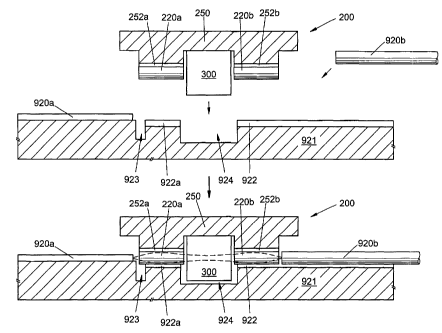
substrate
921 on a wafer scale, bar level, or individual chip level. The sizes of the
GRIN fiber
segments 220a and 220b, the V-groove 922 and V-groove segment 922a, the
optical component 300, and the recessed portion 924 are such that the V-groove
and V-groove segment mechanically engage the GRIN fiber segments before the
optical component has made contact with bottom or side surfaces of the
recessed
portion. Such engagement results in substantially coaxial optical alignment of
GRIN fiber segment 220a with planar waveguide 920a (within operationally
acceptable tolerances). Single-mode fiber 920b is positioned in V-groove 922,
resulting in substantially coaxial optical (and mechanical) alignment with
GRIN fiber
segment 220b (within operationally acceptable tolerances).
[0072] Waveguide substrate 921, optical assembly substrate 250, V-groove 922,
V-groove segment 922a, recessed portion 924, and/or optical component 300 may
be suitably adapted for enabling sufficiently accurate longitudinal
positioning of
optical assembly 200 and optical component 300 relative to the end of
waveguide
920a. Suitable adaptations may include, but are not limited to: alignment
edges
3o and/or other registering surfaces; interlocking surfaces; alignment marks
or targets;
kinematic alignment structures (such as grooves, recesses, protrusions, and
the
like); and so on. Alternatively, optical assembly 200 (and optical component
300)
may be pushed along the V-groove 922 and V-groove segment 922a to butt up
23
CA 02500053 2005-03-23
WO 2004/029669 PCT/US2003/027238
against the edge of slot 923, thereby reducing or substantially eliminating
variations
of longitudinal position of optical assembly 200 and optical component 300
relative
to the end of waveguide 920a. For longitudinal positioning of single mode
fiber
920b, alignment stops and/or alignment marks (none shown) may be formed within
or near the groove 922. The proximal end face of single mode fiber 920b may
butt
against corresponding alignment stops and/or be aligned with corresponding
alignment marks for sufficiently accurate longitudinal positioning relative to
the
respective GRIN fiber segment without making contact therewith. Alternatively,
the
proximal end face of single mode fiber 920b may butt directly against the
distal end
face of the corresponding GRIN fiber segment 220b for longitudinal
positioning.
[0073] Once properly positioned, optical assembly 200 (with optical component
300) and single mode optical fiber 920b may be secured to planar waveguide
substrate 921 by any suitable means, including but not limited to: adhesives;
embedding media (including encapsulants, polymers, and so forth); one or more
clamps, retainers, covers or lids, or other structural components; solder;
electrostatic interactions; heat/pressure bonding; and so forth. An index-
matching
embedding medium (such as a polymer, for example) may be employed between
the proximal end face(s) of planar waveguide 920a and/or single mode fiber
920b
and the distal end faces of respective GRIN fiber segments 220a and 220b, to
reduce or substantially eliminate unwanted reflections and increase overall
optical
throughput. Such an index-matching medium may have an index near or between
the indices of the GRIN fiber segments, the single mode fiber, and/or the
planar
waveguide, although any medium that reduces the reflectivity at the various
optical
surfaces could be employed. The index-matching embedding medium may be the
same as that employed (if any) between proximal end faces of the GRIN fiber
segments and the end faces of optical component 300, or may be a different
index
matching medium. The index-matching embedding medium may also serve to
secure the GRIN fiber segments and/or single-mode fiber within the V-groove
and/or V-groove segment. The index-matching embedding medium may be applied
selectively at the end faces and/or V-grooves, or may be employed as an
encapsulant 954 for optical component 300, GRIN lenses 220a and 220b, and
adjacent portions of planar waveguide 920a and single-mode fiber 920b (as in
Fig.
7C; encapsulant may also serve as a hermetic sealant). An index-matching
24
CA 02500053 2005-03-23
WO 2004/029669 PCT/US2003/027238
embedding medium or encapsulant may also function as a mechanical, moisture,
chemical, and/or hermetic protective barrier.
[0074] Spatially selective material processing employed for forming waveguide
920a, V-groove 922, and V-groove segment 922a enables sufficiently accurate
and
substantially reproducible/repeatable transverse and longitudinal alignment
between planar optical waveguide 920a, single-mode optical fiber 920b, and the
respective GRIN fiber segments 220a and 220b, as already described
hereinabove.
The optical modes are approximately indicated by the dashed lines in Figs. 7A
and
7B.
[0075] Dual-lens optical assemblies described thus far have involved
substantially
coaxial optical alignment of waveguides, fibers in V-grooves, fiber segments
in
V-grooves, and so forth. Such configurations may be appropriate in
circumstances
in which substantially normal incidence on optical component 300 is suitable
and/or
acceptable. However, in many instances substantially normal incidence on
optical
component 300 may lead to undesirable back-reflections, potentially degrading
the
performance of the optical system through unacceptably high levels of optical
feedback. This may be reduced by application of anti-reflection coatings
and/or
index-matching media, and/or by alignment of the optical component 300
somewhat away from normal incidence (typically by less than about 100, often
less
than about 5 , perhaps less than about 2 ; depends on geometry, mode
characteristics, sensitivity of upstream optical components to back-
reflections, and
so on). However, off-normal incidence also results in lateral displacement of
an
optical beam propagating through the optical component (up to a few tens of
microns for optical components ranging from several hundred microns up to a
few
millimeters long). Such lateral displacement would result in decreased
transmission through a dual-lens optical assembly as described herein if the
GRIN
fiber segments are substantially collinear. Therefore, additional embodiments
of
the optical assemblies disclosed herein may be constructed in which the GRIN
fiber
segments 220a and 220b are laterally displaced, and the corresponding V-groove
segments and/or waveguide(s) on a mating fiber/waveguide substrate or
waveguide substrate are similarly displaced. The optical assembly substrate
250
(including recessed area 251, saw cut 254, and/or recessed area 255, as the
case
may be) may be adapted for aligning the optical component 300 at a well-
CA 02500053 2005-03-23
WO 2004/029669 PCT/US2003/027238
characterized off-normal angle of incidence, enabling precise calculation of
the
resulting lateral displacement of a transmitted optical beam.
[0076] For forming laterally-displaced dual-lens optical assemblies analogous
to
the exemplary substantially collinear embodiments disclosed hereinabove, V-
groove(s) 252 may be formed on substrate 250 to comprise multiple longitudinal
segments, laterally displaced from one another by the calculated distance
(Fig. 10).
The calculated distance may be realized with the accuracy/precision
characteristic
of the spatially selective material processing employed therefor. Recessed
areas
(251 or 255, as the case may be) are formed between these laterally displaced
segments of the V-groove 252, regardless of whether cleaving or saw cuts are
to
be employed for dividing the GRIN fiber into segments. A length of GRIN fiber
220
is positioned and secured within the V-groove 252, curving over the recessed
areas
to accommodate the lateral displacement of the segments of the V-groove 252.
Upon dividing the GRIN fiber 220 into segments 220a and 220b (by cleaving, saw
cuts, or other method), the segments are laterally displaced by the same
distance
as the laterally displaced V-groove segments 252a and 252b. Optical power
collected by one of the GRIN fiber segments and transmitted through an off-
normal
optical component 300 positioned between the GRIN fiber segments is therefore
substantially centered on the other GRIN segment. Instead of spanning recessed
area 251 with a single GRIN optical fiber 220 (as shown in the first step of
Fig. 10),
separate segments of GRIN optical fiber may be positioned and secured with the
laterally displaced V-groove segments, and then cleaved or cut to the desired
length.
[0077] Fig. 11 shows an exemplary dual-lens optical assembly analogous to that
depicted in Figs. 5A-5C adapted for transferring optical power between two
optical
fibers 520a and 520b. Dashed lines indicating the optical modes are omitted.
The
embodiment of Fig. 11 differs from that of Figs. 5A-5C only in that the V-
groove
segments 252a/252b and 552a/552b are laterally displaced, so as to accommodate
an off-normal optical component 300. Spatially selective material processing
may
3o be employed for forming the various grooves/segments on substrate 250 in
the
proper positions. Figs. 12 and 13 show exemplary optical assemblies analogous
to
those depicted respectively in Figs. 6A-6C (adapted for transferring optical
power
between two planar waveguides) and 7A-7C (adapted from transferring optical
26
CA 02500053 2005-03-23
WO 2004/029669 PCT/US2003/027238
power between a planar waveguide and an optical fiber). Dashed lines
indicating
the optical modes are omitted. The embodiments of Figs. 12 and 13 differ from
their respective collinear analogues only in that the waveguides 720a/720b and
V-
groove segments 722a/722b (Fig. 12) and the waveguide/fiber 920a/920b and
V-groove/segment 922/922a (Fig. 13) are laterally displaced, so as to
accommodate an optical assembly 100 with substantially similarly displaced
GRIN
segments 220a/220b and an off-normal optical component 300. Spatially
selective
material processing may be employed for forming the various waveguide(s),
groove(s), and groove segment(s) on substrate 721 (Fig. 12) or 921 (Fig. 13)
in the
proper positions.
[0078] It should be noted that embodiments may be made that are analogous to
the exemplary embodiments of Figs. 10-13, except that the displacement of the
GRIN fiber segments is in the vertical dimension. Such embodiments fall within
the
scope of the present disclosure. Such vertical displacement may be achieved in
a
variety of suitable ways, including but not limited to the following examples.
Portions of V-groove 252 may be formed at different depths, so that the
resulting V-
groove segments 252a/252b and the GRIN fiber segments 220a/220b therein are
at different depths. Corresponding V-groove segments 552a/552b (if present)
would also be formed at different depths. V-groove segments 722a/722b on a
waveguide substrate 721, as well as waveguides 720a/720b, would be formed at
differing heights. V-groove segments 922a/922b, V-groove 922, and waveguide
920a would be formed on a waveguide substrate 921 at differing heights.
Optical
component 300, substrate 250, and/or substrate 721 or 921, would be adapted
for
providing off-normal faces tilted in the vertical direction.
[0079] It may be desirable in some instances of embodiments similar to those
of
Figs. 6A-6C, 7A-7C, 12, and 13 to position and align the optical component 300
on
the planar waveguide substrate (721 or 921), instead of on substrate 250 (with
the
GRIN segments 220a and 220b). Since transverse positioning of the optical
component 300 typically does not require a high degree of accuracy, it may not
be
necessary to include the optical component 300 in an optical assembly with the
GRIN fiber segments. Exemplary assembly procedures are illustrated in Figs. 14
and 15, wherein the optical component 300 is positioned and aligned on
waveguide
substrate 721 or 921 (the waveguide substrate being adapted therefor;
adaptations
27
CA 02500053 2005-03-23
WO 2004/029669 PCT/US2003/027238
not shown), and then an optical assembly as variously described hereinabove
(minus the optical component 300 but including V-groove-mounted GRIN segments
220a/220b) is then positioned and aligned on substrate 721 or 921. Dashed
lines
indicating the optical modes are omitted.
[0080] It may be desirable in various disclosed embodiments to position each
of
the GRIN segments 220a/220b individually on waveguide substrate 721 or 921, or
on a second substrate with optical fibers 520a and 520b. Instead of forming
dual-
lens optical assemblies, the substrate wafer 250 is divided into individual
lens
substrates 250a or 250b, each having thereon only one GRIN segment 220a or
220b in a corresponding V-groove segment 252a/252b (Fig. 16). GRIN segments
220a and 220b thus formed may be substantially identical, or may differ in
length.
One or more of these single GRIN lens substrates may be assembled onto a
waveguide substrate 721 or 921 (adapted in any of the ways variously set forth
hereinabove) along with an optical component 300 as shown in Figs. 17 and 18.
Dashed lines indicating the optical modes are omitted. Separate mounting of
the
two GRIN lens segments may be used to implement any dual-lens embodiment set
forth herein or falling within the scope of the present disclosure. Embedding
and/or
index-matching media or encapsulant(s) may be employed, as described above.
Alignment and securing of GRIN fiber segments to the substrate may be
accomplished as described hereinabove. If GRIN segments arising from adjacent
portions of a common GRIN fiber are used, axial asymmetry of the GRIN fiber is
self-correlated, as with the dual-lens assemblies described hereinabove.
Alternatively, use of separate GRIN segments enables use of differing GRIN
profiles in a two-lens optical device, adding another design parameter for
implementing such two-lens optical devices.
[0081] There may be instances in which a single lens may provide an adequate
(i.e., operationally acceptable) level of optical power transfer between
fiber(s)
and/or waveguide(s). In such cases a single GRIN segment mounted on its own
substrate (as in Figs. 16-18) may be assembled with other optical components
in a
manner to that already described hereinabove. Exemplary single-lens
embodiments are shown in Figs. 27-29, and fall within the scope of the present
disclosure and/or appended claims.
28
CA 02500053 2005-03-23
WO 2004/029669 PCT/US2003/027238
[0082] Various structural adaptations of optical assemblies disclosed herein
may
be required depending on the intended alignment configuration. Similarly,
fabrication and/or assembly procedures may require modifications depending on
the alignment configuration to be employed. In particular, the manner in which
GRIN optical fiber 220 is secured to substrate 250 during and after forming
GRIN
fiber segments 220a and 220b may vary depending on the subsequent assembly
and/or use of the optical assembly. Any suitable method may be employed for
securing the GRIN fiber 220 once it is positioned in V-groove 252, and for
holding it
in place as the fiber is divided into GRIN fiber segments 220a and 220b, by
cleaving, saw cuts, and/or other suitable technique. Suitable methods may
include
but are not limited to: adhesives; embedding media (including encapsulants,
polymers, and so forth); one or more clamps, retainers, covers or lids, or
other
structural components; solder; electrostatic interactions; heat/pressure
bonding;
and so forth. Such methods may be similarly employed for securing GRIN fiber
segments of an optical assembly into V-groove segments on a planar waveguide
substrate (as in Figs. 6A-6C and 7A-7C, for example), or for securing optical
fiber(s) onto a substrate along with the GRIN segments (as in Figs. 5A-5C, for
example).
[0083] Some of these techniques for securing GRIN optical fiber 220 in V-
groove
252 may rely on the presence of metal. A metal-coated GRIN optical fiber may
be
secured within a V-groove using solder, for example. Such solder may be
spatially-
selectively applied to the substrate 250 and/or V-groove 252, and may be
bonded
to a metal coating of a GRIN optical fiber. Solder reflow may enable
sufficiently
accurate positioning of the GRIN optical fiber engaged with the V-groove.
Another
technique relying on the presence of metal is heat/pressure bonding of glass
and/or
silicon with aluminum (or perhaps an oxide coating thereof; the exact
mechanism is
not known). Mechanical bonding of convex surfaces to flat surfaces, wherein
one
surface is silica or silicon and the other surface is aluminum, has been
previously
disclosed in U. S. Pat. No. 5,178,319 to Coucoulas and U. S. Pat. No.
5,389,193 to
Coucoulas et al. Aluminum coatings maybe applied to substrates and/or optical
fibers with accurately known thicknesses, and the heat/pressure bonding
results in
no substantial deformation of the substrate, fiber, or coating. Heat/pressure
bonding therefore may be employed while maintaining sufficiently accurate
29
CA 02500053 2005-03-23
WO 2004/029669 PCT/US2003/027238
positioning of fibers/segments within V-grooves, for example. Substrates 250,
721,
and/or 921 may comprise silicon substrates, while GRIN fiber 220 may be silica
or
silica-based.
[0084] In one heat/pressure technique, the GRIN optical fiber may be provided
with an aluminum coating, ranging in thickness from a few microns up to a few
tens
of microns, typically around 10 microns thick. By applying pressure and heat
(or
acoustic energy) to the aluminized GRIN fiber within the V-groove (in silicon
substrate 250), a robust mechanical bond is formed between the fiber and the V-
groove. Pressure, heat, and/or acoustic energy may be applied along
substantially
the entire length of GRIN fiber 220 within V-groove 252, or may be applied in
a
localized fashion only to those fiber/ V-groove segments where a GRIN fiber
segment is ultimately desired. After the optical assembly is formed (as in the
exemplary procedures of Figs. 3A-3C, Figs. 3D-3F, Fig. 10, or Fig. 16, with
the
GRIN segments held in place by the silicon/aluminum bond; aluminum coatings
not
shown), heat/pressure bonding may be further employed to assemble it with a
silicon planar waveguide substrate (as in exemplary procedures of Figs. 6A-6C,
Figs. 7A-7C, Figs. 12-15, Figs. 17-18, or Figs. 27-29; aluminum coatings not
shown). The aluminized GRIN segments may be bonded to the V-grooves of the
waveguide substrate by additional application of pressure and heat (or
acoustic
energy). Since the V-grooves provide both lateral as well as (with the GRIN
fiber
diameter) vertical alignment, the additional size of the GRIN fiber added by
the
presence of the aluminum coating must be accounted for in designing the V-
grooves and waveguides on the waveguide substrate (721 or 921). Similarly, for
fabricating an embodiment analogous to the examples of Figs. 5A-5C and Fig.
11,
aluminized optical fiber (having substantially the same diameter) may be used
for
fibers 520a/520b as well as the GRIN segments. Alternatively, if non-
metallized
optical fiber is used for fibers 520a and/or 520b, then V-groove segments
252a/252b and 552a/552b must be made of suitably differing depths, to achieve
an
acceptable degree of vertical alignment between the GRIN segments and optical
fibers.
[0085] In another heat/pressure technique, non-metallized optical fiber is
employed, and a coating of aluminum may be applied to at least portions of V-
groove 252. A silica or silica-based GRIN optical fiber 220 pressed into such
an
CA 02500053 2005-03-23
WO 2004/029669 PCT/US2003/027238
aluminized V-groove will form a robust mechanical bond upon application of
heat or
acoustic energy. It may be desirable to provide the aluminum coating to only
those
portions of the V-groove 252 where a GRIN fiber segment is ultimately desired.
Alternatively, pressure, heat, and/or acoustic energy may be applied in a
localized
fashion only to those fiberN-groove segments where a GRIN fiber segment is
ultimately desired. Alternatively, substantially the entire V-groove may be
aluminized for heat/pressure bonding of GRIN optical fiber 220. Forming
recessed
areas 251/253a/253b as in Figs. 3A-3C or making saw cuts 254/256a/256b as in
Figs. 3D-3F (as the case may be) to divide V-groove 252 into V-groove segments
252a/252b also serves to remove the aluminum coating and V-groove from regions
where it is not needed or desired. After the optical assembly is formed (as in
the
exemplary procedures of Figs. 3A-3C, Figs. 3D-3F, Fig. 10, or Fig. 16, with
the
GRIN segments held in place by the silicon/aluminum bond; aluminum coatings
not
shown), heat/pressure bonding may be further employed to assemble it with a
silicon planar waveguide substrate (as in the exemplary procedures of Figs. 6A-
6C,
Figs. 7A-7C, Figs. 12-15, Figs.17-18, or Figs. 27-29; aluminum coatings not
shown). The V-groove segments on the waveguide substrate that engage the
GRIN segments may be aluminized, and the GRIN fiber segments of the optical
assembly bonded to the V-grooves of the waveguide substrate by additional
application of pressure and heat (or acoustic energy). Since the V-grooves
provide
both lateral as well as (with the GRIN fiber diameter) vertical alignment, the
thickness of the aluminum coating must be accounted for in designing the V-
grooves and waveguides on the waveguide substrate (721 or 921). Similarly, for
fabricating an embodiment analogous to the examples of Figs. 5A-5C and Fig.
11,
the thickness of the aluminum coating in V-groove segments 220a/220b must be
accounted for. This may be accomplished by providing an aluminum coating of
substantially the same thickness in V-groove segments 552a/552b, by using
optical
fibers 520a/520b of suitably differing diameter from the GRIN fiber segment
diameters, or by forming V-groove segments 252a/252b and 552a/552b at suitably
3o differing depths, to achieve an acceptable degree of vertical alignment
between the
GRIN segments and optical fibers.
[0086] In other exemplary embodiments of optical assemblies and fabrication
thereof as disclosed herein, adhesives or polymers may be employed for
securing
31
CA 02500053 2005-03-23
WO 2004/029669 PCT/US2003/027238
GRIN fiber 220 within V-groove 252 during and after forming GRIN fiber
segments
220a/220b. Such an adhesive or polymer (these terms shall be used
interchangeably hereinbelow) may be substantially uniformly applied over the
substrate wafer. Such an adhesive or polymer may instead be: spatially
selectively
applied; substantially uniformly applied and spatially selectively removed
(before or
after curing); or substantially uniformly applied and spatially selectively
cured, to
facilitate subsequent processing and assembly of the optical component 300
with
the optical assembly 200, and to facilitate positioning, alignment, and
securing of
the optical assembly 200 relative to other planar waveguide(s) and/or optical
fiber(s). For example, adhesive or polymer may be required to hold GRIN fiber
220
during cutting and/or to retain GRIN fiber segments 220a and 220b properly
aligned
in V-groove segments 252a and 252b. However, any cured adhesive or polymer
should be substantially absent from V-groove segments 552a and 552b on
substrate 250, in order to enable accurate alignment of single mode fibers
520a
and 520b positioned therein (as in Figs. 5A-5C or Fig. 11). In another
example, any
cured adhesive or polymer should be substantially absent from at least a
portion of
each of GRIN fiber segments 220a and 220b to enable accurate alignment of the
optical assembly 200 with GRIN segments 220a and 220b engaged with a
waveguide substrate V-groove or segment thereof (as in Figs. 6A-6C, Figs. 7A-
7C,
Figs. 12-15, Figs. 17-18, or Figs. 27-29).
[0087] Optical assemblies 200 suitable for use as illustrated in Figs. 5A-5C
or Fig.
11 may be fabricated according to the exemplary procedure illustrated in Figs.
8A-
8B. A substantially similar procedure may be implemented for fabricating
assemblies on a wafer scale, at the bar level, or for fabricating individual
optical
assemblies. A polymer layer is applied in strips 560 substantially
perpendicular to
V-grooves 252 and GRIN fibers 220 positioned therein, thereby leaving
intervening
segments of V-grooves 252 substantially free of polymer. Saw cuts 254 are made
through a central portion of the polymer strips 560, while saw cuts 256a and
256b
are made along the edges of polymer strips 560. Saw cuts 256a and 256b thus
positioned allow GRIN fiber segments in the intervening portion of V-groove
252
(the portions substantially lacking polymer coverage) to be removed therefrom.
The substrate wafer is divided between adjacent saw cuts 256a and 256b to form
individual optical assemblies 200, leaving empty V-groove segments 552a and
32
CA 02500053 2005-03-23
WO 2004/029669 PCT/US2003/027238
552b on each assembly substrate 250 adjacent each GRIN fiber segments 220a
and 220b. The optical assembly thus formed is thereby prepared for receiving
single mode fibers 520a and 520b, as in Figs. 5A-5C. Polymer 560 substantially
completely covers lateral surfaces of GRIN fiber segments 220a and 220b, and
holds the GRIN fiber segments within V-groove segments 252a and 252b. If
additional processing of the optical assembly is needed or desired, polymer
560
may serve as a mask protecting lateral surfaces of GRIN fiber segments 220 and
220b from such processing steps. For example, a wet etch might be employed to
improve the optical quality of the transmissive end surfaces of GRIN fiber
segments
220a and 220b (improve the optical quality relative to that left by the saw
cut
process), and polymer 560 protects the lateral surfaces of the GRIN fiber
segments
from the wet etch. In such a case, the it may be desirable to apply at least
some of
the polymer (precursor) prior to placement of GRIN fiber 220, to ensure that
the
underside of the GRIN fiber segments (within the V-groove segments) are
protected as well. Any embedding medium and/or index matching medium or
encapsulant employed with optical component 300 and/or single-mode fibers 520a
and 520b (as in Fig. 5C) may also surround polymer 560.
[0088] Optical assemblies 200 suitable for use as illustrated in Figs. 6A-6C,
Figs.
7A-7C, Figs. 12-15, Figs. 17-18, or Figs. 27-29 may be fabricated according to
the
exemplary procedure illustrated in Figs. 9A-9B. A substantially similar
procedure
may be implemented for fabricating assemblies on a wafer scale, at the bar
level,
or for fabricating individual optical assemblies. A polymer layer is provided
as sets
of three strips 754/756a/756b substantially perpendicular to V-grooves 252 and
GRIN fibers 220 positioned therein. Polymer strips 754/756a/756b are
positioned
to correspond roughly to the positions of saw cuts 254/256a/256b, and the
intervening segments of GRIN optical fiber 252 are substantially free of
polymer.
Polymer strip 754 is wider than saw cut 254, which divides polymer strip 754
into
polymer strip segments 754a and 754b. Polymer strips 756a and 756b are
positioned so that portions of their respective outer edges are removed by saw
cuts
256a and 256b. As a result, GRIN fiber segment 220a is secured within V-groove
segment 252a by a polymer strip 754a at its inner (i.e., proximal) end and
polymer
strip 756a at its outer (i.e., distal) end, leaving a central portion of the
GRIN fiber
segment substantially free of polymer. GRIN fiber segment 220b is similarly
33
CA 02500053 2005-03-23
WO 2004/029669 PCT/US2003/027238
secured within V-groove segment 252b by a polymer strip 754b at its inner end
and
polymer strip 756b at its outer end, leaving a central portion of the GRIN
fiber
segment substantially free of polymer. The substrate wafer is divided between
adjacent saw cuts 256a and 256b to form individual optical assemblies 200. If
additional processing is needed or desired (such as a wet etch to improve
optical
quality of GRIN fiber segment transmissive end surfaces, as described
hereinabove), a temporary mask (not shown) may be employed, if needed, to
protect the exposed lateral surfaces of the GRIN fiber segments. Such a
temporary
mask is typically selectively removable from the GRIN fiber segments while
leaving
polymer strips 754/756a/756b intact.
[0089] The substantially polymer-free central portions of the GRIN fiber
segments
facilitate accurate vertical alignment of the GRIN fiber segments within V-
grooves
and/or V-groove segments on the waveguide substrate. The polymer strips
756a/756b may be received within slots in the waveguide substrate (to enable
engagement of the GRIN fiber segments with the waveguide substrate V-groove;
slots 723a/723b in Figs. 6A-6C; slot 923 in Figs. 7A-7C along with an
additional slot
not shown). The polymer strip segments 754a/754b may be similarly received
within a recessed portion of the waveguide substrate along with optical
component
300 (recessed portion 724 in Figs. 6A-6C; recessed portion 924 in Figs. 7A-
7C).
One or more of polymer strips 754a/754b/756a/756b may engage a substrate for
facilitating longitudinal alignment of the GRIN segment(s). An optical
assembly
thus formed may be employed between two planar optical waveguides (as in Figs.
6A-6C, Fig. 12, Fig. 14, Fig. 17, or Fig. 27) or between a planar optical
waveguide
and a single-mode optical fiber (as in Figs. 7A-7C, Fig. 13, Fig, 15, Fig. 18,
Fig. 28,
or Fig. 29). Any embedding medium and/or index matching medium or encapsulant
employed with optical component 300, planar waveguide(s), and/or a single-mode
fiber may also surround polymer strips 754a/754b/756a/756b.
[0090] Another exemplary procedure for forming optical assembly 200 which
would leave portions of GRIN fiber segments substantially free of cured
polymer is
shown in Fig. 19. A substantially uniform polymer or adhesive layer 999 is
deposited on substrate wafer 250, which includes V-groove(s) 252. GRIN optical
fiber(s) 220 are positioned in V-groove(s) 252, and the polymer or adhesive is
cured. The polymer layer 999 is sufficiently thin that when GRIN optical
fibers are
34
CA 02500053 2005-03-23
WO 2004/029669 PCT/US2003/027238
placed in the polymer layer and positioned in the V-groove(s), the polymer
leaves a
significant portion of the circumference of the GRIN fiber uncovered. The
uncovered portion of the circumference is large enough to allow it to engage
the
corresponding V-groove on a waveguide substrate upon assembly therewith. Saw
cuts 254 (shown in Fig. 19) and 256a/256b (not shown in Fig. 19) are made as
described hereinabove, optical component 300 positioned and the substrate
wafer
divided into individual assembly substrates, and the resulting optical
assemblies
assembled onto V-grooves of corresponding waveguide substrates (as in Figs 6A-
6C and 7A-7C). The success of this technique may depend on the viscosity
and/or
wetting properties of the polymer before curing, which may facilitate or
render
problematic the placement of the GRIN fiber while maintaining a portion of its
circumference substantially free of polymer.
[0091] It should be understood that any of the techniques described herein for
forming a dual-GRIN-lens assembly may be suitably adapted for forming single-
GRIN-segment assembly (i.e., a GRIN segment mounted on its own substrate, as
in Figs. 16-18 and 27-29), and that such adaptations fall within the scope of
the
present disclosure and/or appended claims.
[0092] It should be understood that optical propagation through any of the
optical
assemblies disclosed herein may occur in either or both directions. In
particular, in
the exemplary embodiments of Figs. 7A-7C, Fig. 13, Fig. 15, Fig. 18, and Figs.
28-
29, optical power may propagate from planar waveguide 920a, through optical
assembly 200 and optical component 300, and into single-mode optical fiber
920b,
and also from single-mode optical fiber 920b, through optical assembly 200 and
optical component 300, and into planar waveguide 920a. It should be understood
that while exemplary embodiments have been disclosed including optical
assemblies used with single-mode optical fiber, the optical assemblies
disclosed
herein may also be adapted for and used with multi-mode optical fiber,
expanded-
mode optical fiber, and other types of optical fiber. Similarly, planar
waveguides
used with the disclosed optical assemblies may be single-mode, multi-mode,
expanded-mode, and so forth. Such uses of the disclosed optical assemblies
with
various types of optical fibers and/or planar waveguides shall nevertheless
fall
within the scope of the present disclosure and/or appended claims.
CA 02500053 2005-03-23
WO 2004/029669 PCT/US2003/027238
[0093] In addition to the example of an optical isolator as optical component
300, a
dual-lens optical assembly 200 as disclosed herein may be implemented for
placement and alignment of any one or more suitable "free-space" optical
component(s) 300 between GRIN fiber segments 220a and 220b. Such
components may include, but are not limited to: polarization-dependent and/or
polarization-independent optical isolators; thin-film filters; bulk
polarizers,
polarization rotators, waveplates, birefringent wedges, analyzers, and/or
other
polarization components; micro-mirrors and/or micro-beamsplitters; optical
taps;
diffractive optics; and so forth. A portion of the functionality of any free-
space
1o optical component 300 (incorporated into an optical assembly according to
the
present disclosure) may reside in a planar waveguides 720a and/or 720b (Figs.
6A-
6C, Fig. 12, Fig. 14, Fig. 17, Fig. 27) or waveguide 920a (Figs. 7A-7C, Fig.
13, Fig.
15, Fig. 18, and Figs. 28-29). Such waveguide-based functionality may be
implemented on a wafer-scale for many waveguides concurrently, and may
potentially reduce the size and/or cost of the component 300 and/or the size
of the
gap required between the planar waveguide(s) and/or optical fiber, as well as
potentially reducing the overall manufacturing cost of the finished optical
assemblies. In one example of such inclusion of functionality in a waveguide,
one
linear polarizer may be omitted from a conventional optical isolator
(potentially
2o reducing its length). The required linear polarization selectivity may
instead be
incorporated into the planar waveguide on the substrate (by any suitable
means).
[0094] In addition to GRIN optical fiber for forming GRIN fiber segments
220a/220b, other gradient-index optical media, such as GRIN rods, may be
employed for forming functionally equivalent lens-like components as part of
optical
assemblies disclosed herein. Use of such alternative GRIN optical media shall
nevertheless fall within the scope of the present disclosure and/or appended
claims.
[0095] Figs. 20A and 20B illustrate another exemplary optical assembly. A
planar
waveguide 1120 is provided on a waveguide substrate 1102. Waveguide 1120
may be provided at its proximal end with a mode-expander segment 1122. The
mode expander is preferably arranged so as to provide substantially adiabatic
mode expansion, i.e., longitudinal variation of waveguide dimensions and/or
properties are sufficiently gradual so that only an operationally acceptable
fraction
36
CA 02500053 2005-03-23
WO 2004/029669 PCT/US2003/027238
of propagating optical power is lost by transfer into undesired modes. Optical
power propagating through waveguide 1120 and mode expander 1122 exits
through an end-facet of the waveguide/mode expander and diverges by so-called
free-space diffraction, determined primarily by the wavelength and the mode
characteristics at the end facet of the waveguide. The optical power then
enters an
entrance face of an optical component 1140 (such as an optical isolator, for
example) and propagates therethrough. The transverse dimensions of the optical
isolator are typically too large to provide substantial lateral confinement of
the
propagating optical power, which therefore continues to diverge through the
isolator. After exiting the isolator, the still-diverging optical power enters
a proximal
end face of an optical fiber 1170. Optical fiber 1170 preferably comprises a
single-
mode optical fiber provided at its proximal end with a short segment of multi-
mode
GRIN optical fiber, which acts as a focusing element 1172 (equivalently, as an
expanded-mode coupling segment), and serves to "collect" the diverging optical
power exiting the optical component 1140 and couple a substantial portion of
the
optical power into the single-mode fiber 1170. The length of the segment 1172
is
preferably selected so as to substantially spatially mode match the diverging
optical
power entering segment 1172 and the mode supported by single-mode optical
fiber
1170 (described further hereinbelow).
[0096] The exemplary optical assembly of Figs. 20A and 20B may be modified in
a
variety of ways for achieving a variety of performance requirements and/or
optimizing a variety of performance characteristics. The divergence of the
optical
mode emerging from the exit face of waveguide 1120 may be selected by suitable
design of mode-expander 1122. For example, if optical component 1140 is
relatively long (greater than about 0.5 mm, for example; isolators with
cemented
Polarcor or other bulk polarizers may typically exceed this length), it may
be
desirable to design mode expander 1122 to provide a larger mode size at the
waveguide exit face (and therefore correspondingly smaller mode divergence).
Mode sizes greater than about 10 gm up to several tens of gm across may be
3o desirable. On the other hand, an exiting mode size of less than about 10 pm
may
be desirable for enabling direct end-transfer of optical power between
waveguide/mode expander 1120/1122 and a single mode optical fiber (butt-
coupling or end-coupling), without an expanded-mode coupling fiber segment
37
CA 02500053 2005-03-23
WO 2004/029669 PCT/US2003/027238
and/or without the intervening optical component. This may be the case when a
common planar waveguide substrate 1102 is to be manufactured (with one or more
waveguides thereon) that may be used for optical assemblies either including
(Fig.
21A) or not including (Fig. 21 B) an optical component 1140 (with a single-
mode
optical fiber in groove 1107 and pushed forward near waveguide 1120 when
component 1140 is not present, with or without an expanded-mode coupling
segment 1172; shown without segment 1172 in Fig. 21 B). The smaller exiting
mode size and correspondingly larger divergence may limit the length of an
isolator
that may be used (to perhaps less than about 0.5 mm long; isolators with thin-
film
polarizer coatings applied thereto may fall within this length range), may
result in
over-filling of the input face of optical fiber 1170, and/or may require a
suitably
adapted focusing element or expanded-mode coupling segment 1172 for optical
fiber 1170 for optimizing optical power transfer into the single-mode fiber
(discussed further below). On the other hand, decreased optical power
transmission through the optical assembly (due to the larger divergence and
possible over-filling of the fiber input face) may be an operationally
acceptable
consequence of such a "dual-use" substrate (Fig. 21 A).
[0097] Waveguide 1120 and beam expander 1122 may be implemented in a
variety of ways. Waveguide 1120 may typically include a core and lower-index
cladding. The core may gradually taper (in one or both transverse dimensions)
along the length of the waveguide until it eventually terminates, leaving only
the
cladding to function as an air-guided ridge waveguide. Alternatively, the core
may
taper (either decreasing or increasing in one or both transverse dimensions)
without
terminating to yield a desired expanded mode size. In another suitable
configuration, a core/cladding waveguide may be embedded in another medium or
encapsulant having a lower index than the cladding. As the core gradually
tapers
away, the cladding begins to act as a waveguide core, while the embedding
medium or encapsulant acts as cladding. Myriad other suitable configurations
may
be contrived while remaining within the scope of the present invention, some
of
which are disclosed in above-cited App. No. 60/466,799. If the tapering and/or
termination of the core are substantially adiabatic, then the core-guided mode
will
smoothly evolve into a larger mode supported by the waveguide (an air-guided
mode in a ridge waveguide, for example). The spatial mode characteristics of
the
38
CA 02500053 2005-03-23
WO 2004/029669 PCT/US2003/027238
core-guided mode (and therefore the configuration, parameters, and dimensions
of
the core/cladding) are typically dictated by upstream optical
devices/components
coupled to and/or incorporated into the waveguide 1120. The spatial mode
characteristics of the expanded optical mode (and therefore the configuration,
parameters, and dimensions of the mode expander) are determined by the
considerations discussed in the preceding paragraphs. In one of many possible
implementations of the present invention, a silica-based waveguide 1120 may
include a silicon nitride or silicon oxynitride core, the core being several
pm wide
and only a few hundred nm thick or less. Such a thin-core waveguide may be
well-
suited for transverse-transfer of optical power, as described in U.S. App.
Nos.
60/334,705, 60/360,261, and 10/187,030, which may be useful for upstream
optical
power transfer into waveguide 1120 for propagation therethrough.
Alternatively, a
thin core waveguide of this type may enable spatial-mode-matched end-transfer
of
optical power with various other waveguides and/or devices. The width of the
thin
core may decrease along the mode-expander segment 1122 with the core
eventually terminating, leaving a larger doped silica core within the
cladding, or
leaving only silica-based cladding material to act as an air-guided ridge
waveguide
or as a waveguide core within a lower-index embedding medium or encapsulant.
Sufficiently gradual tapering and termination of the thin core results in
substantially
adiabatic evolution of the core-guided optical mode into an expanded optical
mode.
It should be noted that in some implementations of the present invention, a
mode
expander 1122 may be completely omitted, so that the optical mode supported by
waveguide 1120 simply exits the waveguide and propagates therefrom.
(0098] Many other types and/or configurations of planar waveguides may be
equivalently employed for implementing embodiments set forth herein and/or
equivalents thereof. These may include ridge waveguides, buried waveguides,
semiconductor waveguides, other high-index waveguides, silica-based
waveguides,
polymer waveguides, other low-index waveguides, core/clad type waveguides,
multi-layer reflector waveguides, metal-clad waveguides, air-guided
waveguides,
photonic crystal-based or photonic bandgap-based waveguides, and myriad other
examples not explicitly set forth herein but that may nevertheless fall within
the
scope of inventive concepts disclosed and/or claimed herein. In any of these
examples, substantially adiabatic variation of one or more of the material(s),
39
CA 02500053 2005-03-23
WO 2004/029669 PCT/US2003/027238
configuration, parameters, and/or dimensions of the waveguide may be employed
for producing an expanded optical mode exiting the mode expander with the
desired divergence characteristics. It should be noted that a planar waveguide
mode expander as described herein may be formed at the proximal ends of planar
waveguides 720a and/or 720b (in the exemplary embodiments of Figs. 6A-6C, Fig.
12, Fig. 14, Fig. 17, or Fig. 27) or planar waveguide 920a (in the exemplary
embodiments of Figs. 7A-7C, Fig. 13, Fig, 15, Fig. 18, Fig. 28, or Fig. 29).
(0099] Optical fiber 1170 with expanded-mode coupling segment 1172
(equivalently, collecting segment or focusing segment) may include a single-
mode
optical fiber and a short segment of multi-mode optical fiber coupled to its
end to
serve as a focusing or collecting element (functionally similar to GRIN
segment(s)
220a and/or 220b of Figs. 5A-5C or Fig. 11, or to GRIN segment 220b of Figs.
7A-
7C, Fig. 13, Fig. 15, or Fig. 18, for example). The index profile of the multi-
mode
fiber and the length of the segment 1172 may be tailored to optimally couple a
freely-propagating optical mode and the mode of single-mode fiber 1170 fused
to
segment 1172. The multi-mode fiber segment may be secured to the single-mode
fiber for end-transfer of optical power (i.e., butt-coupling'or end-coupliing)
by-,a
variety of means, preferably by fusion splicing of the multi-mode GRIN.,fiber
segment to the single-mode fiber, or alternatively by cementing or by,a
ferrule'.or
other similar mechanical device. Relative concentricity' of the multi mode
fiber
segment and the single-mode fiber is desirable, and may be
readily"achiev6&159'
fusion splicing of fibers having substantially similar outer diameters.
Gradient-index
multi-mode fiber having various core diameters, cladding diameters, and/or
index
gradients are available commercially, and may be selected for satisfying
specific
performance requirements for mode-expanded coupling segment 1172. In
particular, GRIN optical fiber having an outer cladding diameter of about 125
m is
well-suited for substantially co-axial fusion to standard single-mode optical
fiber
(which also typically has an outer cladding diameter of about 125 m). Quarter-
pitch lengths for available GRIN optical fiber are on the order of 0.2 mm to 2
mm,
3o and segments may be cleaved or polished to a design length with accuracy of
a few
microns for achieving desire focusing properties.
[0100] A single-mode optical fiber 1170 with an expanded-mode coupling segment
1172 may be substantially coaxially positioned with respect to waveguide 1120
and
CA 02500053 2005-03-23
WO 2004/029669 PCT/US2003/027238
the mode-expander 1122 thereof, leaving a gap between them for accommodating
optical component 1140 (an optical isolator, for example). The mode expander
1122 and expanded-mode coupling segment 1172 may be suitably adapted (as
described in the preceding paragraphs) so as to achieve an optimal level of
optical
power transfer therebetween for a particular longitudinal spacing.
Alternatively,
mode expander 1122 and expanded-mode coupling segment 1172 may be suitably
adapted so as to achieve an operationally acceptable level of optical power
transfer
therebetween over a range of longitudinal spacings (which may include no gap,
i.e.,
butt-coupling of the waveguide 1120 and fiber 1170). The longitudinal spacing
(or
range thereof) may be determined by the size (or range of sizes) of component
1140 that may be placed between waveguide 1120 and fiber 1170.
[0101] It may be desirable to provide waveguide 1120 with an expanded-mode
coupling segment 1122 having performance (i.e., focusing properties) similar
to
segment 1172. As shown in Figs. 22A and 22B, waveguide 1120 may terminate
with a segment 1122 with an enlarged core (including an index gradient;
parameters determined by requirements for propagating through the isolator and
into the optical fiber), which would function in a manner analogous to GRIN
fiber
segment 1172 coupled to single-mode fiber 1170. Waveguide segment 1122 may
be configured slightly longer than the corresponding quarter-pitch length,
thereby
providing a collimated or slightly convergent optical mode for propagation
through
isolator 1140. This may enable use of a longer optical component 1140, since
the
divergent portion of the optical mode entering segment 1172 will be shifted
farther
from the exit face of segment 1122.
[0102] Transverse and/or angular alignment of waveguide 1120 and fiber 1170
significantly affects the degree of optical power transfer that may be
achieved
therebetween. Use of a planar waveguide on a substrate may facilitate
transverse
alignment, and may enable passive assembly of waveguide, isolator, and optical
fiber while achieving operationally acceptable levels of optical power
transfer
through the optical assembly. In particular, fabrication of alignment
structures on
the waveguide substrate (for later positioning of the optical component and
the
optical fiber) substantially concurrently with fabrication of the waveguide
1120 and
mode expander 1122 (if present), using spatially-selective fabrication
techniques,
ensures accurate relative positioning of the alignment structures relative to
the
41
CA 02500053 2005-03-23
WO 2004/029669 PCT/US2003/027238
waveguide/mode expander. In turn, these alignment structures (grooves, V-
grooves, pockets, edges, risers, posts, and so on, which may be very
accurately
formed on a silicon PLC substrate using standard lithography techniques, for
example), enable accurate placement of the optical component 1140 and optical
fiber/expanded-mode coupling segment 1170/1172 on substrate 1102 relative to
waveguide/mode expander 1120/1122. Sub-micron accuracy is readily achieved
using standard lithographic techniques on a silicon substrate, for example.
Figs.
20A/20B, 21A/21B, and 22A/22B show a groove 1104 for receiving and positioning
optical component 1140, and a V-groove 1107 for receiving optical
fiber/focusing
segment 1170/1172. Groove 1104 may be slightly over-sized (for tolerance
purposes), and may be fabricated so that one edge provides the required
longitudinal and/or angular alignment of component 1140. End faces of isolator
1140 may typically be oriented substantially normal to a propagation axis
defined
by waveguide 1120 and fiber 1170/groove 1107, or a non-normal angle of
incidence on component 1140 may be desirable for a variety of reasons; in
either
case the orientation of at least one edge of, groove 1104 provides the
necessary
alignment guide.
[0103] Other structures, waveguides, devices, and so forth may also be
fabricated
on substrate 1102 substantially concurrently with the waveguide/mode expander
and alignment structures, for forming multi-component optical devices and/or
assemblies. Furthermore, these spatially-selective fabrication techniques may
typically be implemented on a wafer scale for many devices simultaneously
(hundreds or even thousands of devices on a single wafer). Passive
assembly/alignment and wafer-scale processing each contribute significantly
for
enabling substantial economies-of-scale to be realized for the fabrication and
assembly of finished optical assemblies and/or devices.
[0104] An optical assembly according to the present invention may be employed
for providing an "in-line" optical isolator for an optical fiber (Figs. 23A
and 23B). A
PLC or other planar waveguide 1120 on a waveguide substrate 1102 may be
provided with an distal end adapted for substantially spatial-mode-matched end-
transfer of optical power with a single-mode optical fiber 1110. A V-groove
1101
may be provided in the waveguide substrate 1102 for receiving and aligning the
optical fiber 1110 relative to the waveguide 1120. Optical power propagating
42
CA 02500053 2005-03-23
WO 2004/029669 PCT/US2003/027238
through the waveguide diverges from its proximal end face. The proximal end of
the waveguide 1120 may be suitably adapted for achieving desired divergence
properties for the exiting optical power (with mode expander 1122, for
example),
which then enters the optical component 1140 and propagates therethrough
(still
diverging). The optical component 1140 may be received in and positioned by an
alignment groove 1104 provided in the waveguide substrate 1102. A V-groove
1107 is provided in the waveguide substrate 1102 for receiving an optical
fiber 1170
and aligning it with the waveguide 1120. The proximal end of the optical fiber
1170
may include an expanded-mode coupling segment 1172 (i.e., a focusing segment
comprising a GRIN optical fiber segment fusion-spliced or otherwise joined to
the
single-mode optical fiber 1170) as described hereinabove, suitably adapted for
collecting optical power transmitted through the component 1140 and coupling
it
into the mode supported by the optical fiber 1170. Wafer-scale fabrication of
many
waveguides substantially concurrently with the grooves, V-grooves, and any
other
required alignment structures may ensure operationally acceptable optical
power
throughput for passively assembled and aligned devices (while also reducing
manufacturing costs). Additional components may be implemented on the
waveguide substrate (on a wafer scale) for producing high-performance
isolators,
such as optical tap(s), optical detector(s) for monitoring power, thermo-optic
compensator element(s), electro-optic element(s), and so on. Feedback and/or
control "circuitry may be employed for stabilizing variations of isolator
performance
with wavelength, temperature, and/or other variables.
[0105] Alignment structures on the planar waveguide substrates may be employed
for aligning other mode-expanding and/or focusing optical elements
incorporated
into the optical assembly. For example, as shown in Figs. 24A/24B and 26A/26B,
instead of mode expander 1122 integrally provided for waveguide 1120, a ball
or
aspheric lens 1124 may be employed instead as a mode expander and focusing
element for reducing the divergence through optical component 1140, or even
producing a substantially collimated or convergent optical mode. An alignment
pocket 1103 may be fabricated in substrate 1102 (once again, substantially
concurrently with waveguide 1120) for accurately positioning lens 1124
relative to
waveguide 1120. Similarly, a ball or aspheric lens 1174 may be employed as an
expanded-mode fiber coupler instead of fiber segment 1172, as in Figs. 24A124B
43
CA 02500053 2005-03-23
WO 2004/029669 PCT/US2003/027238
and 25A/25B. An alignment pocket 1108 may be fabricated in substrate 1102 for
receiving and positioning lens 1174 aligned with waveguide 1120, pocket/lens
1103/1124 (if present), groove 1104, and V-groove 1107.
[0106] In another example, as shown in Figs. 30A/30B and 32A/32B, instead of
mode expander 1122 integrally provided for waveguide 1120, a diffractive or
Fresnel lens 1126 (a silicon micro-Fresnel lens, for example) may be employed
instead as a mode expander and focusing element for reducing the divergence
through optical component 1140, or even producing a substantially collimated
or
convergent optical mode. An alignment groove 1105 may be fabricated in
substrate 1102 (once again, substantially concurrently with waveguide 1120)
for
accurately positioning Fresnel lens 1126 relative to waveguide 1120.
Similarly, a
Fresnel lens 1176 may be employed as an expanded-mode fiber coupler instead of
fiber segment 1172, as in Figs. 30A/30B and 31A/31 B. An alignment groove 1109
may be fabricated in substrate 1102 for receiving and positioning Fresnel lens
1176
aligned with waveguide 1120, pocket/lens 1105/1126 (if present), groove 1104,
and
V-groove 1107.
[0107] It should be noted that any desirable "mixing and matching" of dual-
GRIN-
segment assembly 200, single GRIN segments 220a/220b, ball/aspheric lenses
1124/1174, waveguide mode expanders (such as mode expander 1122), Fresnel
lenses 1126/1176, and/or spliced GRIN segments (such as segment 1172) may be
employed to achieve a desired or required level of optical power transfer
between
fiber(s) and/or waveguide(s) through an optical component. Such mixed/matched
optical assemblies shall fall within the scope of the present disclosure
and/or
appended claims. Suitable index-matching embedding media may be employed for
substantially filling optical paths in the any of the exemplary embodiments
and/or
mixed/matched variants thereof, and/or for encapsulating those embodiments, in
a
manner already described hereinabove.
[0108] It should be understood that while propagation of optical power may
often
be described herein as proceeding from the waveguide, through one or more free-
space optical components, and into an optical fiber, optical power propagation
in
the either of both directions shall fall within the scope of the present
disclosure
and/or appended claims.
44
CA 02500053 2005-03-23
WO 2004/029669 PCT/US2003/027238
[0109] It should be noted that the single- and dual-GRIN-lens assemblies,
waveguide mode expanders, and fiber- or waveguide-based focusing elements
(i.e., expanded-mode couplers) as disclosed herein may be less affected by a
surrounding optical medium than previous designs based on ball lenses. Optical
performance of a ball lens depends explicitly on the index contrast between
the ball
and the surrounding medium, while the GRIN lenses, mode expanders, and
focusing elements disclosed herein may be designed so as to be substantially
unaffected by the index of the surrounding medium. For this reason, optical
assemblies disclosed herein that include only GRIN lenses, waveguide- or fiber-
based focusing elements, and/or waveguide mode expanders may be suitable for
embedding or encapsulating in another medium without substantially altering
optical performance characteristics. Suitable embedding media or encapsulants
may include dielectrics, index-matching media, polymers (including epoxies),
and/or
other suitable "potting" media. The potting medium may be chosen for one or
more
of its: refractive index, power-handling capability, hermetic sealing
properties (such
as low out-gassing and/or hydrophobicity, for example), flow properties,
surface
tension, optical homogeneity, and so forth. Gaps between transmissive end
faces
within the optical assembly, whether intentional (for tolerance purposes or
for
accommodating a variety of component lengths) or unintentional, may be filled
with
the embedding medium or encapsulant. In addition to maintaining alignment of
the
embedded components and protecting sensitive optical surfaces thereof, this
may
serve to substantially reduce Fresnel losses at the corresponding optical
interfaces,
may serve to reduce the divergence of the propagating optical power between
the
waveguide and optical fiber, and may also serve to reduce the dependence of
overall transmission of the optical assembly on unintended angular deviations
of
entrance/exit faces of waveguide 1120, component 1140, and/or optical fiber
1170.
[0110] An optical Isolator as component 1140 typically includes a Faraday
rotator
crystal configured for non-reciprocal 45 rotation placed between a pair of
linear
polarizers with their transmission axes offset by 45 . These may be Polarcor0
or
other bulk polarizers cemented or otherwise secured to the faces of the
Faraday
rotator, or may be provided as thin film coatings on the faces of the Faraday
rotator.
Alternatively, part of the functionality of the isolator may be incorporated
into
waveguide 1120 (as already described hereinabove for waveguide(s)
CA 02500053 2005-03-23
WO 2004/029669 PCT/US2003/027238
720a/720b/920a; the following discussion shall also apply to those exemplary
embodiments). In particular, it may be desirable for a portion of waveguide
1120 to
function as a polarization-selective element, either by exploiting its
intrinsic
properties or by providing a polarization-selective structure, such as a bend
in the
waveguide or a coating thereon, for example. In another example, waveguide
1120
may be adapted for transverse-transfer of optical power (either mode-
interference-
coupled or substantially adiabatic transverse-transfer; as disclosed in U.S.
App. No.
60/334,705, U.S. App. No. 60/360,261, and U.S. App. No. 10/187,030, for
example)
from an upstream optical device into waveguide 1120 and thence into fiber
1170.
Transverse-transfer of optical power into waveguide 1120 may be made
polarization selective, so that the transverse-transfer segment of waveguide
1120
(i.e., the optical junction segment) may take the place of the first polarizer
of
isolator 1140. Any such segment of waveguide 1120 configured for substantial
transmission of only one linear polarization may take the place of the first
polarizer
of isolator 1140. In such embodiments (wherein a portion of the isolator
functionality, i.e., the first polarizer, is incorporated into waveguide
1120), the gap
between waveguide 1120 and fiber 1170 may be reduced, thereby easing the
requirements for efficient optical power transfer therebetween. Incorporation
of the
first isolator polarizer into waveguide 1120 may also serve to reduce overall
cost for
the optical assembly, since the polarization-selectivity may be incorporated
into the
waveguide during the same wafer-scale fabrication sequence used for its
fabrication, and therefore adds negligibly to the overall manufacturing cost
of the
finished optical assemblies. The cost of isolator 1140 would also be reduced
by the
omission of the first polarizer thereof, while potential misalignment of the
first
polarizer with respect to the input polarization would be substantially
reduced as a
source of optical loss.
[0111] Optical assemblies as disclosed herein may be readily incorporated into
higher-level integrated optical devices. In the schematic diagram of Fig. 33,
optical
output of laser source 3301 (of any suitable type) is transmitted by
transmission
optical element 3320a through optical assembly 3300 (including an optical
component, for example an optical isolator) into transmission optical element
3320b. Transmission optical elements 3320a and 3320b may include any
combination of planar waveguide(s) and/or optical fiber(s) as disclosed
herein. The
46
CA 02500053 2005-03-23
WO 2004/029669 PCT/US2003/027238
optical assembly 3300 includes one or more focusing optical elements and is
assembled with transmission elements 3320a and 3320b, in a manner similar to
any of the exemplary embodiments disclosed herein or substantially equivalent
thereto. In the schematic diagram of Fig. 34, an optical transceiver 3401 is
optically
coupled to transmission optical element 3420b through transmission optical
element 3420a and optical assembly 3400 (including an optical component, for
example an optical isolator). Transceiver 3401 includes at least one laser
source
(of any suitable type) and at least one photodetector (of any suitable type).
Transmission optical elements 3420a and 3420b may include any combination of
planar waveguide(s) and/or optical fiber(s) as disclosed herein. The optical
assembly 3400 includes one or more focusing optical elements and is assembled
with transmission elements 3420a and 3420b, in a manner similar to any of the
exemplary embodiments disclosed herein or substantially equivalent thereto. In
the
schematic diagram of Fig. 35, a photodetector 3501 (of any suitable type) is
optically coupled to transmission optical element 3520b through transmission
optical element 3520a and optical assembly 3500 (including an optical
component,
for example an optical isolator or optical filter). Transmission optical
elements
3520a and 3520b may include any combination of planar waveguide(s) and/or
optical fiber(s) as disclosed herein. The optical assembly 3500 includes one
or
more focusing optical elements and is assembled with transmission elements
3520a and 3520b, in a manner similar to any of the exemplary embodiments
disclosed herein or substantially equivalent thereto.
[0112] In addition to an optical isolator 1140, the present invention may be
implemented for placement and alignment of any one qr more suitable "free-
space"
optical components 1140 between a planar waveguide 1120 and an optical fiber
1170. Such components may include, but are not limited to: thin-film filters;
bulk
polarizers, polarization rotators, waveplates, and/or other polarization
components;
micro-mirrors and/or micro-beamsplitters; optical taps; diffractive optics;
and so
forth. As with an isolator, a portion of the functionality of any free-space
optical
component 1140 (incorporated into an optical assembly according to the present
invention) may reside in waveguide 1120, incorporated therein on a wafer-
scale,
potentially reducing the size and/or cost of the component and/or the size of
the
47
CA 02500053 2005-03-23
WO 2004/029669 PCT/US2003/027238
gap required between waveguide 1120 and fiber 170, as well as potentially
reducing the overall manufacturing cost of the finished optical assemblies.
[0113] The term "free-space" optical propagation as used herein shall denote
propagation of optical fields through media which do not provide transverse
confinement or guiding of the optical field. Propagation of optical fields
through
such media is determined predominantly by diffraction. Free-space propagation
may occur in vacuum or air, or may occur within any substantially transparent
medium or a transmissive optical component fabricated from substantially
transparent material(s). "Substantially transparent" refers to a particular
operating
wavelength range.
[0114] For purposes of the foregoing written description and/or the appended
claims, "index" may denote the bulk refractive index of a particular material
(also
referred to herein as a "material index") or may denote an "effective index"
neff,
related to the propagation constant R of a particular optical mode in a
particular
optical element by R = 21rney/?ti. The effective index may also be referred to
herein
as a "modal index". As referred to herein, the term "low-index" shall denote
any
materials and/or optical structures having an index less than about 2.5, while
"high-
index" shall denote any materials and/or structures having an index greater
than
about 2.5. Within these bounds, "low-index" may refer to: silica (SiOx),
germano-
silicate, boro-silicate, other doped silicas, and/or other silica-based
materials;
silicon nitride (SixNy) and/or silicon oxynitrides (SiOxNy); other glasses;
other oxides;
various polymers; and/or any other suitable optical materials having indices
below
about 2.5. "Low-index" may also include optical fiber, optical waveguides,
planar
optical waveguides, and/or any other optical components incorporating such
materials and/or exhibiting a modal index below about 2.5. Similarly, "high-
index"
may refer to materials such as semiconductors, IR materials, and/or any other
suitable optical materials having indices greater than about 2.5, and/or
optical
waveguides of any suitable type incorporating such material and/or exhibiting
a
modal index greater than about 2.5. The terms "low-index" and "high-index" are
to
be distinguished from the terms "lower-index" and "higher-index", also
employed
herein. "Low-index" and "high-index" refer to an absolute numerical value of
the
index (greater than or less than about 2.5), while "lower-index" and "higher-
index"
48
CA 02500053 2005-03-23
WO 2004/029669 PCT/US2003/027238
are relative terms indicating which of two particular materials has the larger
index,
regardless of the absolute numerical values of the indices.
[0115] For purposes of the foregoing written description and/or the appended
claims, the term "optical waveguide" (or equivalently, "waveguide") as
employed
herein shall denote a structure adapted for supporting one or more optical
modes.
Such waveguides shall typically provide confinement of a supported optical
mode in
two transverse dimensions while allowing propagation along a longitudinal
dimension. The transverse and longitudinal dimensions/directions shall be
defined
locally for a curved waveguide; the absolute orientations of the transverse
and
1o longitudinal dimensions may therefore vary along the length of a
curvilinear
waveguide, for example. Examples of optical waveguides may include, without
being limited to, various types of optical fiber and various types of planar
waveguides. The term "planar optical waveguide" (or equivalently, "planar
waveguide") as employed herein shall denote any optical waveguide that is
formed
on a substantially planar substrate. The longitudinal dimension (i.e., the
propagation dimension) shall be considered substantially parallel to the
substrate.
A transverse dimension substantially parallel to the substrate may be referred
to as
a lateral or horizontal dimension, while a transverse dimension substantially
perpendicular to the substrate may be referred to as a vertical dimension.
Examples of such waveguides include ridge waveguides, buried waveguides,
semiconductor waveguides, other high-index waveguides ("high-index" being
above
about 2.5), silica-based waveguides, polymer waveguides, other low-index
waveguides ("low-index" being below about 2.5), core/clad type waveguides,
multi-
layer reflector (MLR) waveguides, metal-clad waveguides, air-guided
waveguides,
vacuum-guided waveguides, photonic crystal-based or photonic bandgap-based
waveguides, waveguides incorporating electro-optic (EO) and/or electro-
absorptive
(EA) materials, waveguides incorporating non-linear-optical (NLO) materials,
and
myriad other examples not explicitly set forth herein which may nevertheless
fall
within the scope of the present disclosure and/or appended claims. Many
suitable
substrate materials may be employed, including semiconductor, crystalline,
silica or
silica-based, other glasses, ceramic, metal, and myriad other examples not
explicitly set forth herein which may nevertheless fall within the scope of
the
present disclosure and/or appended claims.
49
CA 02500053 2005-03-23
WO 2004/029669 PCT/US2003/027238
[0116] The term "transmission optical element" (equivalently, "transmission
element") as used herein shall denote an optical waveguide primarily serving
to
convey optical power from one point to another. A transmission optical element
may serve to alter the optical power transmitted therethrough, and such
alteration
may be passive (i.e., requiring no control signal input) and/or active (i.e.,
in
response to an applied control signal). A transmission optical element shall
be
distinguished from an optical source (such as an LED or laser), in that a
transmission optical element does not generate optical power, but serves to
transmit optical power generated elsewhere.
[0117] One exemplary type of planar optical waveguide that may be suitable for
use with optical components disclosed herein is a so-called PLC waveguide
(Planar
Lightwave Circuit). Such waveguides typically comprise silica or silica-based
waveguides (often ridge or buried waveguides; other waveguide configuration
may
also be employed) supported on a substantially planar silicon substrate (often
with
an interposed silica or silica-based optical buffer layer). Sets of one or
more such
waveguides may be referred to as planar waveguide circuits, optical integrated
circuits, or opto-electronic integrated circuits. A PLC substrate with one or
more
PLC waveguides may be readily adapted for mounting one or more optical
sources,
lasers, modulators, and/or other optical devices adapted for end-transfer of
optical
power with a suitably adapted PLC waveguide. A PLC substrate with one or more
PLC waveguides may be readily adapted (according to the teachings of U.S.
Patent
Application Pub. No. 2003/0081902 and/or U.S. App. No. 60/466,799) for
mounting
one or more optical sources, lasers, modulators, photodetectors, and/or other
optical devices adapted for transverse-transfer of optical power with a
suitably
adapted PLC waveguide (mode-interference-coupled, or substantially adiabatic,
transverse-transfer; also referred to as transverse-coupling).
[0118] For purposes of the foregoing written description and/or appended
claims,
"spatially-selective material processing techniques" shall encompass epitaxy,
layer
growth, lithography, photolithography, evaporative deposition, sputtering,
vapor
deposition, chemical vapor deposition, beam deposition, beam-assisted
deposition,
ion beam deposition, ion-beam-assisted deposition, plasma-assisted deposition,
wet etching, dry etching, ion etching (including reactive ion etching), ion
milling,
laser machining, spin deposition, spray-on deposition, electrochemical plating
or
CA 02500053 2005-03-23
WO 2004/029669 PCT/US2003/027238
deposition, electroless plating, photo-resists, UV curing and/or
densification, micro-
machining using precision saws and/or other mechanical cutting/shaping tools,
selective metallization and/or solder deposition, chemical-mechanical
polishing for
planarizing, any other suitable spatially-selective material processing
techniques,
combinations thereof, and/or functional equivalents thereof. In particular, it
should
be noted that any step involving "spatially-selectively providing" a layer or
structure
may involve either or both of: spatially-selective deposition and/or growth,
or
substantially uniform deposition and/or growth (over a given area) followed by
spatially-selective removal. Any spatially-selective deposition, removal, or
other
process may be a so-called direct-write process, or may be a masked process.
It
should be noted that any "layer" referred to herein may comprise a
substantially
homogeneous material layer, or may comprise an inhomogeneous set of one or
more material sub-layers. Spatially-selective material processing techniques
may
be implemented on a wafer scale for simultaneous fabrication/processing of
multiple structures on a common substrate wafer.
[0119] It should be noted that various components, elements, structures,
and/or
layers described herein as "secured to", "connected to", "mounted on",
"deposited
on", "formed on", "positioned on", etc., a substrate may make direct contact
with the
substrate material, or may make contact with one or more layer(s) and/or other
intermediate structure(s) already present on the substrate, and may therefore
be
indirectly "secured to", etc, the substrate.
[0120] The phrase "operationally acceptable" appears herein describing levels
of
various performance parameters of optical components and/or optical devices,
such as optical power transfer efficiency (equivalently, optical coupling
efficiency),
optical loss, optical gain, lasing threshold, undesirable optical mode
coupling, and
so on. An operationally acceptable level may be determined by any relevant set
or
subset of applicable constraints and/or requirements arising from the
performance,
fabrication, device yield, assembly, testing, availability, cost, supply,
demand,
and/or other factors surrounding the manufacture, deployment, and/or use of a
particular optical device. Such "operationally acceptable" levels of such
parameters
may therefor vary within a given class of devices depending on such
constraints
and/or requirements. For example, a lower optical coupling efficiency may be
an
acceptable trade-off for achieving lower optical assembly fabrication costs in
some
51
CA 02500053 2012-01-20
instances, while higher optical coupling may be required in other instances in
spite
of higher fabrication costs. The "operationally acceptable" coupling
efficiency
therefore varies between the instances. In another example, higher lasing
threshold
arising from optical loss (due to scattering, absorption, undesirable optical
coupling,
and so on) may be an acceptable trade-off for achieving lower device
fabrication
cost or smaller device size in some instances, while a lower lasing threshold
may be
required in other instances in spite of higher fabrication costs and/or larger
device
size. The "operationally acceptable" lasing threshold therefore varies between
the
instances. Many other examples of such trade-offs may be imagined. Optical
assemblies and fabrication methods therefor as disclosed herein, and
equivalents
thereof, may therefore be implemented within tolerances of varying precision
depending on such "operationally acceptable" constraints and/or requirements.
Phrases such as "substantially adiabatic", "substantially spatial-mode-
matched",
"substantially modal-index-matched", "so as to substantially avoid undesirable
optical coupling", and so on as used herein shall be construed in light of
this notion
of "operationally acceptable" performance.
[0121] While particular examples have been disclosed herein employing specific
materials and/or material combinations and having particular dimensions and
configurations, it should be understood that many materials and/or material
combinations may be employed in any of a variety of dimensions and/or
configurations while remaining within the scope of inventive concepts
disclosed
and/or claimed herein.
[0122] The scope of the claims should not be limited by the preferred
embodiments
set forth in the example, but should be given the broadest interpretation
consistent
with the description as a whole.
52