Note: Descriptions are shown in the official language in which they were submitted.
CA 02500229 2005-03-24
WO 2004/028627 PCT/US2003/029936
IMPLANTABLE MEDICAL DEVICE COMMUNICATION SYSTEM
The present invention relates to an interface for communication between
primary
and secondary devices along a two-wire communication bus. More particularly,
the
present invention relates to an interface for bi-directional communication
between an
implantable medical device and a plurality of slave devices such as sensors
along a two-
wixe communication bus.
Implantable medical devices take many forms to provide therapy to a patient.
For
example, implantable medical devices provide pacing therapy to assist in
maintaining
proper heart rhytlun. Pacing therapy may be applied to treat a number of
conditions, such
as atrial fibrillation, atrial tachyarrhythmia, atrial arrhythmias,
ventricular fibrillation,
ventricular tachyarrhythmia, and bradyarrhythmias caused by heart block or
sinus node
dysfunction, Implantable medical devices may also take the form of an
implantable
cardioverter defibrillator to provide therapy for sudden cardiac arrest,
ventricular
tachycardia, and ventricular fibrillation.
In order to provide therapy, an implantable medical device ("IMD")
communicates
with a plurality of implantable slave devices, such as sensors, to monitor
conditions
including heart electrical activity and blood oxygen content, for example.
Both the
sensors and the implantable medical device are implanted within the body, and
in order to
reduce interference to the body, the implantable medical device communicates
with the
sensors over a small bus having a minimum number of electrically conductive
wires. For
example, communication information, along with power and ground, is provided
over two
conductive wires. At the same time, the implantable medical device operates by
way of an
internal power source, usually in the form of a battery, which has a limited
amount of
available power. Moreover, because replacement of the implantable medical
device
requires surgery to the patient, conservation of power is an important
consideration.
Implantable medical devices are often required to deliver therapy in the form
of
electrical stimulation to the patient. Accordingly, reliable communication
between the
implantable medical device and the implantable sensors external to the IMD is
important.
Furthermore, since physical characteristics such as reduced size and space of
the devices
are desired in order to decrease patient stress, simplify input procedures,
and reduce
CA 02500229 2005-03-24
WO 2004/028627 PCT/US2003/029936
2
surgical complications, such characteristics are therefore important
considerations that
need to be addressed. Since the sensors are often required to be placed within
the heart,
the amount of available space for additional circuitry, power and memory is
limited.
The present implantable medical device communication system includes an
implantable medical device ("IMD") running a master clock. Slave devices
resynchronize
to the IMD clock on the rising edge. The sensor interface improves the data
communication rate and permits simultaneous or individual communication with a
plurality of external sensors. A 2-wire bus provides power, clock, and data
from a single
master to up to 16 slave devices. Half duplex communication and pulse width
modulation
of the voltage on the bus allow a raw data rate of approximately 100 Kbps. The
data is
encoded as "1's" and "0's" for data transmission between the master and slave
devices. An
initialization procedure determines the long address of each slave device and
assigns a
short address to reduce command length.
A message initiated by the master triggers slave measurements. The master
writes
data to the slave and the master reads data from the slave. Addressing modes
allow
individual devices, groups of devices, or all devices to be addressed. The
message format
includes start, command word, address, data, CRC, and stop. Messages may be
selectively
acknowledged or selectively not acknowledged by the recipient device, however
the
master device initiates data communications. Slave devices do not put data on
the bus
without the master first requesting the data.
The start of a data bit in a message begins with the master pulling the data
wire of
the two-wire bus up to a high voltage. A fraction of a bit time later, t he
master pulls the
data wire low, such that the duration of the high voltage pulse determines the
data value.
The master is the only device on the two-wire bus with pull-up capability. The
slaves may
include a number of implantable devices such as sensors, actuators or slave
implantable
medical devices ("IMDs").
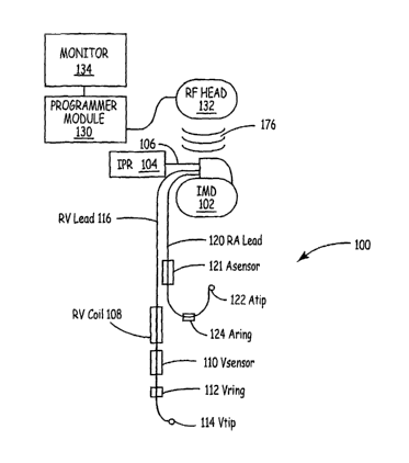
FIG. 1 is a schematic diagram of an implantable medical device system
according
to an embodiment of the invention;
FIG. 2 is a block diagram of an implantable medical device connected to a pair
of
sensor capsules;
CA 02500229 2005-03-24
WO 2004/028627 PCT/US2003/029936
3
FIG. 3 is a block diagram of an implantable medical device system implementing
a
sensor communication protocol between a programmer module, an IlVID and a
sensor
capsule;
FIG. 4 is a cross section of a co-axial two-wixe bus lead;
FIG. 5 is a sectional view of a mufti-lumen lead;
FIG. 6 is an axial view of a two-wire co-radial lead;
FIG. 7 is a sectional view of an exemplary wire used in a two-wire co-radial
lead;
FIG. 8 is an electrical model illustrating electrical interference of sensor
leads;
FIG. 9 is a schematic block diagram of a sensor interface system for an
implantable
medical device and a sensor capsule for lead fault detection;
FIG. 10 is graph of one bit time for communication across a two-wire bus
wherein
the bit time is divided into six equal parts;
FIG. 11 is a graph illustrating one bit time communication between a fast
sender
and a slow receiver;
FIG. 12 is a graph illustrating one bit time communication between a slow
sender
and a fast receiver;
FIG. 13 is a graph illustrating voltage swings on a two-wire bus;
FIG. 14 is a graph illustrating a start bit definition;
FIG. 15 is a graph illustrating a master driving a data "0";
FIG. 16 is a graph illustrating a master driving a data "1";
FIG. 17 is a graph illustrating a slave driving a data "0";
FIG. 18 is a graph illustrating a slave driving a data "1";
FIG. 19 is a graph illustrating a master stop, a master acknowledge request
("ack
req"), and a slave acknowledge ("slave ack");
FIG. 20 is a graph illustrating a master stop, a master ack req, and a slave
non-
acknowledge ("nack");
FIG. 21 is a graph illustrating a slave stop-stop-stop;
FIG. 22 is graph illustrating the sending of a message from the master to one
or
more slaves;
FIG. 23 is graph illustrating a response with data from a slave to the master;
FIG. 24 is a general command format for transfernng data across a two-wire
bus;
FIG. 25 is a table providing a slave long address format;
CA 02500229 2005-03-24
WO 2004/028627 PCT/US2003/029936
4
FIG. 26 is a table of slave short addresses arid multicast examples;
FIG. 27 is a graph of a triggering example;
FIG. 28 is a graph and table illustrating a relationship between triggering of
one
sensor and reading corresponding data;
FIG. 29 is a graph illustrating re-triggering of data using a count code;
FIG. 30 is a graph illustrating a collection of data points for an RV pressure
waveform;
FIG. 31 is a table illustrating Command Codes and measured parameters;
FIG. 32 is a table providing a command overview of a sensor interface for an
implantable medical device;
FIG. 33 is a table illustrating a Master's Unlocks command;
FIG. 34 is a table illustrating Unlock key options;
FIG. 35 is a table illustrating a Master's Search Long Address command;
FIG. 36 is table summarizing an example search across a sensor for an
implantable
medical device;
FIG. 37 is a table illustrating a Master's Write Short Address command;
FIG. 38 is a table illustrating a Trigger command;
FIG. 39 is a table illustrating a Trigger Command Code for a cardiac IMD;
FIG. 40 is a table illustrating an example of a Trigger Command Code for
Sonomicrometry transmitters and receivers;
FIG. 41 is a table illustrating a Quick Trigger command;
FIG. 42 is a table illustrating a Master's Read command;
FIG. 43 is a table illustrating a Slave's Read Response;
FIG. 44 is a table providing rules for a Read Results command;
FIG. 45 is a pair of tables illustrating an example of reading results from a
reading
buffer with 8 bit data and a count and a command code embedded;
FIG. 46 is a table illustrating a Master's Read Results command;
FIG. 47 is a table illustrating a Slave's Read Results example response;
FIG. 48 is a table illustrating a Master's Write command;
FIG. 49 is a table illustrating a Master's LSB FAM/REG Address command;
FIG. 50 is a table illustrating a Master's MSB RAM/REG Address command;
FIG. 51 is a table illustrating an LSB EEPROM Address command;
CA 02500229 2005-03-24
WO 2004/028627 PCT/US2003/029936
FIG. 52 is a table illustrating a MSB EEPROM Address command;
FIG. 53 is a table illustrating a Master's Copy RAM/REG to EEPROM memory
command;
FIG. 54 is a table illustrating a Master's Copy of EEPROM to RAM/REG memory
5 command;
FIG. 55 is a table illustrating a Master's Quick Read command;
FIG. 56 is a table illustrating a Master's Which Pointer to Read command; and
FIG. 57 is a Slave's Quick Read Response command.
With reference now to the drawings, wherein like numbers refer to like
elements
throughout, embodiments of the invention are now described. FIG. 1 is a
schematic
diagram of an implantable medical device system 100 according to an embodiment
of the
invention. As illustrated, implantable medical device ("IMD") 102 takes the
form of an
internal cardio defibrillator or pacemaker, for example, with implantable
pressure
reference, right ventricular ("RV") pressure, and RV oxygen. System 100
includes IMD
102 that communicates with internal pressure reference ("IPR") 104 by way of
communication bus 106.
IMD 102 is electrically connected with right ventricular coil ("RV coil") 108,
Vsensor 110, Vring 112, and Vtip 114 by way of right ventricular lead ("RV
lead") 116.
The RV lead 116 has a true bipolar lead (Vtip 114, Vring 112) for differential
sensing,
along with a Vsensor capsule 110, and RV Coil 108 for high voltage
defibrillation therapy.
The Vsensor capsule 110 contains a pressure sensor, an oxygen sensor, and a
temperature
sensor. The right atrial lead ("RA Lead") 120 is connected to Asensor 121, and
a true
bipolar lead (Atip 122, Aring 124).
In practice, a DC bias voltage of 3.0 V is maintained across RV Lead 116. Data
in
the form of 200 mV fluctuations are communicated on top of the 3.0 V bias. The
communication across the two-wire bus of system 100 seeks to minimize
resistance,
minimize capacitance, minimize inductance, maximize shielding and maximize
reliability.
The shielding is most easily maximized in a coaxial implementation with a
grounded outer
conductor and data/clock/power on the inner conductor.
IPR 104 has a separate lead whose communication bus 106 is hooked in parallel
with the other communication busses in RV Lead 116 and RA Lead 120. These all
share a
CA 02500229 2005-03-24
WO 2004/028627 PCT/US2003/029936
6
common pair of feedthrus into IMD 102. Pressure sensors are absolute pressure
sensors
that require temperature measurement capability. Accordingly, pressure changes
in a
capsule due to temperature effects are calibrated out. The sensors are
optionally
electrically connected in parallel with IMD 102 through a number of different
ways. In
this embodiment, each lead is plugged into a corresponding port in a connector
block and
electrical connections between the sensors are made inside the connector.
Programmer module 130 connnunicates with IMD 102 by way of RF Link 176
from RF Head 132. The programmer module 130 programs parameters, read status,
read
diagnostic data and stored waveforms, as well as real-time waveform data. IMD
102
collects data from IPR 104, an oxygen sensor, and temperature sensors at
regular intervals
on the ordex of every couple of seconds. Data is further collected from
Vsensor 110 at
rates up to 2048 samples per second. Information received from IMD 102 is
displayed on
programmer module 130 by way of monitor 134.
FIG. 2 is a block diagram of an implantable medical device system 140
including
1 S IMD 102 connected to sensor capsules 142 and 144 by way of two-wire bus
178. The
diagram schematically illustrates parallel electrical connection of sensor
capsules 142 and
144 to IMD 102 with each capsule containing more than one sensor.
IMD I02 includes micro-controller unit 146, which has a microcontroller memory
(RAM, ROM, EEPROM), telemetry port, and therapy circuitry (for pacing,
sensing,
defibrillation, and timing). Thexapy and diagnostic unit 148 provides an
accelerometer and
minute ventilation, diagnostic circuitry (electro-gram, wavefonm compression,
battery
monitoring, and lead monitoring), and basic infrastructure circuitry (power
supply
generation, ADC, and references, etc.). Clock 149 is provided within therapy
and
diagnostic unit 148 to provide timing to IMD 102 and the sensor capsules.
Power supply
147 is also provided within therapy and diagnostic unit 148 to provide power
to IMD I02
as well as external sensor capsules 142 and 144.
Communication unit 150 communicates with remote sensors and sends power as
well as a synchronizing signal or clock signal to remote sensors.
Communication unit 150
also contains a transceiver to transmit and receive data over a two-wire
communication
bus. Communication unit 150 has protection networks to protect IMD I02 against
transient voltages and currents induced on two-wire bus 178 due to electro-
surgery,
CA 02500229 2005-03-24
WO 2004/028627 PCT/US2003/029936
7
electrical discharge, defibrillation, electro-static discharge, electro-
magnetic interference,
etc.
Each sensor capsule 142 and 144 contains circuitry to measure and convert
pressure, temperature, and oxygen signals into a digital signal through analog
to digital
converters ("ADCs") 152. Each sensor capsule (142, 144) also contains a small
non-
volatile memory, in the form of EEPROM 154, to store a unique sensor address,
serial
number, and calibration coefficients, etc. Recovery units 156 recover power
from the
fluctuating voltages on two-wire bus 178 to power each respective sensor.
Clock synchronization allows a relatively inaccurate high speed clock recovery
unit 157 to be available on each sensor, which is periodically synchronized
with clock 149
on IMD I02. IMD 102 thereby controls the sampling rate and sampling time for
each of
the individual sensors by way of transmitting commands to the sensor(s),
thereby
instructing the sensors) to sample. IMD 102 also controls when each sensor
puts each bit
of data on the bus. The need for high accuracy clock generation circuits
within each sensor
capsule is therefore eliminated. A protection network is also included in each
sensor
capsule to minimize the effect of transient voltages and currents induced on
the two-wire
bus 178 due to electro-surgery, implantable caxdio defibrillator ("ICD")
discharge,
defibrillation, electro-static discharge, and electro-magnetic interference,
etc. As
particularly illustrated, sensor capsule 142 includes temp sensor 158 and
pressure sensor
160. Likewise, sensor capsule 144 includes temp sensor I62, pressure sensor
164, and
oxygen sensor 166.
FIG. 3 is a block diagram of implantable medical device system 170
implementing
sensor communication between programmer module 130, IMD 102 and sensor capsule
174. Three communication protocols are defined to move data from sensor
capsule 174 to
micro-controller 146 within IMD 102. The first protocol defines how sensor
data is
digitized and moved to a small buffer memory within recovery unit 156 in
sensor capsule
174. This protocol also defines how data is read/written from/to an EEPROM
within
sensor capsule 174 and placed into buffer memory. This protocol is defined by
hardware
within each sensor capsule.
The second protocol is a sensor communication protocol that defines how data
is
moved from memory within a transceiver at one end of two-wire bus 178 to
memory
within a transceiver at the other end of two-wixe bus 178. The sensor
communication
CA 02500229 2005-03-24
WO 2004/028627 PCT/US2003/029936
protocol defines an addressing scheme, data encoding, and voltage/current
levels on two-
wire bus 178. Finally, a third protocol defines how data is moved from a
transceiver
within IMD I02 to the appropriate locations. Once data is received by IMD 102,
it
becomes available in memory for signal processing, waveform compression,
telemetry,
and episode storage. This protocol is defined by hardware and firmware within
IMD 102.
The sensor communication protocol defines how data is moved between remote
sensors and IMD I02 via two-wire bus 178. Network protocols generally have
multiple
layers. The sensor communication protocol is therefore described using the
open system
interconnection ("OSI") model for a network. All layers defined in the OSI
model are not
necessary for the present invention. The OSI model is broken into 7 layers.
The physical
layer determines how a bit is moved across the wires (voltage, current,
timing). The data
link layer determines how frames of data axe created (bytes, words). The
network layer
determines how packets of data are assembled. The transport layer determines
how
packets are moved. The session layer defines how a session is started and
ended. The
presentation layer determines how data is compressed or encrypted. The
application layer
determines how data is used at the highest level. The application layer is
defined by the
cixcuits, firmware, RAMware, and software running in IMD 102 and/or programmer
module 130.
According to an embodiment of the present invention, the physical layer
determines how "1's" and "0's" are moved between IMD 102 and sensor capsules
174 via
two-wire bus 178. The physical layer also determines how remote sensors are
powered
from IMD I02. The two-wire bus 178 provides synchronization between sensors
174 and
IMD 102. This allows IMD 102 to control when a sensor makes a sample and
maintains
synchronous operation of all sensors. The physical layer also defines how the
integrity of
the wires can be checked.
The transmission of power from IMD 102 to remote sensor capsules is necessary
because the sensors are small enough to pass through the veins and into the
heart. The
size requirements for the sensors do not allow for a battery within the sensor
capsule itself.
Synchronization is important for applications requiring sensors at different
locations (e.g. EGM, RA and RV pressure). If each sensor sends data at a
slightly
different rate, it becomes more difficult for IMD 102 to create records of the
sensor data
because each sample is taken at a different points in time. Processing of the
data also
CA 02500229 2005-03-24
WO 2004/028627 PCT/US2003/029936
9
becomes difficult because the time base for the samples is slightly different.
For example,
calculating a simple difference between RA and RV pressure is complicated if
the sample
rates are not the same. Data would then be collected at a higher rate from one
of the
sensors and interpolation or other filtering techniques would be required to
time align the
sample data. The synchronization signal also allows the clock circuitry within
each sensor
to be less accurate. If each sensor has to provide data at the same rate
without a
synchronizing signal, crystal controlled oscillators would be required, which
would add
significantly to the size of the sensor capsule.
Integrity of two-wire bus 178 is continually verified during operation.
Numerous
faults could occur on the wires, which could have important implications for
therapy
supplied by IMD 102. If the outer insulation of the wires fails in a way that
allows currant
to flow through the heart muscle, the heart could be stimulated or
fibrillation could be
induced. If an insulation fault occurs between the two wires of two-wire bus
178, the
battery of IMD 102 could be drained or loaded, thereby causing a loss of
longevity or loss
of function in IMD 102. If a wire break occurs, a loss in communication with
the sensor
would likely occur.
EMI filters and/or high voltage protection networks may be optionally
installed on
IMD 102 and possibly in sensor capsule 174. These networks add capacitance and
series
impedance, which tend to increase power supply current when driving two-wire
bus 178.
Furthermore, the use of these networks slows down transitions on the bus and
may limit
bandwidth.
The wires used to connect the sensors to IMD 102 have characteristics that
limit
the performance of the bus in terms of data rate, current drain, and noise
immunity. The
wire characteristics also affect how signals on the bus couple to adjacent
wires on the lead
and interfere with these signals. The physical construction of the wires
further defines the
types of faults in the wires that are most likely to occur and impacts how
fault detecting
circuitry should operate.
FIG. 4 is a cross section of a typical two-wire bus lead in the form of co-
axial lead
180. Outer coil 182 is connected to the sensor capsule, and to system ground
on IMD 102.
Inner coil 184 is also connected between a sensor capsule and IMD 102, and is
used for
communication. A stylet is insertable within inner coil 184 to aid in
positioning the sensor
at the time of input.
CA 02500229 2005-03-24
WO 2004/028627 PCT/US2003/029936
Bus insulation layer I 86 surrounds and protects inner coil 184 and outer coil
182.
The outer coil is covered by outer coil insulation layer 183 while inner coil
184 is covered
by inner coil insulation layer 188. A gap 185 is formed between inner coil
insulation layer
188 and outer coil insulation layer 183. Gap 185 may be air if lead 180 is dry
or may
gradually fill with water if lead 180 is wet.
Bus insulation layer 186 and inner coil insulation layer 188 are preferably
made
from polyurethane (Pellathane 80A). Layers 186 and 188 may optionally be made
from a
biocompatible insulating material including polyurethanes, ETFE, silicone, or
polyamides.
Insulating materials with low dielectric coefficients are preferred to
minimize capacitance
10 between conductors. The gaps between the insulation and conductors will be
air when the
lead is dry or may gradually fill with water when the lead is wet. Outer coil
182 and inner
coil I84 can be made from biocompatible conductive materials including MP35N,
platinum, or silver cored MP35N. Conductive materials with low resistance are
preferred.
FIG. 5 is a sectional view of rnulti-lumen lead 190. In particular, mufti-
lumen lead
190 is a three lumen high voltage lead intended fox an implantable
cardiodefibrillator
("ICD") and pressure sensing application. Lead 190 supports integrated bipolar
sensing, a
high voltage RV coil, and uses a coaxial cable for communication with a
pressure sensor.
Lead 190 includes a plurality of compression lumens 192 defined by lead body
194. Each
lumen has an OD = 0.029" while lead body 194 is preferably made from silicone.
Lead
190 uses one cable with a coil 196, one coil 198, and a cable for HV coil 200.
The
diameter of lead 190 is defined by D = 0.105".
The coil 198 is connected to the tip electrode and is used to allow the stylet
to pass
through to the tip. The cable within coil 196 is used for sensor communication
and is
preferably silver cored MP35N with an ETFE insulating layer. Cable 200 is used
for a
high voltage ("HV") coil. The resistance of the conductors is low (« 5 ohms)
due to the
use of silver core/MP35N wire.
FIG. 6 is an axial view of two-wire co-radial lead 2I0 that uses a co-radial,
mufti-conductor construction. Lead 210 uses four individual wires wound side
by side.
Two wires are connected to signal "a" and two wires are connected to signal
"b." The
inner diameter of lead 210 is about 20 mils, with the outer diameter of wires
being about
37 mils. An outer insulation of polyurethane is used to provide further
protection. The
inner diameter of polyurethane insulation is 45 mils with the outer diameter
of
CA 02500229 2005-03-24
WO 2004/028627 PCT/US2003/029936
11
polyurethane insulation 216 being 57 mils. Wires 212(a), 213(a), 214(b) and
215(b) are
wound adjacent to each other rather than one on the outside and one on the
inside. The
wires are wound together with two wires used for each signal. Polyurethane
tubing 216
covers each of wires 212 - 215.
FIG. 7 is a sectional view of the conductors used within the co-radial lead
210,
including a 3.5 mil diameter coxe 218 preferably of silver cored MP35N. Wire
core 218 is
dipped in a polyamide coating 220 to achieve a thickness of about 0.5 mils.
Each wire 212
is further insulated with outer insulation 222 ETFE to a thickness of
approximately 2 mils
to obtain a total thickness for each insulated wire of about 8.5 mils. Four
wires are then
wound side by side to achieve a lead with an inner diametex ("ID") of
approximately 20
mils. A SSD polyurethane tubing 216 approximately 6 mils thick is then slipped
over the
lead conductors to provide a final layer of insulation.
FIG. 8 is an electrical model 230 illustrating electrical interference of
sensor leads.
Electrical model 230 includes IMD 102, which includes transceiver 234 and
stimulus
circuits 236. Inner wire 238 and outer wire 240 connect IMD 102 to sensor
capsule 242
and sensor capsule 244. Each sensor capsule has an interior transceiver 246.
Electrical
interference from stimulus circuits 236 to the body tissue are modeled through
ring 248,
tip 250 and case 252.
There are several variables that affect performance of the communication link,
such as signals on the wires coupling into the body causing sensing errors,
signals in the
body coupling into the wires causing data errors, EMI coupling into the wires
causing data
errors, CVF current, and effects due to sensors turning on/off. These factors
can change
by several orders of magnitude depending on the lead parameters, methods used
for
stimulating tissue and sensing, as well as methods used for EMI and high
voltage
protection in IMD 102.
In electrical model 230, Cio 260 models the capacitance from inner conductor
to
outer conductor of the coaxial cable. Cio 260 directly affects current drain
of the system
because current is proportional to capacitance * voltage * frequency ("CVF").
Cob 262
models the capacitance from outer conductor to the body tissue. Cob 262
directly affects
crosstalk from external noise sources into the communication lead and allows
communication signals to couple into the body, where they could cause sensing
problems
in IMD 102. Cib 264 models coupling from the inner conductor of the cable to
the body.
CA 02500229 2005-03-24
WO 2004/028627 PCT/US2003/029936
12
Normally this will be very low in a coaxial lead configuration because the
outer conductor
shields the inner conductor from the body. Ri 266 and Ro 268 model the
resistance
properties of the inner and outer conductors. Ro 268 is especially important
for xejecting
noise from the body and for preventing crosstalk from the communication
protocol to the
S body. Any voltage change in the body relative to ground results in a current
flow in the
outer conductor due to Cob 262. This current is converted to a voltage by the
resistance of
the outer conductor Ro 268.
The tip 250, ring 248, and case 2S2 of the stimulus/sensing electrodes are
modeled
as if coupled to the body through resistors. In reality, these electrodes are
complex
distributed impedances. IMD 102 is shown electrically connected to the lead
through the
body tissue. Case 252 of IMD 102 is typically the largest electrode in a
pacemaker/ICD
and is typically the most representative of the voltage seen in the body. In
some IMDs, the
case is tied to system ground through a low impedance switch, while in others
the case is
left floating. In this example, Rtr 270 and Rtc 272 are modeled as 830 ohm
resistors,
while Rrc 274 is modeled as a 41 S ohm resistor.
During a bipolar pace sequence, case 252 is left floating, ring electrode 248
is tied
to system ground, and tip 2S0 is driven to a large negative voltage (0 to -9
V). The case
voltage ends up somewhere in between the tip and ring voltage, but typically
stays closer
to ring 248 than tip 2S0 because the ring electrode area is typically larger
than the tip,
thereby creating a lower impedance connection. For a unipolar pace, case 2S2
is held to
ground while tip 250 is driven negative. In this scenario, case 252 stays
close to ground.
In some pacing systems, the stimulus circuits ground the tip, while pulsing
the zing
or case positive. In these systems, the case typically moves a greater
distance from ground
thereby inducing a larger voltage in the body relative to system ground.
Depending on the
method of implementation for the pacing system, voltage pulses on the case may
reach 9
V with respect to system ground. In nerve stimulators, this value can be as
high as 1S V.
Rise times for the leading edges of pacing pulses are typically on the order
of 100 ns - 1
us.
Pacemakers and implantable cardiodefibrillators ("ICDs") typically address
high
voltage protection differently. In an ICD, the case moves as much as 800 V
with respect
to ground during discharge. Rise times on ICD pulses are typically very fast
with slew
rates on the order of S00 V/us at the leading edge. During trans thoracic
defibrillation, the
CA 02500229 2005-03-24
WO 2004/028627 PCT/US2003/029936
13
case moves as much as 1600 V with respect to ground. Rise times on trans
thoracic
defibrillation pulses are typically much slower than for ICD's.
In a pacemaker, voltage on the leads is clamped with protection networks. This
reduces the voltage on the leads as seen by the implantable medical device
("IMD"), but
the voltage is still very large in the body. Similar voltages can be seen in
the body during
electro-surgery. A voltage limiting network may be incorporated within IMD 102
and in
the sensors.
Interference into the communication wires can occur if the capacitance on the
outer
lead conductor is large and the impedance of the outer lead conductor is
large. As an
I O example, a large amplitude unipolar pace in a pacemaker uses a pace case
architecture
with the sensor lead outer conductor grounded. The voltage induced on the lead
outer
conductor during the pulse rise time is approximately:
Cob ~ Vpace~ ~a + Rsu~itch~
T~outer
tfall EQ. 1
In EQ. I, Cob is the capacitance between outer conductor and body, Vpace is
the
15 voltage on the body relative to ground, tfall is the fall time on the
leading edge of the pace,
Ro is the resistance in series with the outer conductor and is assumed to be
distributed, and
Rswitch is the value of the switch on IMD 102 used to connect the lead outer
conductor to
ground (about 10 Ohms). Thus, it can be seen that interference is minimized by
reducing
Cob, Ro, Rswitch and increasing tfall.
20 From the above example, the lead conductor capacitance arid resistance
properties
play an important part in rejecting interference from pacing pulses. The high-
voltage
multi-lumen lead construction has significantly better performance than the co-
axial lead
or the co-radial designs due to lower resistance and lower capacitance
properties. Further,
the architecture used for the pacing circuits and the rise time of the
stimulus pulses will be
25 important in reducing the amount of crosstalk. Finally, using the co-radial
construction
lead results in enough coupling from the pacing pulses to the sensor signal to
disrupt
communications, if the pulses occur when the signal line is not strongly
driven.
Just as voltages on the body can be coupled into the wires used for
communications, voltage on wires can be coupled into the body causing
interference with
30 sensing operation within IMD 102. Three scenarios are set forth below
wherein the
CA 02500229 2005-03-24
WO 2004/028627 PCT/US2003/029936
14
coupling to the body could be a factor: from lead inner conductor (through
Cib), from the
lead outer conductor (through Cob) due to the DC current needed to power the
sensor, and
from lead outer conductor due to transient current flowing in the leads during
voltage
transitions from communications.
First, coupling from the lead conductor directly to the body is addressed. Any
capacitance between the clock/power/data line to the body may cause an
attenuated
version of the voltage (Vsignal) on the communication lines to be coupled into
the body as
a common mode signal to tip 250, ring 248, and case 252. A capacitive divider
effect will
be formed by Cib, Cob, and Cbody to ground.
llbody ~ Cib ~ Trsigrral
Cib + Cob + Cbody gQ, 2
This coupling is minimized by reducing Cib and minimizing the voltage
transistors
on the lead used for communications.
Next is considered a situation where a sensor is enabled and the current
flowing
through the lead outer conductor causes a voltage drop across the conductor,
which is then
capacitively coupled into the body through the lead outer insulation. The
voltage induced
on the lead outer conductor is dependent on the sensor current (Isensor) and
the impedance
in the lead outer conductor (Rswitch + Ro). The voltage is then coupled into
the body
through Cob.
T~outer ~ Isensor ~ (Ro+ Rswitch) gQ, 3
This coupling is minimized by reducing Cob, Ro, Rswitch, and Tsensor.
Alternatively, a resistive impedance could be added to the tip, ring, or case
to allow the
common mode voltage to quickly bleed away.
Last considered is a coupling from the lead outer conductor. In this case, tip
250,
ring 248, and case 252 of IMD 102 float relative to circuit ground. Very fast
rise time 200
mV communication pulses with 100 Ohm source impedance are applied to the lead
inner
conductor with the lead outer conductor grounded. The resistance of the lead
outer
conductor plus any switch resistances cause the current through the lead outer
conductor to
result in a voltage drop. This results in a voltage spike that will quickly
bleed away. .The
peak of the spike is given by:
CA 02500229 2005-03-24
WO 2004/028627 PCT/US2003/029936
Ro + twitch
Pouter ~ 2 Ri Ro ~ YsigYCal
Rsource + ~ + 2 + Rswitch
EQ. 4
The magnitude of Vouter is reduced by minimizing Ro, Rswitch and Vsignal, and
maximizing Rsource.
The time constant of the decay is given by:
Tau ~ ( 20 + Rswitch+ Rsource+ Rswitch) ~ Cio
EQ. 5
Tau can be minimized by reducing Ro, Rswitch, and Cio.
This voltage is coupled through the capacitance of the lead outer conductor
into the
body causing a common mode step in voltage on the tip, ring, and case. These
glitches
10 appear as common mode spikes on tip, ring, and case electrodes, which are
then be filtered
by circuits in the IlVID. Typically, sense amplifiers have good common mode
rejection
and high frequency filtering of the input signals. As an example, if a sense
amplifier or
EGM amplifier had a first order low pass filter at 150 Hz, this results in an
attenuation of
the glitch amplitude of approximately 10,000X. For coupling through the lead
outer
15 conductor, the multi-lumen approach provides the least coupling and the
fastest decay time
making any filtering more effective as well as reducing the peak amplitude.
The lead properties have an effect on cross-talk from communications taking
place
on the sensor wires to the signals on the lead. Also, the effect of turning
high current
sensors on and off can induce voltages in the body large enough to disrupt
sense amplifiers
or impedance measuring circuits. The cross talk performance of the high
voltage
mufti-lumen lead is better than the co-axial lead or the co-radial
construction lead.
Crosstalk can be reduced by minimizing the amplitude of the voltages used on
the bus and
by reducing the rise/fall times of the signals. The addition of capacitance or
resistance to
the tip, ring, or case to ground can also help significantly.
There are several potential wire faults that can affect safety and reliability
of the
system. Typical causes of damage to Ieads include: cxushing of the lead,
environmental
stress cracking, scalpel nicks, and work hardening of the metal or insulation
due to many
cycles of flexing. These Iead failures can cause gaps in the insulation layers
resulting in
impedance paths between adjacent conductors and/or impedance paths between the
CA 02500229 2005-03-24
WO 2004/028627 PCT/US2003/029936
16
conductors and the body. The lead failures can also cause high impedance paths
in the
wires.
Safety issues include prevention of DC current flow into the body tissue and
prevention of inadvertent stimulation of tissue for a scenario where the
insulation fails.
Another issue is that a lead fault does not cause a high current condition
that could cause
the battery within the IMD to discharge prematurely. In the presence of a lead
fault, the
system should not allow a DC leakage path to the body with an average current
greater
than 100 nA over 1 second or a pulsed current condition in excess of 100 uA
for 0.5 ms.
Options for implementing a leakage detection circuit include issuing a command
to
the sensors to completely power down the sensors on the bus to allow a leakage
check
between the conductors and the body at normal supply voltages. Another option
is to drop
the voltage on the bus to a low voltage level (350 - 400 mV), which can result
in a "0"
current state for the sensors on the bus. A preferred mode of implementation
is to issue a
broadcast command to all bus sensors to go to a "0" current state for a period
of time long
enough to check for leakage. Circuitry in the IMD may then check for faults
between each
of the conductors or between each of the conductors and the body.
An important possible lead fault concerns failure of the outer insulation. To
minimize the impact of this possible fault, the outer conductor should be
maintained at the
same DC potential as the body. Some IMDs use a positive battery terminal as a
body
ground while others use a negative terminal as body ground. In this case, the
outer
conductor of the lead could be driven to either the positive supply voltage or
negative
supply voltage. However, a rectifier function within each sensor would be
required to
allow the conductor polarity to be different for different IMDs. If the co-
radial
construction method is used, and there is a lead outer insulation fault, there
is no shield
layer to prevent current flow to the body. Thus, the possibility of a lead
insulation fault
that could cause a DC current flow into the body is greater.
FIG. 9 is a schematic block diagram of a sensor interface system 280 for an
implantable medical device ("IMD") 102 and a sensor capsule 284 for lead fault
detection.
IMD 102 is capable of switching the transceiver and sensor power source 286 or
a leakage
detection circuit 288 onto inner conductor 290 or outer conductor 292. The
outer
conductor 292 of the lead is normally connected to body ground, but can be
isolated by a
switch. The sensor capsule 284 includes a rectifier & regulator 294 to accept
voltages of
CA 02500229 2005-03-24
WO 2004/028627 PCT/US2003/029936
I~
arbitrary polarity from IMD I02. The sensor capsule 284 includes sensor 298
and also
includes isolation circuits 296 for isolating the rectifier and regulator 294
and transceiver
295 from the lead conductors, during a lead integrity check.
Currently developed sensors have differing operating voltage requirements.
With
multiple sensors on a bus, it is desirable to provide as large a DC voltage as
is practical for
the supply, and allow each sensor to regulate the required voltage to a
required level. This
also reduces the effects of line voltage drops due to changing load currents.
The
maximum voltage level conveniently available in IMD 102 is the unregulated
battery
voltage, which can be as high as 3.3 V at beginning of life, typically 2.65 V
at an elective
replacement indicator, and as low as 1.8 to 2.2 V at end of battery life.
Each sensor has a different operating current drain. Most have low operating
currents (I - 10 uA) and will be turned on for a few milliseconds each second
or run
continuously. Some sensors, and/or the EEPROMs within the sensors, may require
currents in the milliamp range. If the source impedance of the battery, supply
circuitry,
I 5 and wire resistance is high, the milliamp current pulses could disrupt
communications. A
few methods are available to address this issue, such as formulating a design
protocol to
operate through the high current pulses or suspending communications during
high current
measurement. Another method includes storing charge on a capacitor in the high
current
sensor and to isolate the sensor from the bus. The preferable method is to
suspend
communications during high current measurement.
A two-wire bus provides power, clock, and data from a single master to up to
16
slave devices. Half duplex communications, and pulse width modulation of the
voltage on
the bus allow a raw data rate of approximately 100 Kbps. The "1's" and "0's"
are encoded
the same for master and slave devices. An initialization procedure is used to
determine the
long address of each slave device and to assign a short address to keep the
commands
shorter. The protocol includes messages to trigger measurements, write, and
read data.
Addressing modes are provided to allow individual devices, groups of devices,
or all
devices to be addressed. The message format includes start, command word,
address,
data, CRC, and stop. Some messages require acknowledge by the recipient while
others
do not. The master device always initiates communications. It is not allowable
for a slave
device to put data on the bus without the master first requesting the data.
CA 02500229 2005-03-24
WO 2004/028627 PCT/US2003/029936
18
The start of a message is indicated by pulling the bus low for 2 bit times
nominally.
This serves to wake up all slaves such that they are ready to read messages.
FIG. 10 is graph of nominally one bit time for communication across a two-wire
bus wherein the bit time is divided into 6 equal parts. One bit time can allow
up to an 8%
tolerance on the clock in both the sender and receiver.
FIG. 11 is a graph illustrating one bit time communication between a fast
sender
and a slow receiver. In this case, one bit time ends up being 10 us - (0.08 x
10 us) = 9.2
us.
FIG. 12 is a graph illustrating one bit time communication between a slow
sender
and a fast receiver. In this case, one bit time ends up being 10 us + (0.08 x
10 us) = 10.8
us.
FIG. 13 is a graph illustrating voltage swings on a two-wire bus. The voltage
swings are 200 mV. Signals are driven on the two-wire bus. One wire is labeled
"MW DATA" and is driven between Bplus and Bplus - 200 mV. The other wire is
labeled "MW SHEILD."
FIG. 14 is a graph illustrating a start bit definition. The start of a message
is
nominally a bus low for two bit times, however some variation on clock
mismatch is
allowed between slave and master so that the slave can wake up and detect the
start bit.
The sending of a message from the master to a slave device is first described.
The
start of a data bit in the message begins with the master pulling the bus up
to a high
voltage. A fraction of a bit time later, the master pulls the bus back low.
The duration of
the high voltage pulse indicates the data value.
FIG. 15 is a graph illustrating a master driving a data "0". A data value with
a time
high of 1/3 bit time corresponds to a logic "0".
FIG. 16 is a graph illustrating a master driving a data "1". A data value with
a time
high of 2/3 bit time corresponds to a logic "1". In its simplest form, the
slave's receiver
samples the data on the bus with a time delay of 1/2 bit time (t3) after the
rising edge of
the bus.
FIG. 17 is a graph illustrating a slave driving a data "0", and FIG. 18 is a
graph
illustrating a slave driving a data "1". The master is the only one on the bus
with pull-up
capability. At the end of the bit time, the master again pulls the bus high
starting a new bit
time. When the slave drives data onto the bus, the slave can only pull the bus
down.
CA 02500229 2005-03-24
WO 2004/028627 PCT/US2003/029936
19
Because the slave cannot pull up, the slave uses timing information to
determine whether
to send a data "1" or "0". This is essentially the same as when the master is
sending "1's"
and "0's" but the slave shares driving of the bus with the master.
FIG. 19 is a graph illustrating a master stop, a master acknowledge request
("ack
req"), and a slave acknowledge ("slave ack"). A stop bit is indicated by the
bus being held
high continuously for 1 bit time. The master can send out commands to multiple
slaves.
If multiple slaves are responding, then some slaves may be acknowledging the
message
and others may not. A rnulti-slave acknowledge therefore is of limited value
because if
received, the master only knows that at least one slave received the message.
The master
ends commands with a sequence that the data link layer refers to as Stop-Ack
Req-(I~Ack. If the master requires an ACK to the last command, the master will
put a
logic "0" on the bus in the bit time immediately following the stop bit. If a
request for an
ACK is given, the slave device will respond with a logic "1" in the next bit
time as an
indication that the slave received the message.
FIG. 20 is a graph illustrating a master stop, a master ack req, and a slave
non-
acknowledge ("nack"). If the slave does not receive the message at all, or if
the message is
received with an error, no ACK or NACK will be provided and the command will
be
ignored. Defining what is an error based on the command structure and error
checking is
also further defined in the data link layer.
FIG. 21 is a graph illustrating a slave stop-stop-stop. When the slave drives
data
onto the bus in response to a command, the slave drives "1's" and "0's" out to
the master.
Upon the last bit of data being sent, the master is still unsure if any more
data is to follow.
Accordingly, the master allows three chances for the slave to send more data.
This is
referred to as a STOP-STOP-STOP. The stop bit from the slave is indicated by
the lack of
data on the bus for a period of 1 bit time for a consecutive 3 bit times in a
row. The stop
sequence occurs for 3 bit times in a row to avoid conflict on the bus where
the sensor is
pulling down and the master is pulling up at the same time.
FIG. 22 is graph illustrating the sending of a message from the master to one
or
more slaves. Thus, a message from the master to one or more slaves is
summarized as a
start sequence, some data, and a stop sequence.
The slave device uses a delay chain triggered off the rising edge of the bus
to
determine when to sample the bus voltage. The rising edge of the bus is used
to reset the
CA 02500229 2005-03-24
WO 2004/028627 PCT/US2003/029936
falling edge of the slave's clock low and the 1/2 bit time delay after the
rising edge of the
bus is used to set the slave's clock high. The clock is then used to sample
the data on the
bus and to synchronize the data with the clock.
FIG. 23 is graph illustrating a response with data from a slave to master.
First, the
master requests data from the slave by sending a complete message. All
commands that
require data from the slave will be preceded by the ACK request. The slave
will then put
an ACK on the bus and follow up with data. The master then pulls the bus high
for 1/6 of
a bit time and releases the bus. The slave puts data on the bus in the same
manner as the
master did when the master was sending data by pulling the bus low. The
duration of the
10 high voltage pulse indicates the data value with a time high of 1/3 bit
time corresponding
to a logic "0" and a time of 2/3 bit time corresponding to a logic "1". Once
the slave has
pulled the bus low, the slave releases the bus at t = 5/6 of a bit time. The
master continues
to pull the bus high at the start of each bit time until the master receives a
stop bit by the
slave indicating the data transmission is complete. When the master recognizes
the stop
15 bit from the slave and determines that the message was received correctly,
the master
finishes the stop command by putting two more stop bits on the bus.
To prevent contention on the bus, the bus master releases the bus before the
sensor
tries to pull it low. The slave also releases the bus before the master pulls
the bus back
high. To meet this requirement, the longest value possible for 5/6 of a bit
time seen in the
20 sensor must be less than the shortest value possible for 1 bit time as seen
by the master.
This puts an accuracy tolerance on the time delays of about +/- 8% if rise-
fall times and
propagation delays for detecting clocks and turning on/off pull-ups and pull
downs are
neglected.
The task of a data link layer is to take a raw transmission facility and
transform it
into a line that appears free of transmission errors. The data link layer
accomplishes this
task by breaking up the input data into data frames, transmitting the frames
sequentially,
and then processing the acknowledgment frames sent back by the receiver. The
application layer determines the set of allowed messages and the action taken
upon receipt
of each.
Data transmission is based on a master - slave relationship. The master
initiates all
communication by sending commands to the slave, which then responds with
actions or
data. This allows more hardware intelligence to be placed in the master IMD,
which has
CA 02500229 2005-03-24
WO 2004/028627 PCT/US2003/029936
21
more resources such as a battery, a crystal oscillator controlled time base,
and more area
for integrated circuits and external components. The slave electronics are
provided to be
simple and low in power. The slave may, of course, still support intelligent
operations.
Signal processing in the slave allows the sending of processed data rather
than raw data
back to the master, thereby resulting in fewer transferred data bits.
FIG. 24 is a general command format for transferring data across a two-wire
bus.
Commands are preceded by a Start sequence and all slaves on the bus wake up in
response
to a Start. The fields are labeled Masterl through Master7, implying that the
master is
talking. The data is sent out from the most significant bit ("msb") first
proceeding to the
least significant bit ("lsb").
The field formats are configured as follows. The Start field is a unique 2 bit
time
long sequence issued by the master. The Slaves) field is a field to identify
one slave
(unicast) multiple slaves (multicast) or all slaves (broadcast). The Slaves)
field is
explained more fully below with regard to addressing. The Quick Trigger ("QT")
field is a
special field identifying a Quick Trigger ("QT bit set") command. All commands
except
the Quick Trigger ("QT bit set") have this bit set to zero. When the QT bit is
set high, the
command is identified as a Quick Trigger command.
The Master Command Name field provides instruction to the slave. A 5 bit
command in the Master Command Name field identifies up to 32 different
commands. If
the QT bit is set, then this field is not used. The Data field is 8 bits long
for most
commands. The use of 8 bits allows a byte of data to be written at a time. The
data field
varies from command to command and can be broken down to sub-fields. The frame
check sequence ("FCS") field provides error checking. The FCS field is used
for a cyclic
redundancy check ("CRC").
The Stop Sequence field is used to tell the slave when the master is talking
and that
this is the end of the command. When the slave is talking, the stop sequence
is used to tell
the master that this is the end of the data. The stop sequences takes two
forms, namely
Stop-Ack Req-(N)Ack and ftop-Stop-Stop. In the Stop-Ack Req-(I~Ack form, the
talker
is asking the listener if they received the message and if the message was
error free. "Ack
Req" means Acknowledge Request, "Ack" means Acknowledge, and "(N)Ack" means
Not
Acknowledge. The Stop-Stop-Stop form is slave data response for the Read and
Read
Results conunands. A bit time is a unit of time (clock cycle) for a "1" or
"0".
CA 02500229 2005-03-24
WO 2004/028627 PCT/US2003/029936
22
The command format length is 33 bit times for most commands. Because most
commands are the same length and format, a simpler form of digital electronics
is allowed
in a capsule (hermetic body) on a lead. Of course, this area is extremely
constrained.
The sensor interface allows the slaves to sleep, thereby saving power. The bus
can
have multiple slaves hanging on it. These slaves may be sensors, actuators or
slave IMDs.
The command structure is implemented with the Master initiating all
communication.
When the Master starts talking, the Master issues a Start command. All slaves
begin
listening on a Start command.
A slave not being addressed by the master may stop listening and interpreting
the
command to save power. When a particular slave determines that a command is
not
directed to that slave, the slave may go to sleep until the next Start
sequence. Sleep mode
may occur at different points in the command format, depending on whether the
sensor is
mapped or unmapped. A mapped sensor has an assigned short address and unmapped
sensor does not have a short address.
Addressing is provided in two forms: long address, and short address. The long
address is 64 bits while the short address in the command is 6 bits. The long
address
uniquely identifies the slave telling: 1. manufacturer; 2, protocol version;
3. model
identifier; 4. unique serial number; 5. manufacturing facility; and 6. slave
number (useful
for identifying multiple slaves on a single lead). Error checking of the Long
Address is
performed internally within the sensor via CRC check or other standard
checking
procedure.
FIG. 25 is a table providing a slave long address format. 'The long address
contains
many bits and the current drain of the data communication is governed by i =
cvf, where c
= capacitance of the bus, v = voltage swing of data communicating on the bus,
and f =
frequency of the data on the bus. If the 64 bit long address is used for all
commands, the
frequency of data on the bus would be exceedingly large for an implantable
system. The
goal is to have a command structure that allows a map assignment of long
addresses to
short addresses such that the majority of communication is provided by short
addresses.
The use of a short address containing only 6 bits will lower the cvf current
of the bus. The
master communicates to the slaves three different ways: 1. Unicast to one
sensor; 2
Multicast (Trigger) up to four slaves simultaneously; and 3. Broadcast to all
slaves. A
CA 02500229 2005-03-24
WO 2004/028627 PCT/US2003/029936
23
broadcast is sent to every sensor on the bus, and there can be up to 16 slaves
simultaneously on the bus.
The 6 bit address is provided to trigger, i.e. Multicast, multiple slaves
simultaneously. The 6 bit format permits identification of 16 sensors uniquely
and permits
all short addresses sent to the sensors to be of the same format. The 6 bit
format allows
some multicast capability and a unique broadcast code.
FIG. 26 is a table of slave short addresses and multicast examples. The table
particularly illustrates examples of how the master specifies the short
addresses.
According to a preferred embodiment, multicasting of more than four slaves is
not
permitted.
Addressing at power up is particularly considered as follows. Slaves are
powered
up or reset and respond only to their long address. In this state they are
unmapped, and
only three commands are usable in this state: 1. Unlocks; 2. Search Long
Address; and 3.
Write Short Address. These commands can all use a reserved short address with
a code of
3F1~. This reserved code is used as a broadcast command going to all slaves on
the bus.
When the master uses the broadcast short address of 3F16, then all slaves
listen. The
master may then uniquely identify a particular slave depending on whether the
command
calls for a long address.
After power up, the long addresses of the slaves are searched. The sequence is
as
follows: 1. Use the Unlocks command and ensure all slaves are unmapped -
forcing all the
slaves to be unmapped; 2. Use the Unlocks command and check for any slaves on
the bus
"check for unmapped" (if a slave on the bus then proceed to next step); 3. Use
the Search
Long Address and search for the long address of the slaves) (once all slave
long addresses
proceed to next step); and 4. Assign each slave a unique short address via the
conunand
Write Short Address.
The assignment of long addresses are made during manufacturing. Long addresses
may be assigned to various slaves on a pacing lead or to a slave IMD, one
slave at a time
before each slave is added to the bus. A capsule on a lead is a hermetic body
that contains
the slave's electronics.
If a capsule contains multiple slaves, the four bit slave number included in
the long
address can be uniquely hard coded. At capsule test, the master searches the
unique long
addresses and assign short addresses. The capsule containing multiple slaves
then only
CA 02500229 2005-03-24
WO 2004/028627 PCT/US2003/029936
24
requires one pair of wires for all slaves. For increased safety, the Unlocks
command has a
form that "unlocks" the ability to write long addresses. If a lead contains
multiple capsules
the capsules are assigned unique addresses before they are built into a lead.
Each capsule's
long address is therefore searched out using the Search Long Address command.
Data going to or from the master contains a Frame Check Sequence ("FCS"). The
FCS is an 8 bit CRC. The generator polynomial G(x) is given as follows:
G(x) = x8 + xs + x4 + 1 EQ, 6
Polynomial strings are based upon treating bit strings as representations of
polynomials with coefficients of "0 and "1". Therefore, for example, the
generator
polynomial is the bit string 10011 00012.
The master controls when slaves sample by issuing triggers. The issued
triggers
ensure that all samples are evenly spaced for a particular slave and ensure
that all slaves
are sampling at the same time or multiples of each other, i.e. data alignment
slave to slave.
Furthermore, the issued triggers allow the master to control the data rates.
The slave's
ADC will require a certain amount of time to perform a conversion.
The are two trigger commands: Trigger, and Quick Trigger. The Trigger
command allows two additional fields of 4 bits each. One field allows time
stamping of
data via a Count embedded in the trigger command. This allows the master to
tell if a
sensor missed a triggers) and which triggers) were missed. Another field will
allow
Command Codes to be sent down to the sensor. The sensor may perform signal
processing of the data stream between two different Command Codes. Command
Codes
work like a 4 bit write within the Trigger command.
FIG. 27 is a graph of a triggering example. As illustrated, the read that
follows a
trigger does not obtain data from the most recent trigger but rather obtains
data from 4
triggers previous.
FIG. 28 is a graph and table illustrating a relationship between triggering of
one
sensor and reading corresponding data. The graph particularly illustrates an
example of
triggering four slaves at a same trigger frequency and the staggering of
reading the data
back to distribute the bus traffic evenly. The Counts that were sent with the
triggers are
stored in with the data.
CA 02500229 2005-03-24
WO 2004/028627 PCT/US2003/029936
The Quick Trigger (QT bit set) works just like the Trigger command, but is
less
flexible and allows power savings. The Quick Trigger command does not have a
Master
Command Name and does not have a Command Code. The inclusion of the Quick
Trigger command adds a 1 bit overhead to all the other commands but saves 9
bits on the
most frequent operation of triggering.
FIG. 29 is a graph illustrating re-triggering of data using a count code. On
occasion, re-triggering of a sample may occur. Re-triggering is a Trigger or a
Quick
Trigger command with a count code of Ehex. Re-triggering may be used if the
slope of
10 the data is not important or is not adversely effected by a re-trigger. Re-
triggering may
also be used if the sample period is long compared to the time between the
trigger and the
re-trigger of a sample (implying the slope is not adversely effected).
Further, a re-trigger
may be used if the data is non-periodic or if only a single sensor is being
triggered.
When the trigger is broadcast to multiple sensors, the acknowledge request can
be
15 meaningless because more than one sensor is acknowledging proper receipt of
the trigger
command. When the trigger goes out to a single sensor, the acknowledge has
more
meaning because the acknowledge is specific to a single sensor. Therefore, if
the trigger is
NACK'd, the trigger can be determined if re-triggering can be performed. A re-
trigger
may get ACK'd thereby returning some semblance of periodic triggering.
20 Sorne forms of digital signal processing may be performed in the sensor.
The
signal processing for RV Pressure set forth below may be equally performed in
the sensor
or in the IMD. If the sensor, is area constrained, processing is preferably
accomplished in
the IMD.
FIG. 30 is a graph illustrating a collection of data points for an RV pressure
25 waveform. FIG. 31 is a table illustrating Command Codes and measured
parameters. The
advantage of processing in the sensor is to pass only processed information
back to the
IMD, rather than every waveform point. This lowers the (i = cvf) current
drain. The
protocol provides for passing the whole pressure waveform up to the IMD for
research,
diagnostics and display purposes. Commands are sent out by the IMD at a
certain rate and
each have a 4 bit Count Code associated with them. With these counts, both
time and
signal slopes can be derived and the presence of missing Triggers can be
determined.
CA 02500229 2005-03-24
WO 2004/028627 PCT/US2003/029936
26
The Trigger commands optionally have a 4 bit Command Code associated with
them. One use of the Command Codes is to determine when to start the signal
processing
and when to end the signal processing. The Command Codes are essentially used
as a
short write command embedded within the Trigger command. As an alternative,
the
Quick Trigger command in combination with the Write command can be used to
start
signal processing and end signal processing.
There exists a certain amount of data overhead when retrieving data from the
slave.
By minimizing the data overhead, the current drain is reduced by reducing the
data
frequency (f) in the i = cvf equation.
Data transfer overhead for a single slave using a Trigger command and a Read
Results command are analyzed below. For a one slave application generating 12
bit data
and sending 4 bit Count codes back with the data, the following information is
obtained.
Each Trigger is associated with 16 bits of data coming back:
33 Bit Times 12 Bits ADC Data 4 Bits Count Data 49 Bit Times
Trigger + Trigger + Trigger Trigger
EQ. 7
One Read Request and response costs a certain number of bit times:
33 Bit Times 8 Bit Times for CRC in Response 3 Bit Times for Stop in Response
44 Bit Times
Trigger + Read Request ~ Read Request Read Request
EQ. 8
Given n triggers to get n samples per Read Request:
n samples
Read Request EQ, 9
For calculation of the number of bit times each sample associated with a
trigger
costs for a one slave application.
44 Bit Times
49 Bit Times ~ Read Request X Bit Times
Trigger + n samples Sample Trigger
Read Request
CA 02500229 2005-03-24
WO 2004/028627 PCT/US2003/029936
27
EQ. 10
If n = 4 then we get:
44 Bit Times
49 Bit Times ~ Read Request 60 Bit Times
Trigger + 4 samples Sample Trigger
C Read Request
EQ. 11
As set forth below, the efficiency for one slave is not nearly as great as for
multiple
slaves. In particular, use of multiple slaves using a Trigger and Read Results
command
provides increased efficiency. Generalized for a quantity of Y slave
applications, each
slave generating 12 bits data and transmitting a 4 bit Count up, savings are
achieved.
Each Trigger command is associated with a certain amount of data (16 bits X
the
quantity of slaves Y) coming back:
33 Bit Times ~ 12 Bits ADC Data 4 Bits Count Datal Y sensors 33 Bit Times 16
Bit Times of Data Y sensors
Trigger + Trigger + Trigger J Trigger Trigger * Trigger X Trigger
EQ
12
Each slave has its own read request and response that has a certain cost:
33 Bit Times in Request 8 Bit Times for CRC in Request 3 Bit Times for Stop in
Response 44 Bit Times
Read Request ~ Read Request + Read Request Read Request
EQ. 13
Given triggers to get n samples per Read Request:
n samples
Read Request EQ. 14
The number of bit times each sample costs for a quantity of Y slave
application is
next calculated:
44 Bit Times
33 Bit Times Y sensors ~ Read Request 16 Bit Times of Data X Bit Times
Trigger + Trigger X n samples + Trigger Sample Trigger
Read Request
CA 02500229 2005-03-24
WO 2004/028627 PCT/US2003/029936
28
EQ. 15
If n = 4 and Y = 4 as in FIG. 28, then:
44 Bit Times
33 Bit Times 4 sensors ~ Read Request 16 Bit Times of Data 141 Bit Times
Trigger + Trigger x 4 samples + Trigger Sample Trigger
Read Request
EQ. 16
For 1 trigger resulting in 1 sample for 4 slaves, an average of 32.5 bit times
per
slave is achieved.
141 Bit Times 1 Sample Trigger 35.25 Bit Times
Sample Trigger ~ 4 Sensors Sensor EQ, 17
Accordingly, 35.25 bit times per slave are produced. Considering the
acquisition
of 12 bits of ADC data and 4 bits of Count data for time alignment or a total
of 16 bits,
then a factor of approximately 2x for the protocol is efficient. Moreover,
efficiency is
further increased by reading larger amounts of data, i.e. by increasing "n" in
EQ. 14. The
cost of reading more data per read command is a lowered specificity to detect
errors in the
data.
Using the Quick Trigger command along with the Read Results command also
provides increased efficiency as set forth below. Generalized for a quantity
of Y slave
applications, with each slave generating 12 bits of data and transmitting a 4
bit Count up,
efficiency is improved. Each Quick Trigger command is associated with a
certain amount
of data (16 bits X the quantity of slaves Y) coming back:
24 Bit Times + ~ 12 Bits ADC Data + 4 Bits Count Datal Y sensors 24 Bit Times
16 Bit Times of Data Y sensors
Trigger Trigger Trigger J Trigger Trigger + Trigger X Trigger
25
CA 02500229 2005-03-24
WO 2004/028627 PCT/US2003/029936
29
EQ. 1 S
Each slave has its own read request and response that has a certain cost:
33 Bit Times + 8 Bit Times for CRC in Response 3 Bit Times for Stop in
Response 44 Bit Times
Read Request Read Request + Read Request Read Request
EQ. 19
Given Y triggers to get n samples per Read Request:
n samples
Read Request EQ. 20
Therefore, the number of bit times each sample costs for a quantity of Y slave
application is:
44 Bit Times
24 Bit Times Y sensors Read Request 16 Bit Times of Data X Bit Times
Trigger + Trigger X n samples + Trigger Sample Trigger
Read Request
EQ. 21
If n = 4 and Y = 4 as in FIG. 2S, then:
44 Bit Times
22 Bit Times 4 sensors ~ Read Request 16 Bit Times of Data 132 Bit Times
Trigger ~ Trigger x ~ 4 samples ~ + Trigger Sample Trigger
Read Request
EQ. 22
For 1 trigger resulting in 1 sample for 4 slaves, then this averages to 33 bit
times
per slave.
132 Bit Times 1 Sample Trigger 33 Bit Times
Sample Trigger x 4 Sensors Sensor EQ. 23
Therefore, approximately 33 bit times are required per slave. Considering 12
bits
of ADC data and 4 bits of Count data for time alignment or a total of 16 bits,
then a factor
of approximately 2x for the protocol is efficient. Moreover, efficiency is
further increased
CA 02500229 2005-03-24
WO 2004/028627 PCT/US2003/029936
by reading larger amounts of data, thereby increasing n in the above EQ. 20.
The cost of
reading more data per read command is a lowered specificity to detect errors
in the data.
For a calculation of EQ. 21 for one sensor read every 4 triggers, a value of
51 bit
times per sample trigger is determined. Thus, the Quick Trigger command has an
5 efficiency over the Trigger command, which comes out to 60 bit times per
sample trigger
in EQ. 11.
FIG. 32 is a table providing a command overview for the sensor interface for
an
implantable medical device. In general, a unicast command writes to a single
slave, a
multi-cast command writes to more than one slave, and a broadcast command
writes to all
10 slaves.
Memory inside the slave is partitioned to hold Calibration Constants, Slave
Long
Addresses, Lead Long Addresses and other variables to control the operation of
the
device. The memory is preferably non-volatile for Calibration Constants and
Addresses so
that data is not lost once the bus is powered down. Memory partitioning is
specific to each
15 slave and 16 bit addressing is allowed for both EEPROM and internal
RAM/Register
memory. Examples of commands using this type of memory are given by: 1. LSB
RAM/REG Address; 2. MSG RAM/REG Address; 3. LSB EEPROM Address; 4. MSB
EEPROM Address; 5. Copy RAM/REG to EEPROM memory; and 6. Copy EEPROM to
RAM/REG memory. Data link layer commands are particularly set forth below for
a
20 sensor interface for an implantable medical device.
FIG. 33 is a table illustrating a format for the Unlocks command. FIG. 34 is a
table illustrating Unlock command key options. The Unlocks command is used for
multiple operations and globally unmaps all slaves. When a slave is unmapped,
the slave
only responds to its associated long address. The Unlocks command may be sent
multiple
25 times because more than one slave is responding and ACKing. Globally, the
Unlocks
command checks for any unmapped slaves, and is shown as three steps in FIG. 49
below.
The Unlocks command also globally checks for any mapped slave, and checks if
the
Unmap-all command was successfully completed. The Unlocks command allows for
copying from RAM/REG address space to EEPROM, and allows copying from EEPROM
30 address space to RAM/REG space. Further, the Unlocks command allows writing
of a
slave long address. For a command response, the command is either ACK or NACK.
The
CA 02500229 2005-03-24
WO 2004/028627 PCT/US2003/029936
31
ACK normally indicates that the FCS was valid but if searching for an Unmapped
slave,
an ACK will only be provided if the FCS is valid and unmapped.
FIG. 35 is a table of a Master's Search Long Address command. With this
command, a binary search for the long address can occur. This search occurs
with
progressively-longer Long Address Bit Patterns (field Master4). If one or more
slaves
exist at the long address, then the command pulls the line low via the ACK
command.
Only unmapped slaves respond to this command.
FIG. 36 is table summarizing an example search across a sensor for an
implantable
medical device.. The search is performed by the Master implantable medical
device for the
binary long address bit pattern of the sensors attached to it. If the long
address given
below is only 4 bits, two slaves are on the bus at addresses (10102 and
10012), and the
search will progress as illustrated. However, slaves having 4 bit addresses is
illustrated for
example purposes only.
FIG. 37 is a table illustrating a Master's Write Short Address command. This
command writes the short address of a single slave. The Master's Write Short
Address
Command is given the long address (indicated by the Master4 field) and then a
short
address defined by the Master2 field is assigned. If the long address matches
the slave's
long address, then this command marks the short address as mapped. For a
command
response, the slave will acknowledge the write as long as the FCS is correct.
Action will
only be taken if the Slave field (Master 2) is Unicast.
FIG. 38 is a table illustrating a Trigger command. The slave to be triggered
depends on the Slaves) field Master2. The sampling rate depends on the speed
that the
Trigger command is sent by the master, the frequency of Master and Sensor time
bases,
and the length of the trigger command. If the Trigger command is sent at 250
Hz, the
Trigger command could trigger an RV pressure slave to sample every 4 ms.
The Command code for the Trigger command is a 4 bit code that encodes
information, i.e. events, such that the slave can associate samples with
cardiac or other
information. Not all slaves will use the Command code field. Some slaves will
use the
Command code only and some will use the Command code and the Count and some
may
use neither the Command code or Count.
FIG. 39 is a table illustrating a Trigger Command Code for a cardiac IMD. The
illustrated list is used to communicate cardiac Command Codes to multiple
slaves.
CA 02500229 2005-03-24
WO 2004/028627 PCT/US2003/029936
32
FIG. 40 is a table illustrating an example of a Trigger Command Code for
sonomicrometry transmitters and receivers. The illustrated list is used to
determine which
slave/actuator is making an acoustic ping and which slave/sensor is listening.
The
Command Code of Fi~ (11112) is a reserved code for cleared data. The Command
Code of
El~ (11102) is a reserved code for normal (not specific Command Code data).
Accordingly, a code other than F16 is allowed to be embedded with most of the
samples in
case the Command Code is sent back with the Data.
The Count field in FIG. 38 is a 4 bit code that gives a sequence to the
triggers that
are coming. The Count rotates (in hexadecimal)
0,1,2,3,4,5,6,7,8,9,A,B,C,D,0,1,2,3... The
Counts of EIG and F1~ are reserved. The Count of F16 (11112) is a reserved
count code for
cleared data and the Count of E16 (11102) is a reserved count code for
retriggering of a
sample that is NACK'd
A Slave can determine if a trigger was missed. If sampling on every Count,
then
the Count should increment O1~ thru D16, if the triggers are emitted to the
slave in that
order. Time alignment of data between slaves is accomplished in the master. A
slave can
be told to down sample on even values or odd values of the Count field via the
Short
Address Field. The Trigger command's Short Address field: GlGoA3A2AlAo still
tells the
slave to sample or not, therefore the Count does not dictate if a sample
occurs. The Count
embedded for this slave's data when read via the Read Results command tells
whether any
data is missing. Sampling on even Counts have Counts embedded in the data such
as 0, 2,
4, 6, 8, A, C, 0, 2. Sampling on odd Counts would Counts embedded in the data
such as 0,
3, 6, 9, C, 1, 4, 7, A, D, 2, 5, 8, B, 0, 3. The pattern for odd Counts takes
longer to repeat
itself.
Using Counts for signal processing in the slave are performed and slopes can
be
calculated, even with missing triggers, because the Count value is given for
each trigger.
Using Counts and Command Codes for signal processing and time measurements is
also
utilized. For example, the Pre-ejection interval ("PEI") may be recorded as
the time from
R wave detection to peak dPldt. If one of the samples is not one of the
reserved Command
Code codes: (11112 or 11102) there could be a code for R-wave detection (for
example
00002). Signal processing is performed to pick off the dP/dt via the Count
codes. Once
the speed of Count increments is determined, the PEI may be recorded as the
number of
CA 02500229 2005-03-24
WO 2004/028627 PCT/US2003/029936
33
Count increments between when the R wave is signaled and when the pressure
slave
showed a max +dP/dt.
Not all slaves will use the Count field. Some will use Count only and some
will
use the Command Code and the Count. Some may use neither the Command Code or
the
Count. A slave can embed both a Count and Command Code within a data response.
Signal processing is performed on the Master end.
For the Command response, an Acknowledge from one or more slaves is provided.
The AckReq gives an edge that allows accurate timing for sonomicrometry
operation.
FIG. 41 is a table illustrating a Quick Trigger Command. The Quick Trigger
works like the Trigger command but uses fewer bits to save power. The Slaves)
field
Master2, determines which slaves are triggered. The sampling rate depends on
the speed
that the Quick Trigger command is sent by the master. For example, if the
Quick Trigger
command is transmitted at 250 Hz, an RV pressure slave may be triggered to
sample every
4 ms. The Quick Trigger command is the only one with the QT bit set.
The Quick Trigger command does not have a Master Command Name Field,
therefore the slave must recognize whether the QT bit is set and know that it
is the Quick
Trigger command. The count field works the same in the Quick Trigger command
as in
the Trigger command. The count cycles 0 thru D, 0 thru D etc... with count
codes E and F
being reserved. A command response is an Acknowledge from one or more slaves.
The
AckReq gives an edge that improves timing for sonomicrometry operation.
FIG. 42 is a table illustrating a Master's Read command. The Address for the
read
is set up via the Master's LSB RAM/REG Address Command and the Master's MSB
RAM/REG Address command. The Quantity ofbytes field allows reading up to 256
values from a page. A value of "0" reads 1 byte of data.
FIG. 43 is a table illustrating a Slave's Read Response. The Read command will
leave the address as set by the Master's LSB RAM/REG Address Command and the
Master's MSB RAM/REG Address Command, where it pointed to for the first byte
read.
For a command response, the slave will acknowledge the read as long as the FCS
from the
master was correct. A response will be given if the command is Unicast to one
slave. The
response indicated is a response to reading N-1 bytes.
CA 02500229 2005-03-24
WO 2004/028627 PCT/US2003/029936
34
FIG. 44 is a table providing rules for a Read Results command. FIG. 45 is a
pair of
tables illustrating a buffer with 8 bit Data and Count and Command Code
embedded. FIG.
46 is a table illustrating a Master's Read Results command. The Master's Read
Results
command is more useful/specific than the general Read command because it
performs
more for the master, reduces bus traffic and reduces power. The Read Results
command
reads result data from RAM/Register Address space, and is used in conjunction
with slave
results being put into this memory typically by an ADC. Data can be put into
memory via
any format and can be slave specific. As illustrated in FIG. 44, the data
format is shown
with the oldest data given first.
The Read Results command works in close association with the Trigger and the
Quick Trigger commands. The Trigger command forwards a Command Code and a
Count
that are values other than Fl~. Command Codes and/or Count codes that are
embedded in
the data read by the Read Results command, and that have values of F16, have
not yet had
ADC data written to their associated data fields. The Quick Trigger works like
the Trigger
except that it only sends the Count code.
The Read Results command follows the rules given in the table of FIG. 44. The
read command is setup to read from a specific buffer (either "0" or "1") and
depending on
which buffer is being read and which buffer the ADC pointer is pointing to the
appropriate
set of rules are followed. Two buffers have been implemented allowing a retry
of reading
the data.
FIG. 47 is a table illustrating a Slave's Read Results example response. The
example response is a response to reading N + 1 bytes. The indicated response
is slave
specific, such that slaves may send various data bit widths back as well which
may be
including Count and/or Command Codes. The response does not have to send back
both
the Command Code and Count. A response is given only if the Slave field
(Master 2) is
Unicast. No data is sent and no operations are performed with the ADC pointer
if the
Slave field is not Unicast.
FIG. 48 is a table illustrating a Master's Write command. The Address for
placement of the value is set up via the Master's LSB RAM/REG Address command
and
the Master's MSB RAM/REG Address command. Before a value is written to any
memory, the frame check sequence ("FCS") is checked first. The value field
indicates the
value that is written and the write command leaves the address off at the
address where the
CA 02500229 2005-03-24
WO 2004/028627 PCT/US2003/029936
write occurred. The slave will acknowledge the write with a command response
as long as
the FCS was correct.
FIG. 49 is a table illustrating a Master's LSB RAM/REG Address command. The
Master's LSB RAM/REG Address command writes the RAM/Register Address Least
5 Significant Byte Pointer. The Value field for the Master's LSB RAM/REG
Address
command will contain the RAM/Register LSB Address Pointer and for the command
response, the slave will acknowledge the write as long as the FCS is correct.
FIG. 50 is a table illustrating a Master's MSB RAM/REG Address command. The
Value field for the Master's MSB R.AM/REG Address command will contain the
10 RAM/Register MSB Address Pointer, and the slave will acknowledge the write
as a
command response as long as the FCS is correct.
FIG. 51 is a table illustrating the LSB EEPROM Address command. The LSB
EEPROM Address command writes the EEPROM Address Least Signiftcant Byte
Pointer.
The Value field contains the EEPROM LSB Address Pointer and the slave will
15 acknowledge the write as a command response as long as the FCS is correct.
The pointer
Address will not change on a write that is NACK'd.
FIG. 52 is a table illustrating a MSB EEPROM Address command. The MSB
EEPROM Address command writes the RAM/Register Address Most Significant Byte
Pointer. The Value field contains the EEPROM MSB Address Pointer while the
slave will
20 acknowledge the write with a command response long as the FCS is correct.
The pointer
Address will not change on a write that is NACI~'d.
FIG. 53 is a table illustrating a Master's Copy RAM/REG to EEPROM Memory
command. This command can copy up to 256 bytes from RAM/Register Address Space
to
EEPROM address space. The EEPROM addresses are left off at the starting
address as
25 dictated by the commands LSB EEPROM Address and MSB EEPROM Address.
RAM/Register addresses will be left off at their starting addresses as
dictated by the
commands LSB RAM/REG Address and MSB RAM/REG Address. The Unlocks
command is sent as a guard against writing into the calibration constant and
address areas
of EEPROM. The slave will acknowledge the write with a command response as
long as
30 the FCS is correct. No action will be taken if the appropriate Unlocks
command is not
performed.
CA 02500229 2005-03-24
WO 2004/028627 PCT/US2003/029936
36
FIG. 54 is a table of a Master's Copy of EEPROM to RAM/REG Memory
command. The Copying command copies up to 256 bytes from EEPROM Address Space
to RAM/Register space. The EEPROM addresses will be left off at the starting
address as
dictated by the commands LSB EEPROM Address and MSB EEPROM Address.
RAM/Register addresses will be left off at their starting addresses as
dictated by the
commands LSB R.AM/REG Address and MSB RAM/REG Address. The Unlocks
command must be sent as a guard against writing into sensitive areas of
RAM/Register
space. The slave will acknowledge the write with a command response as long as
the FCS
is correct. No action will be taken if the appropriate Unlocks command was not
performed.
FIG. 55 is a table illustrating a Master's Quick Read command. This command
reads address pointers that are not readable via a normal read using address
pointers and
also reads status words that are desirable for quick access.
FIG. 56 is a table illustrating a Master's Which Pointer to Read command and
FIG.
57 is a table illustrating a Slave's Read Address Pointers Response command.
The
generalized Read command does not use these pointers because they are used for
the Read
itself. This command is useful for debug by checking if pointer manipulation
is working
properly.