Note: Descriptions are shown in the official language in which they were submitted.
CA 02500465 2005-03-29
WO 2004/042942 PCT/GB2003/004769
1
INTERFACE TRANSCEIVER POWER MANAGEMENT METHOD AND APPARATUS
BACKGROUND OF THE INVENTION
Technical Field
The present invention relates generally to communication link
circuits, and more particularly, to transmitters and/or receivers having
selectable complexity and power consumption.
Description of the Related Art
Interfaces between present-day system devices and also between
circuits have increased in operating frequency and complexity. I-n
particular, high speed serial interfaces require data/clock extraction,
fitter reduction, phase correction, error correction, error recovery
circuits and equalization circuits that can become very complex, depending
on the performance requirements of a particular .interface. As the
above-mentioned circuits become more complex, they have an increasingly
large proportion of digital logic and the overall amount of digital logic
employed in both receiver and transmitter circuits has increased
substantially.
Due to limited design resources and the need to satisfy the
requirements of multiple interface applications, customers and channel
conditions, transmitters and receivers within above-described interfaces
are typically designed for the worst-case bit error rates and
environmental conditions, leading to relatively complex receivers and high
power transmitters. As a result, it is not always possible to provide a
receiver that is not more complex than necessary when a high channel
quality is available.
The complexity of the above-mentioned receivers increases as the
worst-case error rates and interface conditions deviate fxom the ideal.
Complexity of the transmitter may also increase due to the use of digital
equalization circuits and error correction encoding. Power consumption and
heat dissipation within interface circuits or systems silicon are thus
increased over that which is necessary, in order to meet performance
requirements over all anticipated interface conditions.
CA 02500465 2005-03-29
Printed. 18-11-2004~5s1' ' DESCPAMC3New Page: 1 Novemx C GBQ304769'
2
SUMMARY OIp TIC INVENTION
The present invention accordingly provides, in a first aspect, a
transceiver fox interconnecting electronic devices, comprising: at least
one interface circuit having selectable power consumption coupled to one
or more interface signals; a select input coupled to said at least one
interface circuit for receiving a selection signal, whereby a level of
complexity of said one or more interface circuits is selected by a logic
state of said select input wherein said at least one interface circuit
comprises a receiver circuit and wherein said receiver circuit comprises a
sample memory for processing said one or more interface signals and
coupled to said select input, said sample memory having a selectable
active size, and wherein said selectable active size is selected in
conformity with said logic state of said select input.
The present invention accordingly provides, in a second aspect, a
method of controlling power consumption in an interface transceiver,
comprising: receiving a selection signal at a select input coupled to at
least one interface circuit; in response to said receiving, a logic state
of sand select input selecting a complexity of said receiver processing
said one or more interface signals in a sample memory having a selectable
active size wherein said selectable active size is selected in conformity
with said logic state of said select input.
The characteristics of the receiver and/or a transmitter may be
adjusted in response to a select input, permitting the transceiver power
consumption and complexity to be tailored to interface requirements.
Transmitter power andlor equalization filtering may be reduced if
interface conditions permit. Receiver window width, phase correction
resolution, error correction depth and equalization filter size, as well
as sample memory size may all be adjusted to reduce power consumption and
complexity. The selection process may be programmable by a logic
connection, register bit or via a signal from an interface quality
measurement circuit. A remote transceiver may also be power-managed at the
other end of the interface by transmitting a control signal to the remote
transceiver.
Preferably the interface transceiver further comprises an interface
quality measurement circuit, and wherein said select input is coupled to
an output of said interface quality measurement circuit.
1: AMENDED SHEET !Q4,11-~2Q0
Preferably the interface transceiver further comprises a
communication link for transmitting an output of said quality measurement
circuit to a remote transceiver over said one or more interface signals.
Preferably said at least one interface circuit comprises a
transmitter circuit, wherein said transmitter circuit comprises an digital
equalization filter coupled to said select input and having a selectable
number of multiple taps, and wherein said number of said multiple taps is
selected in conformity with said logic state of said select input.
Preferably said at least one interface circuit comprises a
transmitter circuit, wherein said transmitter circuit has variable power
output, and wherein a level of said variable power output is selected in
conformity with said logic state of said select input.
Preferably said at least one interface circuit comprises a receiver
circuit, wherein said receiver circuit comprises an digital equalization
CA 02500465 2005-03-29
AMENDED SHEET
CA 02500465 2005-03-29
WO 2004/042942 PCT/GB2003/004769
J
Preferably said at least one interface circuit comprises a receiver
circuit, wherein said receiver circuit comprises an digital equalization
filter having multiple taps and coupled to said select input, and wherein
said number of said multiple taps is selected in conformity with said
logic state of said select input.
Preferably said at least one interface circuit comprises a receiver
circuit, wherein said receiver circuit comprises a phase control circuit
having a selectable resolution and coupled to said select input, and
wherein said selectable resolution is selected in conformity with said
logic state of said select input.
Preferably said at least one interface circuit comprises a receiver
circuit, wherein said receiver circuit comprises a sample memory for
processing said one or more interface signals and coupled to said select
input, said sample memory having a selectable active size, and wherein
said selectable active size is selected in conformity with said logic
state of said select input.
Preferably said at least one interface circuit comprises a receiver
circuit, wherein said receiver circuit comprises a signal processing block
having a selectable sampling window for processing bits received from one
of said interface signals and coupled to said select input, and wherein
said selectable sampling window is selected in conformity with said logic
state of said select input.
Preferably the interface transceiver further comprises a
communication link for transmitting a state of said select input to a
remote transceiver over said one or more interface signals.
Preferably said at least one interface circuit includes a plurality
of alternate circuit blocks, wherein a first one of said circuit blocks is
disabled in response to said logic state of said select input, and wherein
a second one of said alternate circuit blocks is enabled in response to
said logic state of said select input.
Preferably said at least one interface circuit includes a state
machine, wherein a complexity of said state machine is adjusted in
conformity with said logic state of said select input.
CA 02500465 2005-03-29
WO 2004/042942 PCT/GB2003/004769
4
Preferably said select input is coupled to a clock disable circuit
within said at least one interface circuit, whereby said at least one
interface circuit blocks is disabled by disabling a clock input to said at
least one interface circuit.
Preferably said select input is coupled to a reset input of said at
least one interface circuit, whereby said at least one interface circuit
is disabled by holding said at least one interface circuit in a reset
condition in response to said logic state of said select input.
Preferably said select input is coupled to a power supply control
circuit for controlling a power supply input of said at least one
interface circuit, whereby said at least one interface circuit is disabled
by removing power in response to said logic state of said select input.
BRIEF DESCRIPTION OF THE DRAWINGS
A preferred embodiment of the present invention will now be
described with reference to the following figures, in which:
Figure 1 is a block diagram of transceivers connected by an
interface in accordance with an embodiment of the invention.
Figure 2 is a block diagram of a transceiver in accordance with an
embodiment of the invention.
Figure 3 is a schematic diagram of exemplary power management
circuits in accordance with embodiments of the invention.
Figure 4 is a flowchart depicting a method in accordance with an
embodiment of the invention.
DESCRIPTION OF ILLUSTRATIVE EMBODIMENT
With reference now to the figures, and in particular with reference
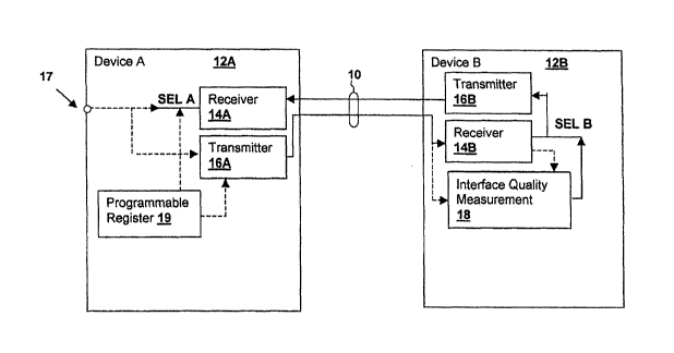
to Figure 1, there is depicted a block diagram of transceivers 12A and 12B
connected by an interface or channel 10 in accordance with an embodiment
of the invention. Transceivers 12A, 12B may be located within a device
such as a computer peripheral, a computer system, or within integrated
circuits interconnected within a system. Interface 10 may be a single two
wire bi-directional interface as depicted, or may be a full-duplex single
wire interface or a bus having multiple transceivers in a half-duplex or
CA 02500465 2005-03-29
WO 2004/042942 PCT/GB2003/004769
full-duplex configuration. Transceivers 12A and I2B connected to interface
each using a receiver 14A and 14B and a transmitter 16A and 16B, but it
should be understood that a receiver or transmitter in accordance with an
embodiment of the invention may be incorporated in devices for connection
to any of the above-specified types of interface I0, as well as other
forms of electrical signal interconnection.
The interface circuits (transmitters 16A,16B and receivers 14A, 14B)
incorporate select inputs SE7~A and SELB that reduce the complexity of the
connected interface circuits, in order to reduce power consumption.
Circuit blocks having lower power consumption may be switched in as
alternatives or circuit blocks may be selectively disabled to reduce the
number of gates, storage circuits, and/or transitions that occur when
processing signals within interface circuits 14A-B and/or 16A-B. Analog
circuit blocks within interface circuits may also be selectively
simplified or eliminated 14A-8 and/or 16A-B when channel conditions
permit.
Thus, the above-described interface circuits provide a selectable
power consumption that can be used to provide lower power usage and
dissipation within transceivers 12A and I2B, when channel conditions are
good, while maintaining low bit error rates (BERs) using a higher power
consumption state when channel conditions are poor. The selection of power
consumption states via select input SELA may be hard-wired or externally
programmed using an external signal terminal 17 or may be programmed using
a bit register 19 within transceiver 12A. Receiver 14A, transmitter 16A or
both may be controlled by one or more selection signals, for example,
multiple bits may be provided for each of transmitter l6A and receiver I4A
so that power consumption may be very finely traded off for receiver
processing power or transmitter signal strength, etc. Alternatively, a
single bit or external terminal may be used to set a single binary power
consumption selection for both transmitter 16A and receiver 14A.
Transceiver 12A is an example of a transceiver having external
selection via register programming or external connection. As such, it is
very useful in integrated circuits and systems, including computer
systems, communication systems, or peripherals where external terminal 17
can be hard-wired depending on the application (e. g., known short shielded
cable length attached to a peripheral dictates a high channel quality or
CA 02500465 2005-03-29
WO 2004/042942 PCT/GB2003/004769
6
connection of two transceivers on a high-quality circuit board also
dictates high channel quality).
Transceiver 12B is an example of a transceiver having automatic
channel-quality-based complexity selection in response to a measurement
performed by interface quality measurement block 18, which may be an
eye-diagram circuit, an error detection circuit or other mechanism for
detection that the channel quality is less than a desired threshold.
Select signal SEL B is provided by an output of interface quality
measurement block 18 and automatically selects higher or lower receiver
and/or transmitter complexity in conformity with the measured channel
quality.
Another type of transceiver power consumption control is provided by
an interface link wherein a register such as programmable register 19 may
be set via reception of a command code sent over interface 10 and received
by a receiver such as receiver 14A. The interface link control is very
useful where the receiver and transmitter characteristics must match (such
as when the select signal changes an error-correction length or when
matching filters are used at each end of interface 10). Interface link
control is also useful for informing a transceiver about channel
conditions when the transceiver being programmed has no ability to
determine the channel quality or does not have information regarding
channel conditions (such as cable length).
Referring now to Figure 2, details of a transceiver 20 in accordance
with an embodiment of the invention are depicted. An interface signal is
received at RX Data In and provided to a receiver circuit 21 that may
contain an equalization filter 21A or may not. The output of receiver
circuit 21 is generally presented to a series of sampling latches 24 and
data is provided from sample latches 24 to a sample memory 25. Sampling
latches 24 and sample memory 25 are used to "oversample" the received
signal so that the edges of the signal can be determined with more
accuracy in the face of high frequency fitter.
Edge detection logic 26 detects one or both edges of the received
signal (which typically contains clock and data bits) and provides
early/late information to phase control 27, which in turn controls
sampling latches 24 to compensate for low-frequency fitter. Data is
CA 02500465 2005-03-29
WO 2004/042942 PCT/GB2003/004769
7
extracted by data selection 28 and error detection and correotion circuits
29 may be employed to further minimize the BER of the received signal.
A digital complexity control circuit 23 provides one or more control
signals to various of the above-described blacks to select a higher or
lower power consumption depending on the channel requirements. The
selection may be static or static/programmable as described above with
respect to Figure 1, or dynamic based upon an output of eye measurement
diagram circuit 22 (or other suitable indicator of channel quality). Eye
measurement diagram provides a measurement of the signal quality output of
receive circuitry 21, giving an indicator of the impact of fitter on BER.
The power consumption of the various circuits is tailored by reducing the
overall complexity or direct power levels used by the circuits and may be
controlled by individual control bits or a single control bit. For
example, the number of sampling latches 24 employed is proportional to the
power consumption of the sampling 24 latches block, the size of sample
memory 25, the resolution of the phase control circuit 27 and edge
detection logic 27, and the depth of error correction and detection 29 are
all proportional to their power consumption. Any or all of the
above-listed circuit blocks may have selectable power consumption and may
be controlled independently or together at one or more power consumption
levels.
The transmitter portion of transceiver 20 comprises an optional
error correction coding circuit 31, an optional equalization filter 32 and
a driver 33 for transmitting data on the interface TX Data Out. Digital
complexity control 23 may also control the complexity of the transmitter
circuits, such as driver 33 current, equalization filter 32 length or ECC
coding 31 depth.
Digital complexity control 23 is also shown coupled to an optional
remote complexity control link 34 for controlling power consumption. A
command received at RX Data In can be received and decoded to control the
complexity of the circuit blocks within transceiver 20 via the output of
data selection 28. Digital complexity control is also shown coupled to the
transmitter circuits for transmitting complexity control information to a
remote transceiver. These remote control features are optional and their
implementation depends on whether it is possible and desirable to send and
receive control information over the interface channel.
CA 02500465 2005-03-29
WO 2004/042942 PCT/GB2003/004769
8
Referring now to Figure 3, techniques for controlling power
consumption within the interface circuits of Figure 2 is illustrated.
Select PD can be used to control power supplied to blocks having power
supplies connected through power control transistor 39 or an equivalent
device, /Select CLK disables a clock via NAND gate 37A or equivalent
device which serves as a clock disable circuit, and /Select RST holds
registers 37B in a reset condition. Sel selects between complex block 37
and alternate block 38 (which generally will be disabled when complex
block 37 circuits are enabled). The circuits shown in Figure 3 are
illustrative and are not typical of the transceiver circuits described
above, which contain a greater number of registers and gates. But the
techniques illustrated can be applied together or selectively to disable
power consumption within the complex portions of the above-described
receivers. Since eliminating clocks or state changes in modern digital
circuits may have the same effect on power consumption as removing power
as long as leakage paths are not present, any of the above techniques may
be sufficient. Another power reduction mechanism is the simplification of
state machine circuits, wherein alternative state machines may be selected
similarly to the selection between complex block 37 and alternate block 38
or by disabling some of the state registers (and changing the
combinatorial feedback logic accordingly).
Referring now to Figure 4, a control method in acoordance with an
embodiment of the present invention is shown in a flowchart. First,
interface channel quality is measured (step 40) and if the interface
channel quality is sufficient to support a lower power consumption state
within the transceiver (decision 41), the lower transceiver complexity is
selected (step 42) and the selection information is optionally transmitted
over the interface to any connected remote transceivers (step 43). The
above-illustrated method includes optional steps 40 and 43, to illustrate
a complete functionality including autonomic measurement and optional
remote control of remote transceivers. However, it should be understood
that those optional steps are not necessary for the practice of the
invention.