Note: Descriptions are shown in the official language in which they were submitted.
CA 02500533 2005-03-29
WO 2004/068731 PCT/US2004/002055
1
MIXED TECHNOLOGY MEMS/SiGe BiCMOS DIGITIZING ANALOG
FRONT END WITH DIRECT RF SAMPLING
FIELD OF THE INVENTION
[0001] The present invention relates to protection of analog to digital
converters
(ADC), to the reduction of power consumption and to the maintenance of high
signal
quality in a radio receiver's analog front end in the presence of large
interfering and
jamming signals. More particularly, the invention relates to a single chip
receiver
utilizing micro electromechanical system (MEMS) technology to receive wideband
or
spread-spectrum signals in a jamming environment with a low resolution ADC,
such as
in a Global Positioning System (GPS) receiver.
BACKGROUND OF THE INVENTION
[0002] This invention is applicable to all communication systems. A spread-
spectrum system will be used to illustrate its use and effectiveness. Spread-
spectrum
communication systems transmit information digitally on a carrier that has
been
modulated with a high-rate pseudorandom binary sequence. The spectrum of the
resulting signal occupies a large bandwidth and appears noise-like. The signal
is subject
to intentional or unintentional jamming. Jamming occurs by transmission of
large radio
frequency signals in nearby or coincident radio spectrum. Jamming signals
located out of
the desired signal's band are usually removed using a preselector filter.
Thus, it is the in-
band signals that present the greater obstacle to accurate reception of the
transmitted
signal.
[0003] Suppressing these interferences can be accomplished with the use of RF
notch filters. When implemented with MEMS technology, this is a low cost, low
power
CA 02500533 2005-03-29
WO 2004/068731 PCT/US2004/002055
2
solution and low distortion for interference suppression. A notch filter is
particularly
effective in suppressing continuous wave (CW) or narrowband interferers. After
these
interferers are removed, the receiver can process the spread spectrum signal
as if the
interference is absent with a small loss, proportional to the bandwidth being
removed.
For interference-free spread spectrum signals the received signal can be
processed with a
very low resolution ADC. For example a 1-bit ADC has a degradation of 1.059 dB
with
baseband I and Q sampling or 1.96 dB with intermediate frequency (IF) sampling
against
Additive White Gaussian Noise (AWGN). A 2-bit ADC has a 0.55 dB degradation
with
baseband I and Q sampling or 0.96 dB with IF sampling. Therefore, to maintain
good
performance with a low ADC complexity and low power consumption, a method of
eliminating the jammers from the received signal should be used.
[0004] Another effect on system design and system performance in a jamming
environment is in power consumption and signal distortion. Ina jamming
environment
when the j amming signals are not removed near the antenna, the components in
the
analog front end must be designed with high linearity at the cost of
significantly higher
power consumption. Also, the presence of large signals puts greater demands on
the
phase noise requirements of the system. To decrease both the high linearity
and phase
noise requirements, it is necessary to remove the jammers before these
components.
[0005] Analog excision methods can eliminate both narrow and wideband
jamming signals using passive components. However, since the jamming signals
can be
located anywhere within the passband, some method for steering, inserting, and
removing the excising circuitry from the signal path must be used. Generally,
filtering
techniques implemented in current receivers use semiconductor switching, e.g.,
semiconductor transistors, to alter the filters' characteristics. The filters'
characteristics
may be altered by switching in different components (e.g., banks of
capacitors) or
different filters altogether. Semiconductor switching, due to the
semiconductor's limited
isolation characteristics, may allow parasitic capacitances from non-selected
filters
CA 02500533 2010-05-04
3
and/or components to effect the performance of a selected filter, resulting in
distortion of he filtered signal.
[0006] From the discussion above, it is apparent that there is a need in the
art for a low power, low distortion mechanism for protecting a receiver's
front end
for use in multiple applications.
SUMMARY OF THE INVENTION
[0007] In the light of the foregoing, the invention relates to an integrated
circuit digitizing analog front end for a receiver, which includes a
substrate; a low
noise amplifier (LNA) on the substrate; an analog-to-digital converter (ADC)
on the
substrate; a plurality of micro electro mechanical system (MEMS) switches on
the substrate; at least one anti-alias filter on the substrate; and at least
one anti jam
filter on the substrate, wherein the filter characteristics of the at least
one anti jam
filter and the at least one anti-alias filter are changed using at least one
of the
plurality of MEMS switches.
[0007a] Accordingly, in one aspect of the present invention there is provided
an Integrated circuit digitizing analog front end (DAFE) for a receiver,
comprising:
a substrate;
a low noise amplifier (LNA) on the substrate;
an analog-to-digital converter (ADC) on the substrate;
a plurality of micro electro mechanical system (MEMS) switches on
the substrate;
at least one anti-alias filter on the substrate; and
at least one anti jam filter on the substrate;
wherein the filter characteristics of the at least one anti jam filter are
changed using at least one of the plurality of MEMS switches, and
wherein the at least one anti jam filter has a filter section comprising a
filter bank and a MEMS switch having a first normally open pole, a second
normally
open pole and a third normally closed pole, and wherein the filter section is
adapted
CA 02500533 2010-05-04
3a
such that the filter bank may be removed from the filter by closing the third
pole and
by opening the first and second poles.
[0007b] According to another aspect of the present invention there is provided
an integrated circuit digitizing analog front end (DAFE) for a receiver,
comprising:
a substrate;
a low noise amplifier (LNA) on the substrate;
an analog-to-digital converter (ADC) on the substrate;
a plurality of micro electro mechanical system (MEMS) switches on
the substrate, wherein each of the plurality of MEMS switches comprises at
least one
pole operative to positively couple and decouple an input of the MEMS switch
to an
output of the MEMS switch;
at least one anti-alias filter on the substrate; and
at least one anti jam filter on the substrate;
wherein the filter characteristics of at least one of the at least one anti-
jam filter and the at least one anti-alias filter are changed using at least
one of the
plurality MEMS switches.
[0008] To the accomplishment of the foregoing and related ends, the
invention, then, comprises the features hereinafter fully described and
particularly
pointed out in the claims. The following description and the annexed drawings
set
forth in detail certain illustrative embodiments of the invention. These
embodiments
are indicative, however, of but a few of the various ways in which the
principles of
the invention may be employed. Other objects, advantages and novel features of
the
invention will become apparent from the following detailed description of the
invention when considered in conjunction with the drawings.
BRIEF DESCRIPTION OF THE DRAWINGS
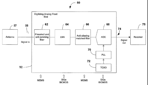
[0009] Fig. 1 is a block diagram of a digitizing analog front end (DAFE) in
accordance with an embodiment of the invention.
CA 02500533 2005-03-29
WO 2004/068731 PCT/US2004/002055
4
[00010] Fig. 2A is an anti-jam filter implemented using a sub-band bandpass
approach in accordance with an embodiment of the invention.
[00011] Fig. 2B illustrates the loss incurred by summing the outputs of many
sub-
band filters with errors uniformly distributed between -(D and degrees.
[00012] Fig. 3 is an anti jam filter implemented using a notch filter approach
in
accordance with another embodiment of the invention.
DETAILED DESCRIPTION OF THE INVENTION
[00013] The following is a detailed description of the present invention with
reference to the attached drawings, wherein like reference numerals will refer
to like
elements throughout.
[00014] Referring now to Fig. 1, a digitizing analog front end (DAFE) 50 in
accordance with one embodiment of the present invention is illustrated. An
antenna or
antenna array 57 for receiving a composite radio signal is connected to an
input port 58
of the DAFE 50. Upon entering the DAFE 50, the composite signal enters a pre-
selector
and anti jamming filter (PS/AJ) 62 for pre-selection of the desired frequency
band and
for excision of narrow band jammers. The output of the PS/AJ filter 62 is
electrically
connected to the input of a low noise amplifier (LNA) 64. The pre-selection
portion of
the PS/AJ filter 62 provides coarse filtering to reduce saturation of the LNA
64 by out of
band jamming, co-site or ambient signals.
[00015] The output of the LNA is electrically connected to the input of an
anti-
aliasing matched filter 66. The output of the anti-aliasing matched filter 66
is electrically
connected to the input of an analog-to-digital converter (ADC) 68, such as a
direct
sampling/under sampling ADC, for example. The anti-aliasing matched filter 66
has a
cutoff frequency that attenuates unwanted signals from the ADC input to the
point that
CA 02500533 2005-03-29
WO 2004/068731 PCT/US2004/002055
they will not adversely affect the circuit. A supporting phase-locked loop
(PLL) 70 and
temperature compensated crystal oscillator (TCXO) 72 provide timing signals
for the
ADC 68. The ADC 68 provides an output 74 of the DAFE 50, which may be
connected
to a receiver 75, such as a GPS receiver, for example.
5
[00016] The implementation of a direct sampling/under sampling ADC 68 can
reduce the complexity of the overall DAFE 50. By performing bandpass sampling,
the
receiver design is simplified by eliminating one or more stages of mixers,
thus reducing
the circuit size and power requirements. Furthermore, the signal quality
increases
through direct in-phase and quadrature-phase projection by avoiding amplitude
and phase
offsets inherent in quadrature demodulation.
[00017] The DAFE 50 preferably employs mixed technology, including Micro
Electro Mechanical System (MEMS) technology and, for example, BiCMOS
technology
on a single substrate 92. In particular, the PS/AJ filter 62 and the anti-
aliasing matched
filter 66 are implemented using MEMS technology, while the LNA 64, ADC 68 and
PLL
70 may be implemented using SiGe BiCMOS technology, for example. The benefits
of a
mixed technology approach include a reduction in size and in power consumption
of the
DAFE 50. Size reduction is a result of the integration of many different
functions onto a
single chip. Power savings results from use of a power efficient SiGe BiCMOS
process,
the use of an under sampling ADC, and MEMS technology.
[00018) The use of an under sampling ADC 68 allows the elimination of at least
one down conversion stage including mixers and PLLs. The inventors estimate an
additional 40% power savings due to elimination of the down conversion stage.
Further
power savings may be realized through the use of passive, high-Q filtering
elements
using MEMS technology. In particular, MEMS technology allows the creation of
small,
low power, low distortion and j armer resistant filters.
[00019] The structure of the PS/AJ filter 62 is dependent upon the method
chosen
to implement the narrowband jammer excision. Exemplary designs for PS/AJ
filters
CA 02500533 2010-06-14
6
include a sub-band bandpass approach, which will pass only a non jammed
portion of the
signal, and a notch filter approach, which will remove the jammer. Depending
on the
size and complexity of the PS/AJ filter, switchable filter banks may be
employed to
permit the DAFE 50 to detect several different frequency bands. To reduce the
effects of
parasitic capacitance that could be introduced from the presence of the unused
filters,
high isolation MEMS switches are used to disconnect the unused filters from
the circuit.
Additionally, the sub-band approach has the added benefit of eliminating the
need for an
additional anti-aliasing filter'as this function is a natural byproduct of the
sub-band
structure.
[00020] Referring to Fig. 2A, an embodiment using a sub-band bandpass
implementation of the PS/AJ filter is illustrated. The PS/AJ filter 62'
incorporates
MEMS switches 80a-80d for selecting the filtering characteristics of the
filter 62'. A
MEMS switch provides several advantages over a semiconductor switch (e.g.,
semiconductor transistors, pin diodes). In particular, a MEMS switch has a
very low
insertion loss (e.g., less than 0.2 dB at 45 GHz) and a high isolation when
open (e.g.,
greater than 30 dB). In addition, the switch has a large frequency response
and a large
bandwidth compared to semiconductor transistors and pin diodes. These
advantages
provide enhanced performance and control when used in tunable filter designs.
Additional details relating to MEMS switches can be found in U.S. Patent No.
6,046,659.
[00021] The MEMS switches used in the PS/AJ filter 62' are double pole single
throw (DPST) switches (e.g., two isolated switch contacts that open and close
together).
It should be appreciated, however, that other configurations of MEMS switches
may be
utilized and the use of a DPST switch is merely exemplary. Furthermore, Fig.
2A shows
a sub-band bandpass implementation using four MEMS switches and four sub-band
filter
banks. It should be appreciated, however, that implementations of a sub-band
bandpass
filter utilizing more or fewer MEMS switches and/or sub-band filter banks
maybe used,
and such implementations are contemplated to be in the scope of the invention.
CA 02500533 2005-03-29
WO 2004/068731 PCT/US2004/002055
7
[00022] It is noted that control lines to command each MEMS switch to "open"
and "close" are not shown in the diagrams. These control lines, however, would
be
evident to one skilled in the art. The open and close action of each MEMS
switch is
achieved by applying a bias voltage to one or more control terminals of the
MEMS
switch. For example, a single pole MEMS switch may have four terminals, two
terminals for the isolated switch contact, and two terminals for a "control"
connection,
e.g., to command the switch to open and close. When a voltage is applied to
the control
terminals of the MEMS switch, an electrostatic force pulls an armature towards
the
substrate. If the switch is a normally open (N.O.) configuration, then the
isolated switch
contact will close upon the application of the voltage. Conversely, if the
switch is a
normally closed (N.C.) switch, then the isolated switch contact will open upon
application of the voltage. It follows that multiple pole MEMS switches will
have an
additional pair of terminals for each additional pole.
[00023] A first terminal on a first pole 80a1 of a first MEMS switch 80a is
connected to an input node 100. A second terminal on the first pole 80a1 of
the first
MEMS switch 80a is connected to an input terminal of a first sub-band filter
bank 102a.
An output terminal of the first sub-band filter bank 102a is connected to a
first terminal
on a second pole 80a2 of the first MEMS switch 80a. A second terminal on the
second
pole 80a2 of the first MEMS switch 80a is connected to a summing junction 104.
[00024] A first terminal on a first pole 80b1 of a second MEMS switch 80b is
connected to the input node 100. A second terminal on the first pole 80b1 of
the second
MEMS switch 80b is connected to an input terminal of a second sub-band filter
bank
102b. An output terminal of the second sub-band filter bank 102b is connected
to a first
terminal on a second pole 80b2 of the second MEMS switch 80b. A second
terminal on
the second pole 80b2 of the second MEMS switch 80b is connected to the summing
junction 104.
CA 02500533 2005-03-29
WO 2004/068731 PCT/US2004/002055
8
[00025] A first terminal on a first pole 80c1 of a third MEMS switch 80c is
connected to the input node 100. A second terminal on the first pole 80c1 of
the third
MEMS switch 80c is connected to an input terminal of a third sub-band filter
bank 102c.
An output terminal of the third sub-band filter bank 102c is connected to a
first tenninal
on a second pole 80c2 of the third MEMS switch 80c. A second terminal on the
second
pole 80c2 of the third MEMS switch 80c is connected to the summing junction
104.
[00026] A first terminal on a first pole 80d1 of a fourth MEMS switch 80d is
connected to the input node 100. A second terminal on the first pole 80d1 of
the fourth
MEMS switch 80d is connected to an input terminal of a fourth sub-band filter
bank
102d. An output terminal of the fourth sub-band filter bank 102d is connected
to a first
terminal on a second pole 80d2 of the fourth MEMS switch 80d. A second
terminal on
the second pole 80d2 of the fourth MEMS switch 80d is connected to the summing
junction 104. The output 106 of the summing junction 104 is the output of the
filter 62.
[00027] The sub-band bandpass design 62', through each sub-band filter 102a-
102d, divides the signal spectrum into many sub-bands. As illustrated in Fig.
2A, each
filter bank 102a-102d includes a different transfer function to filter
specific frequencies
from the composite signal. Each sub-band can be further divided as required to
achieve a
minimum excisable jammer bandwidth. The output of each fixed-frequency sub-
band
filter 102a-102d is examined for the presence of a jammer through the use of
analog
power detection circuitry (not shown) that is digitally controlled, for
example. Detection
of jammer signals is well known by those skilled in the art and will not be
discussed
herein. If a jammer is not present in a particular frequency band, then the
output of the
fixed frequency sub-band filter is summed with the other sub-band filters. If
a jammer is
detected, however, then the respective MEMS switch for the particular sub-band
filter
102a-102d is opened, thus removing the jammer from the spectrum. As noted
previously, a MEMS switch provides several advantages over a semiconductor
switch,
including low insertion loss and high isolation when the switch is open.
Moreover, the
implementation of mixed technology, e.g., MEMS switches and SiGe BiCMOS on the
CA 02500533 2005-03-29
WO 2004/068731 PCT/US2004/002055
9
same substrate, provides a compact package that consumes less power than
traditional
implementations.
[00028] For example, if a jammer signal were detected at the output of the
fourth
sub-band filter 102d and a jammer signal were not detected at the output of
the remaining
sub-band filters 102a-102c, then the first three MEMS switches 80a-80c would
be closed
allowing the "clean signal" to pass, and the fourth MEMS switch 80d would be
open,
thus blocking the jammer signal. Similarly, if a jammer signal were detected
at the
output of the first sub-band filter 102a, and a jammer signal were not
detected at the
output of the remaining sub-band filters 102b-102d, then the first MEMS switch
80a
would be opened, thus blocking the jammer signal, and the remaining MEMS
switches
80b-80d would be closed allowing the clean signal to pass.
[00029] An inherent problem when using superposition of multiple sub-band
filter
outputs is the introduction of phase errors. Referring to Fig. 2B, a graph 107
illustrating
the loss from phase offsets in sub-band filters is illustrated. In particular,
the graph 107
shows that if the phase error introduced by each filter is randomly
distributed within a
small range, the implementation loss is small. For example, an error
distribution over
50 degrees 108 yields only a 1 dB performance loss.
[00030] Referring to Fig. 3, an alternative embodiment of the PS/AJ filter 62"
using a notch filter design is illustrated. The notch filter approach requires
the design
and fabrication of high-Q MEMS filters that have two degrees of freedom:
variability in
center frequency and stop band bandwidth. In the GPS case, the center
frequency should
be steerable over the 20 MHz GPS bandwidth. Ideally, the notch width should be
adjustable from 0 Hz to 10% of either the clear acquisition (C/A) or precision
(P) code
signal widths, or 200 kHz to 2 MHz, depending on which signal is being used.
[00031] The PS/AJ filter 62" includes four filter sections; a pre-select
filter 110
followed by three filter sections 112, 114, 116, all of which are steerable
and bandwidth-
CA 02500533 2005-03-29
WO 2004/068731 PCT/US2004/002055
adjustable. More or fewer steerable filters may be used. The PS/AJ filter 62"
incorporates a 3-pole MEMS switch having two normally open (N.O.) and one
normally
closed (N.C.) contacts. It should be appreciated that the use of a 3-pole MEMS
switch is
merely exemplary and other configurations of a MEMS switch may be employed.
5
[00032] Referring to the PS/AJ filter 62" of Fig. 3, an anti-alias/pre-select
filter
110 has a first terminal connected to an input node 120 and a second terminal
connected
to node 121. A first terminal on a first N.O. pole 80a1' of a first MEMS
switch 80a' is
connected to node 121. A second terminal on the first pole 80a1' of the first
MEMS
10 switch 80a' is connected to an input terminal of a first filter bank 122a.
An output
terminal of the first filter bank 122a is connected to a first terminal on a
second N.O. pole
80a2' of the first MEMS switch 80a'. A second terminal on the second pole
80a2' of the
first MEMS switch 80a' is connected to node 124. A first terminal on a third
N.C. pole
80a3' of the first MEMS switch 80a' is connected to node 121. A second
terminal on the
third pole 80a3' of the first MEMS switch 80a' is connected to node 124.
[00033] A first terminal on a first N.O. pole 80bl' of a second MEMS switch
80b'
is connected to node 124. A second terminal on the first pole 80b1' of the
second
MEMS switch 80b' is connected to an input terminal of a second filter bai-dc
122b. An
output terminal of the second filter bank 122b is connected to a first
terminal on a second
N.O. pole 80b2' of the second MEMS switch 80b'. A second terminal on the
second
pole 80b2' of the second MEMS switch 80b' is connected to node 126. A first
terminal
on a third N.C. pole 80b3' of the second MEMS switch 80b' is connected to node
124.
A second terminal on the third pole 80b3' of the second MEMS switch 80b' is
connected
to node 126.
[00034] A first terminal on a first N. 0. pole 8Ocl' of a third MEMS switch
80c' is
connected to node 126. A second terminal on the first pole 80cl' of the third
MEMS
switch 80c' is connected to an input terminal of a third filter bank 122c. An
output
terminal of the third filter bank 122c is connected to a first terminal on a
second N.O.
CA 02500533 2005-03-29
WO 2004/068731 PCT/US2004/002055
11
pole 80c2' of the third MEMS switch 80c'. A second terminal on the second pole
80c2'
of the third MEMS switch 80c' is connected to node 128. A first terminal on a
third
N.C. pole 80c3' of the third MEMS switch 80c' is connected to node 126. A
second
terminal on the third pole 80c3' of the third MEMS switch 80c' is connected to
node
128.
[00035] The PS/AJ filter 62" can remove jammer signals through the
manipulation of the variable center frequency and the stop bandwidth. Each
filter bank
122a-122c includes a different transfer function to filter specific jammer
frequencies
from the composite signal. Furthermore, filter segments may be removed from
the filter
by closing the bypass MEMS switches 80a3'- 80c3' and opening the selection
MEMS
switches 80a1'-80c1', 80a2'-80c2'. For example, if a single jammer is present,
one of
the filters 122a-122c is tuned through appropriate methods to create a
passband
surrounding the desired signal, but with a notch present at the location of
the jammer.
The tuning of this filter is accomplished using MEMS switches or other
methods, which
are not described here but are known in the literature. A control signal is
sent to the first
MEMS switch 80a', causing the third N.C. pole 80a3' to open and the first N.O.
pole
80a1' and the second N.O. pole 80a2' to close, thus causing the signal and
jammer to
enter the first filter 122a. The first filter 122a removes some or all of the
jammer and it
allows only the signal and any residual jammer to pass to node 124. If no
other jamming
signal is present and if the first jammer has been sufficiently excised, the
second filter
122b and the third filter 122c are not needed, no control signals are sent to
the second
MEMS switch 80b' and the third ITEMS switch 80c' and the third N.C. pole 80b3'
of the
second MEMS switch 80b' and the third N.C. pole 80c3' of the third MEMS switch
80c'
remain closed and the first and second N.O. poles 80b1', 80b2' of the second
MEMS
switch 80b' and the first and second N.O. poles 80c1', 80c2' of the third MEMS
switch
80c' remain open. The signal at node 124 passes through to node 128. If other
jammers
(up to two more for the exemplary circuit of Fig. 3) are present and must be
excised, or if
additional attenuation of the first jammer is desired, or both, the second and
third filters
122b, 122c are tuned to excise the jammers, and control signals are sent to
the second
CA 02500533 2005-03-29
WO 2004/068731 PCT/US2004/002055
12
MEMS switch 80b' and the third MEMS switch 80c'. Finally, if no jamming signal
is
present, the anti-alias filter 110 is placed in the signal path to allow only
the desired
signal to pass.
[00036] While particular embodiments of the invention have been described in
detail, it is understood that the invention is not limited correspondingly in
scope, but
includes all changes, modifications and equivalents coming within the spirit
and terms of
the claims appended hereto. For example, the implementation of a MEMS filter
has been
discussed herein with reference to the PS/AJ filter 62. It will be
appreciated, however,
that the same principles may be applied to the anti-aliasing filter 66.