Note: Descriptions are shown in the official language in which they were submitted.
CA 02500647 2005-03-30
WO 2004/059751 PCT/US2003/040379
METHODS OF FORMING SEMICONDCUTOR MESA
STRUCTURES INCLUDING SELF-ALIGNED CONTACT
LAYERS AND RELATED DEVICES
Related Applications
The present application claims the benefit of; U.S. Provisional Application
No. 60/435,213 filed December 20, 2002, and entitled "Laser Diode With Self
Aligned
Index Guide And Via"; U.S. Provisional Application No. 60/434,914 filed
December
20, 2002, and entitled "Laser Diode With Surface Depressed Ridge Waveguide";
U.S.
Provisional Application No. 60/434,999 filed December 20, 2002 and entitled
"Laser
Diode with Etched Mesa Structure"; and U.S. Provisional Application No.
60/435,211
filed December 20, 2002, and entitled "Laser Diode With Metal Current
Spreading
Layer." The disclosures of each of these provisional applications are hereby
incorporated herein in their entirety by reference.
The present application is also related to: U.S. Application No.
(Attorney Docket No. 5308-281) entitled "Methods Of Forming Semiconductor
Devices Having SelfAligned Semiconductor Mesas and Contact Layers And Related
Devices" filed concurrently herewith; U.S. Application No. (Attorney
Docket No. 5308-282) entitled "Methods Of Forming Semiconductor Devices
Including Mesa Structures And Multiple Passivation Layers And Related Devices"
filed concurrently herewith; and U.S. Application No. (Attorney Docket
No. 5308-283) entitled "Methods Of Forming Electronic Devices Including
Semiconductor Mesa Structures And Conductivity Junctions And Related Devices"
filed concurrently herewith. The disclosures of each ofthese U.S. Applications
are
hereby incorporated herein in their entirety by reference.
Field Of The Inyention
The present invention relates to the field of electronics, and more
particularly,
to methods of forming electronic semiconductor devices and related structures.
Background Of The Invention
A laser is a device that produces a beam of coherent monochromatic light as a
result of stimulated emission of photons. Stimulated emission of photons may
also
produce optical gain, which may cause light beams produced by lasers to have a
high
CA 02500647 2005-03-30
WO 2004/059751 PCT/US2003/040379
optical energy. A number of materials are capable of producing the lacing
effect and
include certain high-purity crystals (ruby is a common example),
semiconductors,
certain types of glass, certain gases including carbon dioxide, helium, argon
and neon,
and certain plasmas.
More recently, lasers have been developed in semiconducting materials, thus
taking advantage of the smaller size, lower cost and other related advantages
typically
associated with semiconductor devices. In the semiconductor arts, devices in
which
photons play a major role are referred to as "photonic" or "optoelectronic"
devices. In
turn, photonic devices include light-emitting diodes (LEDs), photodetectors,
photovoltaic devices, and semiconductor lasers.
Semiconductor lasers are similar to other lasers in that the emitted radiation
has spatial and temporal coherence. As noted above, laser radiation is highly
.monochromatic (i.e., of narrow band width) and it produces highly directional
beams
of light. Semiconductor lasers may differ, however, from other lasers in
several
respects. For example, in semiconductor lasers, the quantum transitions are
associated with the band properties of materials; semiconductor lasers may be
very
compact in size, may have very narrow active regions and larger divergence of
the
laser beam; the characteristics of a semiconductor laser may be strongly
influenced by
the properties of the junction medium; and for P-N junction lasers, the lacing
action is
produced by passing a forward current through the diode itself. ~verall,
semiconductor lasers can provide very efficient systems that may be controlled
by
modulating the current directed across the devices. Additionally, because
semiconductor lasers can have very short photon lifetimes, they may be used to
produce high-frequency modulation. In turn, the compact size and capability
for such
high-frequency modulation may make semiconductor lasers an important light
source
for optical fiber communications.
In broad terms, the structure of a semiconductor laser should provide optical
confinement to create a resonant cavity in which light amplification may
occur, and
electrical confinement to produce high current densities to cause stimulated
emission
to occur. Additionally, to produce the laser effect (stimulated emission of
radiation),
the semiconductor may be a direct bandgap material rather than an indirect
bandgap
material. As known to those familiar with semiconductor characteristics, a
direct
bandgap material is one in which an electron's transition from the valence
band to the
conduction band does not require a change in crystal momentum for the
electron.
CA 02500647 2005-03-30
WO 2004/059751 PCT/US2003/040379
Gallium arsenide and gallium nitride are examples of direct bandgap
semiconductors.
In indirect bandgap semiconductors, the alternative situation exists; i.e., a
change of
crystal momentum is required for an electron's transition between the valence
and
conduction bands. Silicon and silicon carbide are examples. of such.indirect
semiconductors.
A useful explanation of the theory, structure and operation of semiconductor
lasers, including.optical and, electronic confinement and mirroring, is given
by Sze,
Physics of Semiconductor Devices, 2nd Edition (1981) at pages.704-742, and
these
pages are incorporated entirely herein by reference.
~ As known to those familiar with photonic devices such as LEDs and lasers,
the
frequency of electromagnetic radiation (i.e., the photons) that can be
produced by a
given semiconductor material may be a function of the material's bandgap.
Smaller
bandgaps produce lower energy, longer wavelength photons, while wider bandgap
materials produce higher energy, shorter wavelength photons. For.example, one
semiconductor commonly used for lasers is aluminum indium gallium phosphide
(AIInGaP). Because of this material's bandgap (actually a range of bandgaps
depending upon the mole or atomic fraction of each element present), the light
that
AIInGaP can produce may be limited to the red portion of the visible spectrum,
i.e.,
about 600 to 700 nanometers (nm). In order to produce photons that have
wavelengths in the blue or ultraviolet portions of the spectrum, semiconductor
materials having relatively large bandgaps may be used. Group III-nitride
materials
such as gallium nitride (GaN), the ternary alloys indium gallium nitride
(InGaN),
aluminum gallium nitride (AIGaN) and aluminum indium nitride (AIInN) as well
as
the quaternary alloy aluminum gallium indium nitride (AIInGaN) are attractive
candidate materials for blue and UV lasers because of their relatively high
bandgap
(3.36 eV at room temperature for GaN). Accordingly, Group III-nitride based
laser
diodes have been demonstrated that emit light in the 360-460 nm range.
A number of commonly assigned patents and co-pending patent applications
likewise discuss the design and manufacture of optoelectronic devices. For
example,
U.S. PatentNos..6,459,100; 6,373,077; 6,201,262; 6,187,606; 5,912,477; and
5,416,342 describe various methods and structures for gallium-nitride based
optoelectronic devices., U:S. Patent No. 5,838,706 describes low-strain
nitride laser
diode structures. Published U.S. Application Nos. 20020093020 and 20020022290
describe epitaxial structures for nitride-based optoelectronic devices.
Various metal
CA 02500647 2005-03-30
WO 2004/059751 PCT/US2003/040379
contact structures and bonding methods, including flip-chip bonding methods,
are
described in Published U.S. Application No. 20020123164 as well as Published
U.S.
Application No. 030045015 entitled "Flip Chip Bonding of Light Emitting
Devices
and Light Emitting Devices Suitable for Flip-Chip Bonding"; Published U.S.
Application No. 20030042507 entitled "Bonding of Light Emitting Diodes Having
Shaped Substrates and Collets for Bonding of Light Emitting Diodes Having
Shaped
Substrates", and Published U.S. Application No. 20030015721 entitled "Light
Emitting Diodes Including Modifications for Submount Bonding and Manufacturing
Methods Therefor." Dry etching methods are described in U.S. Patent No.
6,475,889.
Passivation methods for nitride optoelectronic devices are described in U.S.
Application Ser. No. 08/920,409 entitled "Robust Group III Light Emitting
Diode for
High Reliability in Standard Packaging Applications" and Published U.S.
Application
No. 20030025121 entitled "Robust Group III Light Emitting Diode for High
Reliability in Standard Packaging Applications." Active layer structures
suitable for
, use in nitride laser diodes are described in Published U.,S. Application No.
20030006418 entitled "Group III Nitride Based Light Emitting Diode Structures
with
a Quantum Well and Superlattice, Group III Nitride Based Quantum Well
Structures
and Group III Nitride Based Superlattice Structures" and Published U.S.
Application
No. 20030020061 entitled "Ultraviolet Light Emitting Diode." The contents of
all of
the foregoing patents, patent applications and published patent applications
are
incorporated entirely herein by reference as if fully set forth herein.
Moreover, laser diodes may require relatively high current levels to provide
conditions for lasing. Accordingly, non-uniformities in distributions of
current across
an active region of a laser diode may reduce performance thereof.
Summary
According to embodiments of the present invention, methods of forming
semiconductor devices may include forming a semiconductor layer on a
substrate, and
forming a contact layer on the semiconductor layer opposite the substrate.
After
forming the semiconductor layer and the contact layer, the contact layer and
the
semiconductor layer can be patterned such that the semiconductor layer
includes a
mesa having a mesa surface opposite the substrate and mesa sidewalls between
the
mesa surface and the substrate and so that the patterned contact layer is on
the mesa
surface.
CA 02500647 2005-03-30
WO 2004/059751 PCT/US2003/040379
More particularly, the mesa may be configured to provide at least one of
optical confinement or current confinement for a light emitting device in the
patterned
semiconductor layer. Moreover, the mesa sidewalls may be free of the contact
layer.
Patterning the contact layer and the semiconductor layer may include forming
. a mask layer on the contact layer opposite the semiconductor layer, and
etching
portions of the contact layer and the semiconductor layer exposed by the mask
layer.
After patterning the contact layer and the semiconductor layer, a passivation
layer can
be formed on the mesa sidewalk and on the mesa surface so that the passivation
layer
is on at least a portion of the patterned contact layer opposite the patterned
semiconductor layer. Moreover, forming the passivation layer may include
forming
the passivation layer across the contact layer opposite the substrate, and a
via may be
formed in the passivation layer exposing a portion of the contact layer
opposite the
mesa surface. In addition, a metal layer may be formed on the passivation
layer and
on the exposed portions of the contact layer opposite the mesa surface.
The contact layer may substantially cover an entirety of the mesa surface, and
the semiconductor layer may include a P-type layer and an N-type layer wherein
at
least a portion of one of the P-type layer and/or the N-type layer is included
in the
mesa. The semiconductor layer may also include an active layer between the P-
type
layer and the N-type layer, and a second contact layer electrically coupled
with the
mesa may be formed so that the first and second contact layers define an
electrical
path through the P-type layer and the N-type layer. In addition, the N-type
layer may
be between the P-type layer and the substrate, and the P-type layer may be
between
the N-type layer and the contact layer.
The contact layer may be a layer of a metal selected from aluminum, copper,
gold, nickel, titanium, platinum, andlor palladium, and the semiconductor
layer may
include an epitaxial semiconductor material. The semiconductor layer may
include a
Group III-V semiconductor material, and the Group III-V semiconductor material
may be a Group III-nitride semiconductor material.
According to additional embodiments of the present invention, methods for
forming semiconductor devices may include forming a semiconductor structure on
a
substrate wherein the semiconductor structure includes a mesa having a mesa
surface
opposite the substrate and mesa sidewalk between the mesa surface and the
substrate.
A contact layer may be formed on the mesa surface, and a passivation layer may
be
formed on the mesa sidewalls and on a portion of the contact layer opposite
the mesa
CA 02500647 2005-03-30
WO 2004/059751 PCT/US2003/040379
surface. Moreover, the passivation layer may have a via hole therein exposing
a
portion of the contact layer opposite the mesa surface.
The mesa may be configured to provide at least one of optical conf nement or
current confinement for a light emitting device in the semiconductor
structure.
Moreover, the mesa sidewalls maybe free of the contact layer.
The contact layer may substantially cover an entirety of the mesa surface, and
the semiconductor structure may include a P-type layer and an N-type layer
wherein
at least a portion of one of the P-type layer and/or the N-type layer is
included in the
mesa. The semiconductor structure may also include an active layer between the
P-
type layer and the N-type layer. A second contact layer electrically coupled
with the
semiconductor structure may be formed so that the first and second contact
layers
define an electrical path through the P-type layer and the N-type layer. In
addition,
the N-type layer may be between the P-type layer and the substrate, and the P-
type
layer may be between the N-type layer and the contact layer.
A metal layer may also be formed on the passivation layer and on the exposed
portions of the contact layer opposite the semiconductor layer, and the
contact layer
may comprise a layer of a metal selected from aluminum, copper, gold, nickel,
titanium, platinum, and/or palladium. Moreover, the semiconductor layer may
include an epitaxial semiconductor material such as a Group III-V
semiconductor
material, and more particularly, a Group III-nitride semiconductor material.
According to still additional embodiments of the present invention, methods of
forming a semiconductor device may include forming a semiconductor structure
on a
substrate wherein the semiconductor structure includes a mesa having a mesa
surface
opposite the substrate and mesa sidewalls between the mesa surface and the
substrate.
In addition, a contact layer may be formed substantially covering an entirety
of the
mesa surface opposite the substrate. A passivation layer may also be formed on
the
mesa sidewalls .and on a portion of the contact layer opposite the mesa
surface
wherein the passivation layer has a via hole therein so that a portion of the
contact
layer opposite the mesa surface is free of the passivation layer. A metal
layer may
also be formed on the passivation layer and on the portion of the contact
layer free of
the passivation layer,
More particularly, the mesa may be configured to provide at least one of
optical confinement or current confinement for a light emitting device in the
semiconductor structure. 'The mesa sidewalls may also be free of the contact
layer.
CA 02500647 2005-03-30
WO 2004/059751 PCT/US2003/040379
In addition, the semiconductor structure may include a P-type layer and an N-
type layer wherein at least a portion of one of the P-type layer and/or the N-
type layer
is included in the mesa. The semiconductor structure may further include an
active
layer between the P-type layer and the N-type layer, and a second contact
layer
electrically coupled with the semiconductor structure may be formed so that
the first
and second contact layers define an electrical path through the P-type layer
arid the N-
type layer. Moreover, the N-type layer may be between the P-type layer and the
substrate, and the P-type layer may be between the N-type layer and the
contact layer.
The contact layer may include a layer of a metal selected from aluminum,
copper, gold, nickel, titanium, platinum, and/or palladium, and the
semiconductor
layer,may include an epitaxial semiconductor material such as a Group III-V
semiconductor material, and more particularly, a Group III-nitride
semiconductor
material.
According to yet additional embodiments of the present invention, a
semiconductor device may include a semiconductor structure on a substrate
wherein
the semiconductor structure includes a mesa having a mesa surface opposite the
substrate and mesa sidewalls between the mesa surface and the substrate. A
contact
layer may be included on the mesa surface, and a passivation layer may be
included
on the mesa sidewalls and on a portion of the contact layer opposite the mesa
surface.
In addition, the passivation layer may have a via hole therein exposing a
portion of the
contact layer opposite the mesa surface.
The mesa may also be configured to provide at least one of optical
confinement or current confinement for a light emitting device in the
semiconductor
structure. In addition, the mesa sidewalls may be free of the contact layer.
The contact layer may substantially cover an entirety of the mesa surface, and
the semiconductor structure may include a P-type layer and an N-type layer
wherein
at least a portion of one of the P-type layer and/or the N-type layer is
included in the
mesa. The semiconductor structure may also include an active layer between the
P-
type layer and the N-type layer. In addition, a second contact layer may be
electrically coupled with the semiconductor structure so that the first and
second
contact layers define an electrical path through the P-type layer and the N-
type layer.
Furthermore, the N-type layer may be between the P-type layer and the
substrate, and
the P-type layer may be between the N-type layer and the contact layer.
CA 02500647 2005-03-30
WO 2004/059751 PCT/US2003/040379
In addition, a metal layer may be provided on the passivation layer and on the
exposed portions of the contact layer opposite the semiconductor layer, and
the
contact layer may include a layer of a metal selected from aluminum, copper,
gold,
nickel, titanium, platinum, and/or palladium. The semiconductor layer may
include
an epitaxial semiconductor material such as a Group III-V semiconductor
material,
and more particularly, a Group III-nitride semiconductor material.
According to more embodiments of the present invention, a semiconductor
device may include a semiconductor structure on a substrate wherein the
semiconductor structure includes a mesa having a mesa surface opposite the
substrate
and mesa sidewalls between the mesa surface and the substrate. A contact layer
may
substantially cover an entirety of the mesa surface opposite the substrate.
The mesa may also be configured to provide at least one of optical
confinement or current confinement for a light emitting device in the
semiconductor
structure. Moreover, the mesa sidewalk may be free of the contact layer.
In addition, a passivation layer may be provided on the mesa sidewalk and on
a portion of the contact layer opposite the mesa surface wherein the
passivation layer
has a via hole therein expos'irig a portion of the contact layer opposite the
mesa
surface. A metal layer may also be provided on the passivation layer and on
the
exposed portion of the contact layer opposite the semiconductor layer.
The semiconductor structure may include a P-type layer and an N-type layer
wherein at least a portion of one of the P-type layer and/or the N-type layer
is
included in the mesa. . The semiconductor structure may further include an
active
layer between the P-type layer and the N-type layer. In addition, a second
contact
layer may be electrically coupled with the semiconductor structure so that the
first and
second contact layers define an electrical path through the P-type layer and
the N-type
layer. More particularly, the N-type layer may be between the P-type layer and
the
substrate, and the P-type layer may be between the N-type layer and the
contact layer.
The contact layer may include a layer of a metal selected from aluminum,
copper, gold, nickel, titanium, platinum, and/or palladium, and the
semiconductor
layer may include an epitaxial semiconductor material such as a Group III-V
semiconductor material, and more particularly, a Group III-nitride
semiconductor
material.
CA 02500647 2005-03-30
WO 2004/059751 PCT/US2003/040379
Brief Description Of The Drawings
Figure 1 is a cross-sectional view illustrating a mesa structure for a
semiconductor laser.
Figure 2 is a cross-sectional view illustrating semiconductor structures
according to embodiments of the present invention.
Figure 3 is a scanning electron microscope (SEM) photomicrograph of a
cross-section of a semiconductor structure according to embodiments of the
present
invention.
Figures 4A-E are cross-sectional views illustrating steps of forming
semiconductor structures according to embodiments of the present invention.
Detailed Description
The present invention will now be described more fully hereinafter with
reference to the accompanying drawings, in which preferred embodiments of the
invention are shown. The invention may, however, be embodied in different
forms
and should not be construed as limited to the embodiments set forth herein.
Rather,
these embodiments are provided so that this disclosure will be thorough and
complete,
and will fully convey the scope of the invention to those skilled in the art.
In the
drawings, the thickness of layers and regions are exaggerated for clarity. It
will also
be understood that when a layer is referred to as being "on" another layer or
substrate,
it can be directly on the other layer or substrate, or intervening layers may
also be
present. It will also be understood that when an element is referred to as
being
"coupled" or "connected" to another element, it can be directly coupled or
connected ..~
to the other element, or intervening elements may also be present. Like
numbers refer
to like elements throughout. Furthermore, relative terms such as "vertical"
and
"horizontal" may be used herein to describe a relationship with respect to a
substrate
or base layer as illustrated in the figures. It will be understood that these
terms are
intended to encompass difFerent orientations of the device in addition to the
orientation depicted in the figures.
Group III-nitride materials may be made P-type by doping with P-type
impurities (dopants) such as magnesium. However, P-type nitride semiconductor
materials may provide relatively low carrier activation rates and relatively
low carrier
mobilities. Accordingly, P-type nitride semiconductor materials may be
characterized.
by relatively high resistivities. Because laser diodes may require relatively
high
CA 02500647 2005-03-30
WO 2004/059751 PCT/US2003/040379
current levels to provide conditions for lasing, it may be beneficial for the
ohmic
contact to the P-type nitride material to cover as much surface area as
possible.
Figure 1 is cross-sectional view illustrating a structure providing an ohmic
contact to a P-type Group III-nitride based laser diode. As shown in Figure l,
a laser
5 structure 210 includes a substrate 212 on which is formed an epitaxial
semiconductor
structure 214 comprising one or more Group III-nitride materials. The
epitaxial
semiconductor structure 214 may include an N-type layer 215, a P-type layer
217, and
an active layer 216 between the N-type and P-type layers. The active layer 216
may
include any of a number of different structures and/or layers and/or
combinations
10 thereof, such as single or multiple quantum wells, double heterostructures,
and/or
superlattices. Active layer 216 may also include light and current confinement
layers
that may encourage laser action in the device.
Portions of the epitaxial structure 214 may be patterned into a mesa structure
220 for optical and current confinement purposes. A passivation layer 218 may
protect and insulate exposed surfaces of the P-type layer 217. The passivation
layer
218 may be a layer of an insulating material such as silicon dioxide, silicon
nitride,
aluminum oxide, and/or combinations thereof
The laser structure 210 may include a first ohmic contact layer 226 on the P-
type layer 217 and a second ohmic contact layer 227 on the substrate 212
opposite the
epitaxial semiconductor structure 214. A metal overlayer 224 may be provided
on the
passivation layer 218 and on the first ohmic contact layer 226 to provide a
conductive
path for interconnection of the device 210 with an external circuit.
While the second ohmic contact 227 is shown on the substrate 212, the ohmic
contact 227 may be provided on the N-type layer 215. In the device illustrated
in
Figure l, the substrate 212 may comprise a conductive material such as N-type
silicon
carbide to provide a "vertical" device having a "vertical" current path
between the first
and second ohmic contacts 226 and 227 through the epitaxial semiconductor
structure
214 and the substrate 212. Stated in other words, the anode and cathode of the
device
are on opposite sides of the substrate 212. In a "horizontal" device, for
example, the
second ohmic contact could be placed on an exposed portion of the N-type layer
215
so that both ohmic contacts are on the same side of the substrate.
As shown in Figure 1, the ohmic contact 226 on the P-type layer 217 can be
formed within a via 222 that has been opened through the passivation layer 218
to
expose a portion of the surface 220A of the mesa 220. More particularly, the
mesa
CA 02500647 2005-03-30
WO 2004/059751 PCT/US2003/040379
11
220 can be fabricated by forming an epitaxial semiconductor layer, forming a
photoresist layer on the epitaxial semiconductor layer, patterning the
photoresist layer
to expose portions of the semiconductor layer (using a technique known as
photolithography), and etching the exposed portions of the epitaxial
semiconductor
layer to form the mesa 220. The epitaxial semiconductor layer can be etched
using a
. dry etch in an argon (Ar) environment using an etchant including chlorine
(C12).
More particularly, a dry etch for the epitaxial semiconductor layer may
include
flowing argon (Ar) at a rate in the range of approximately 2-40 sccm and
flowing
chlorine (C12) at a rate in the range of approximately 5-50 sccm in a reactive
ion etch
(RIE) reactor at a pressure in the range of approximately 5-50 mTorr and at a
radio
frequency (RF) power in the range of approximately 25-1000 W.
The epitaxial semiconductor..structure 214 including the mesa 220 is then
covered with the passivation layer 218, and a second patterned photoresist
layer can
be formed and patterned (using photolithography) on the passivation layer to
expose a
portion of the passivation layer where the via is to be formed. The exposed
portion of
the passivation layer can then be etched to form the via 222 exposing a
portion of the
mesa surface 220A.
A layer of a metal such as nickel, titanium, platinum, palladium, andlor
combinations thereof can then be deposited on the portion of the mesa surface
220A
exposed by the via 222. Because of tolerance limits of the two
photolithography steps
discussed above, however, it may be difficult to align the via 222 with the
mesa
surface 220A. Accordingly, the via 222 may need to be patterned to be
significantly
narrower than the mesa surface 220A so that the passivation layer 218 may
extend
onto significant portions of the mesa surface 220A and so that the ohmic
contact 226
may not contact significant portions of the mesa surface 220A. Accordingly,
electric
current passing from the ohmic contact 226 to the mesa surface 220A may be
distributed unevenly across the mesa and performance ofthe device may be
degraded.
As shown in Figure 1, the passivation layer 218 may cover corners 211 of the
mesa 220. The corners 211 may be electrically vulnerable regions of the
structure,
and the passivation layer may provide protection therefor. More particularly,
it may
be desirable to protect the mesa corners 211 when the metal overlayer 224 is
deposited. If the corners are not protected when the metal overlayer 224 is
deposited,
metal from the overlayer may migrate down the mesa 220 sidewalk which may
cause
current leakage, electrical short circuits, and/or an increase in a lasing
threshold
CA 02500647 2005-03-30
WO 2004/059751 PCT/US2003/040379
12
voltage and/or current. Providing portions 228 of the passivation layer 218 on
the
corners 211 of the mesa 220A may also protect mesa sidewalls from
environmental
conditions such as high~humidity.
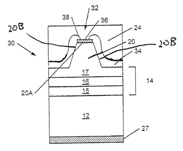
A laser diode structure according to embodiments of the present invention is
illustrated in the cross-sectional view of Figure 2. The laser diode structure
may
include a substrate 12, an epitaxial semiconductor structure 14, ohmic contact
layers
36 and 27, a passivation layer 34, and a metal overlayer 24. Moreover, the
epitaxial
semiconductor structure 14 may include a Group III-V compound semiconductor
material such as a Group III-nitride compound semiconductor material. The
ohmic
contact layers 36 and 27 may each comprises a layer of a metal such as
aluminum,
copper, gold, nickel (Ni), titanium (Ti), platinum (Pt), and/or palladium
(Pd). The
metal overlayer 24 may comprise.a layer of a metal such as nickel (Ni), gold
(Au),
platinum (Pt), titanium (Ti), tungsten (W), molybdenum (Mo); tantalum (Ta),
and/or
palladium (Pd).
In some embodiments, the substrate 12 may include substrate materials such
as N-type silicon carbide having a polytype such as ZH, 4H, 6H, 8H, 15R,
and/or 3C;
sapphire; gallium nitride; and/or aluminum nitride. Moreover, the substrate 12
may
be conductive to provide a "vertical" device having a "vertical" current flow
through
the epitaxial semiconductor structure 14 and the substrate 12. In an
alternative, the
substrate 12 may be insulating or semi-insulating where both ohmic contacts
are
provided on a same side of the substrate to provide a "horizontal" device. A
conductive substrate could also be used in a "horizontal" device. Moreover,
the term
substrate may be defined to include a non-patterned portion of the
semiconductor
material making up the semiconductor structure 14, and/or there may not be a
material
transition between the substrate 12 and the semiconductor structure 14.
Portions of the epitaxial semiconductor structure 14 may be patterned into a
mesa stripe, for example, to provide optical and/or current confinement. As
shown,
only a portion of the epitaxial semiconductor structure 14 is included in the
mesa 20.
For example, the epitaxial semiconductor structure 14 may include N-type and P-
type
layers and portions of one or both of the N-type and P-type layers may be
included in
the mesa 20. According to particular embodiments, the epitaxial semiconductor
structure 14 may include an N-type layer 15 adj acent the substrate 12 and a P-
type
layer 17 on the N-type layer opposite the substrate 12. The mesa may include
portions of the P-type layer 17 and none of the N-type layer 15 as shown in
Figure 2.
CA 02500647 2005-03-30
WO 2004/059751 PCT/US2003/040379
13
In alternatives, the mesa may include all of the.P-type layer 17 and portions
(but not
all) of the N-type layer; or all of the P-type layer 17 and the N-type layer
15 (such that
sidewalls of the mesa 20 extend to the substrate 12.
The epitaxial semiconductor structure 14 may also include an active layer 16
between the N-type layer 15 and the P-type layer 17. The active layer 16 may
include
a number of different structures and/or layers and/or combinations thereof.
The active
layer 16~ for example, may include single or multiple quantum wells, double
heterostructures, and/or superlattices. The active layer 16 may also include
light
and/or current confinement layers that may encourage laser action in the
device.
By way of example, a uniformly thick layer of epitaxial semiconductor
material may be formed on the substrate 12, and a layer of an ohmic contact
material
may be formed on the layer of the epitaxial semiconductor material. The mesa
20 and
the ohmic contact layer 36 may be formed by selectively etching the layer of
the
contact material and the layer of the epitaxial semiconductor material using
the same
etch mask. Moreover, a height of the mesa 20 may be determined by a depth of
the
etch used to form the mesa 20. According to embodiments of the present
invention,
the mesa etch depth (and resulting mesa thickness) may be in the range of
approximately 0.1 to 5 microns, and according to additional embodiments may be
no
greater than approximately 2.5 microns. In addition, a width of the mesa
surface 20A
between mesa sidewalls 20B may be in the range of approximately 1 to 10
microns or
more. By patterning the ohmic contact layer 36 and the mesa 20 using the same
etch
mask, the ohmic contact layer 36 may substantially cover an entirety of the
mesa
surface 20A between mesa sidewalls 20B. Moreover, the mesa surface 20A may be
a
P-type semiconductor material.
The passivation layer 34 may protect and insulate the epitaxial semiconductor
structure 14 including the mesa 20. The passivation layer 34, for example, may
include a layer of an insulating material such as silicon dioxide, silicon
nitride,
aluminum oxide, and/or combinations thereof, and the passivation layer 34 may
be
formed using a deposition technique such as plasma enhanced chemical vapor ,
deposition~(PECVD), low pressure chemical vapor deposition (LPCVD), chemical
vapor deposition (CVD), sputtering, and/or e-beam evaporation. A via 32
through the
passivation layer 34 may expose a portion of the ohmic contact layer 36, and
the
metal overlayer 24 may contact the ohmic contact layer 36 through the via 32.
As
shown, portions 38 of the passivation layer 34 may overlap peripheral portions
of the
CA 02500647 2005-03-30
WO 2004/059751 PCT/US2003/040379
14
ohmic contact layer 36 opposite the mesa surface 20A, and portions of the
ohmic
contact layer 36 exposed by the via 32 may be free of the passivation layer
34.
Figure 3 is a scanning electron microscope (SEM) micrograph of a
semiconductor structure according to embodiments of the present invention. As
shown, the semiconductor structure includes a substrate 12°, an
epitaxial
semiconductor structure 14' including a mesa 20' having a mesa surface 20A',
an
ohmic contact layer 36', a passivation layer 34', and a metal overlayer 24'.
As shown y
in Figure 3, the epitaxial semiconductor structure 14' may include an N-type
layer 15'
and a P-type layer 1T, and sidewalls 20B' of the mesa 20' may extend to the
substrate
12' so that all of the epitaxial semiconductor structure 14' is included in
the mesa 20'.
The passivation layer 34' may be a layer of silicon nitride that may provide
protection and insulation for exposed surfaces of the epitaxial semiconductor
structure
14' including mesa 20'. Via 32' through the passivation layer 34' may expose a
portion of the ohmic contact layer 36' so that the exposed portion of the
ohmic contact
layer 36' is free of the passivation layer 34'. The metal overlayer 24'
contacts the
ohmic contact layer 36' through the via 32'. Portions 38' of the passivation
layer 34'
overlapping peripheral portions of the ohmic contact layer 36' may provide
protection
for the peripheral portions of the ohmic contact layer 36' and corner portions
of the
mesa 20' wherein the mesa surface 20A' and the mesa sidewalls 20B' meet.
Because the ohmic contact layer 36' may cover substantially an entirety of the
mesa surface 20A' between mesa sidewalls 20B', electric current passing
between the
metal overlayer 24' and the mesa 20' may be spread substantially over an
entirety of
the width of the mesa surface 20A' between mesa sidewalls 20B' using the ohmic
:..~
contact layer 36' without using a current spreading layer in the P-type layer
1T. In
other words, the ohmic contact layer 36' may act as a current spreading layer
thereby
improving current-carrying characteristics of the semiconductor device of
Figure 3 by
spreading current outside the P-type layer 17' of mesa 20'. By providing the
ohmic
contact layer 36' as a current spreading layer, current flow through the
epitaxial
region may be improved thereby enhancing light emission from the laser diode.
Steps of forming semiconductor devices according to embodiments of the
present invention are illustrated in Figures 4A-E. As shown in Figure 4A, a
precursor
structure of a semiconductor device, such as a laser diode, may include a
precursor
epitaxial semiconductor layer 114' on substrate 112 and a precursor ohmic
contact
layer 142' on the precursor epitaxial semiconductor layer 114°. The
precursor ohmic
CA 02500647 2005-03-30
WO 2004/059751 PCT/US2003/040379
contact layer 142' may include a metal stack that provides ohmic contact with
the
epitaxial semiconductor layer. In addition to or in an alternative to
providing ohmic
contact with the epitaxial semiconductor layer a metal stack of the precursor
ohmic
contact layer 142' may also include other layers such as barrier and/or
bonding layers
5 . as described, for example, in Published U.S. Patent Application No.
20030045015
(Ser.No. 10/185,252) and Published U.S. Patent Application No. 20030042507
(Ser.No. 10/185,350), the disclos»res of which are hereby incorporated herein
in their
entirety by reference.
A mask 144 can be provided on the precursor ohmic contact layer 142' so that
10 portions of the precursor ohmic contact layer 142' and the precursor
epitaxial
semiconductor layer 114' are free of the mask layer. For example, the mask 144
may
be a photoresist mask that is patterned using photolithographic techniques. In
an
alternative, the mask 144 may be a layer of another material that can resist
an etch
chemistry used to etch the precursor ohmic contact layer 142' and the
precursor
15 epitaxial semiconductor layer 114'.
In addition, the precursor epitaxial semiconductor layer 114' may include an
N-type layer adjacent the substrate 112 and a P-type layer on the N-type layer
opposite the substrate 112. The precursor epitaxial semiconductor layer 114'
may
also include an active layer between N-type and P-type layers. An active
layer, for
example, may include a number of different structures and/or layers and/or
combinations thereof. An active layer, for example, may include single or
multiple
quantum wells, double heterostructures, and/or superlattices. An active layer
may
also include light and/or current confinement layers that may encourage laser
action in
the completed device.
Portions of the precursor ohmic contact layer 142' and the precursor epitaxial
semiconductor layer 114' not covered by the mask 144 may be selectively
removed to
provide ohmic contact layer 142 and epitaxial semiconductor layer 114. More
particularly, the epitaxial semiconductor layer 114 may define a mesa 146
having a
mesa surface 146A opposite the substrate and mesa sidewalls 146B between the
mesa
surface 146A and the substrate 112, and the ohmic contact layer 142 may extend
across substantially an entire width of the mesa surface 146A between mesa
sidewalls
146B.
Because the ohmic contact layer 142 and the epitaxial semiconductor layer
114 are patterned using the same mask 144, the ohmic contact layer 142 may be
"self
CA 02500647 2005-03-30
WO 2004/059751 PCT/US2003/040379
16
aligned" with respect to the mesa surface 146A of the mesa 146. Accordingly,
the
ohmic contact layer 142 may extend across substantially an entire width of the
mesa
surface 146A between mesa sidewalls 146B without extending onto mesa sidewalk
146B. The ohmic contact layer 142 may thus spread current across substantially
an
entire width of the mesa surface 146A between mesa sidewalls 146B without
shorting
to mesa sidewalls 146B.
As shown in Figure 4B, the etch depth may be such that the epitaxial
semiconductor layer 114 may be etched to the substrate 112 so that mesa
sidewalls
146B extend to the substrate 112. If the epitaxial semiconductor layer 114
includes
N-type and P-type layers, an entirety of both the N-type and P-type layers may
be
included in the mesa when the mesa sidewalls extend to the substrate. In an
alternative, the semiconductor layer 114 may not be etched completely to the
substrate so that the mesa does not include all of the semiconductor layer. If
the
semiconductor layer includes N-type and P-type layers, a portion of one or
both layers
may be included in the mesa and a portion of one or both layers may be
included in an
unpatterned portion of the semiconductor layer adjacent the substrate.
As shown in Figure 4C, the mask 144 can be removed, and a passivation layer
148 may be formed on the ohmic contact layer 142, on sidewalk of the mesa 146,
and
on the substrate 112. While the passivation layer 148 is shown directly on
portions of
the substrate 112, portions of the epitaxial semiconductor layer 114 may be
between
the passivation layer 148 and the substrate 112 if sidewalls of the mesa 146
do not
extend to the substrate surface. The passivation layer 148 may be a layer of
an
insulating material such as silicon nitride, silicon,dioxide, aluminum oxide,
and/or
combinations thereof, and the passivation layer 148 may be formed using a
deposition
technique such as plasma enhanced chemical vapor deposition (PECVD), low
pressure chemical vapor deposition (LPCVD), chemical vapor deposition (CVD),
sputtering, and/or e-beam evaporation. Moreover, the passivation layer 148 may
be
formed having a~thickness in the range of approximately 0.1 to 2 microns.
A via 150 can then be formed in the passivation layer 148 using
photolithographic patterning techniques to thereby expose a portion 142A of
the
ohmic contact layer 142. Stated in other words, exposed portions 142A of the
ohmic
contact layer 142 are free of the passivation layer 148 after forrriing the
via 150.
Because the ohmic contact layer 142 is patterned before forming the
passivation layer
148, a tolerance for positioning of the via 150 does not affect a tolerance of
an
CA 02500647 2005-03-30
WO 2004/059751 PCT/US2003/040379
17
alignment of the ohmic contact layer 142 with respect to the mesa surface
120A.
Moreover, portions of the passivation layer 148 extending on the ohmic contact
layer
142 adjacent the via 150 may provide protection for corner portions of the
mesa 146.
As shown in Figure 4E, a metal overlayer 152 may be deposited on the
. , passivation layer 148 and on portions of the ohmic contact Iayer 142 free
of the
passivation layer 148. The metal overlayer 150 may be a layer of a metal such
as
nickel, gold, platinum, titanium, molybdenum, tantalum, palladium, and/or
combinations thereof. Accordingly, electrical connection to another device may
be
provided on the metal overlayer 152 at a point relatively remote from the mesa
146.
The resulting semiconductor device may provide an edge emitting
semiconductor laser with light being emitted parallel to the substrate along a
lengthwise direction of a semiconductor mesa stripe. Stated in other words,
the light
may be emitted along a direction perpendicular to the cross section of Figure
4E.
While methods and devices have been discussed with reference to methods of
forming
light emitting devices such as laser diodes, methods according to embodiments
of the
present invention may be used to form other semiconductor devices such as
conventional diodes, conventional light emitting diodes, or any other
semiconductor
device including a semiconductor mesa.
While this invention has been particularly shown and described with reference
to preferred embodiments thereof, it will be understood by those skilled in
the art that
various changes in form and details may be made therein without departing from
the
spirit and scope of the invention as defined by the appended claims and their
equivalents.