Note: Descriptions are shown in the official language in which they were submitted.
CA 02500720 2006-12-29
20365-4942
1
Description
Cover
The invention relates to a cover for a chamber of a
housing of a device, having an approximately plate-like
carrier which bears a conductor track pattern formed as
a punched grid, having a sensor arranged on the
conductor track pattern and a plug holder formed on the
carrier for a device plug for making contact with the
conductor track pattern.
In such a cover, it is known to encapsulate the punched
grid during the production of the carrier by the
plastic injection molding process and subsequently to
divide the connecting points of the punched grid not
belonging to the conductor track pattern.
On account of the high injection pressures which act on
the punched grid in the process, the configuration of
the punched grid must be designed with regard to the
courses of the conductor tracks, the spacings of the
conductor tracks and the connecting points in such a
way that no deformation of the conductor tracks and, at
the same time, displacement of the sensor position and
of the plug contact can occur. These high requirements
necessitate a great deal of effort and lead to
restrictions on the courses of the conductor tracks.
It is therefore an object of embodiments of the
invention to provide a cover of the type mentioned at
the beginning which consists of simple components, can
easily be mounted and ensures a satisfactory function.
CA 02500720 2006-12-29
20365-4942
la
Accordingly, in one aspect of the invention, there
is provided a cover for a chamber of a housing of a device,
having an approximately plate-like carrier which bears a
conductor track pattern formed as a punched grid, having a
sensor arranged on the conductor track pattern and a plug
holder formed on the carrier for a device plug for making
contact with the conductor track pattern, wherein the
punched grid resting on the approximately plate-like carrier
is held by fixing elements and is covered by a covering
connected to the carrier at its circumferential edge.
According to embodiments of the invention, the
above object is achieved in that the punched grid resting on
the approximately plate-like carrier is held by fixing
elements and is covered by a covering connected to the
carrier at its circumferential edge.
CA 02500720 2005-03-31
WO 2004/031558 PCT/DE2003/003006
- 2 -
By means of this construction, the separately produced
punched grid is fitted to the likewise separately
produced carrier and held in its installed position by
the fixing elements. After that, the connecting points
are separated and the covering is fitted.
Since there are no applications of force as a result of
high injection pressures, a few connecting points
suffice. The fixing elements lead to exact positioning
of the conductor tracks and therefore also of the
sensor and the plug-in contacts, so that only small
spacings are needed between the conductor tracks of the
conductor track pattern. Therefore, the overall size
of the cover can also be kept small.
The sensor can be fitted without difficulty before the
punched grid is mounted. This makes it possible to
fabricate the punched grid with the sensor at a
different location from the location of the production
of carrier and covering, so that fabrication can be
carried out more efficiently, more flexibly and more
economically.
Variants of the cover having other dimensions and other
plugs for different devices are easily possible, it
being possible for the basic dimensions for the carrier
to be maintained.
The punched grid can have contact tongues for making
contact with the device plug, which project into the
plug holder.
In this case, the contact tongues can in particular be
parts of the punched grid bent down out of the plane of
the punched grid, reducing the number of components
required.
CA 02500720 2005-03-31
WO 2004/031558 PCT/DE2003/003006
- 2a -
For the purpose of correct positioning of the device
plug in relation to the contact tongues, the plug
holder can be formed in the manner of a sleeve
protruding from the carrier, the plug holder preferably
being formed in one piece with the plug.
CA 02500720 2005-03-31
WO 2004/031558 PCT/DE2003/003006
- 3 -
In order to make further contacts, the carrier plate
can have one or more leadthroughs, through which one or
more further contact tongues projecting on the side of
the carrier plate facing away from the punched grid are
led.
In this case, in order to reduce the components, the
one or more further contact tongues are in particular
parts of the punched grid bent down out of the plane of
the punched grid.
In order to protect the sensor against contamination
and mechanical damage, on its side facing away from the
punched grid the carrier can have a sensor housing,
into which the sensor projects, carrier and sensor
housing preferably being formed in one piece.
The further contact tongues and/or the sensor or the
sensor housing can project into the chamber of the
housing.
For the purpose of protection against environmental
influences in a component-saving manner, the cover is
welded, in particular laser welded, or adhesively
bonded to the carrier at its circumferential edge.
However, it is also possible for the cover to be
connected detachably to the carrier, resting with its
circumferential edge over a circumferential seal on the
carrier and in particular by means of a screw
connection.
Simple, rapid and accurately-positioned mounting is
made possible by the fact that the fixing elements are
latching elements or clamping elements into which the
punched grid can be latched or clamped.
CA 02500720 2005-03-31
WO 2004/031558 PCT/DE2003/003006
- 3a -
In this case, if the latching elements or clamping
elements are formed in one piece with the carrier, this
leads to a reduction in the mounting effort and to
fewer necessary components.
CA 02500720 2005-03-31
WO 2004/031558 PCT/DE2003/003006
- 4 -
The carrier can be a plastic part, in particular a
plastic injection molding, which can be produced simply
and at the same time insulates the conductor tracks
from one another.
This ability to be produced simply is also provided if
the covering is a plastic part shaped like a shell or
pot, in particular a plastic injection molding.
The punched grid can be constructed in different ways.
For example, the punched grid can be punched out from a
metal sheet (lead frame) or from a printed circuit
board bearing conductor tracks.
For the purpose of simple mounting, it can be possible
for the carrier to be connected to the housing by means
of screws, closing the chamber of the housing.
The cover can be used for an extremely wide range of
devices. For example, it can be used on gas pedal
modules. A preferable use is for the device to be a
throttle flap connecting piece for an internal
combustion engine, in particular of a motor vehicle,
and for a continuous throttle opening which can be shut
off by a throttle flap arranged on a throttle flap
shaft to be formed in the housing, an electric-motor
drive, by means of which the throttle flap shaft can be
driven pivotably, in particular via a gearbox being
arranged in the housing.
In this case, the sensor can be a position sensor
registering the position of the throttle flap shaft or
of the gearbox.
Registering the position of the gearbox without contact
is in this case possible in a simple manner if the
sensor is a magnetoresistive sensor or a Hall sensor.
CA 02500720 2005-03-31
WO 2004/031558 PCT/DE2003/003006
_ 5 _
The at least one or further contact tongues can be a
motor plug for making contact with the electric-motor
drive.
Exemplary embodiments of the invention are illustrated
in the drawing and will be described in more detail in
the following text. In the drawing:
figure 1 shows a perspective view of a throttle flap
connecting piece
figure 2 shows a basic exploded illustration of a
housing cover comprising carrier plate,
punched grid and covering
figure 3 shows a perspective view of a punched grid.
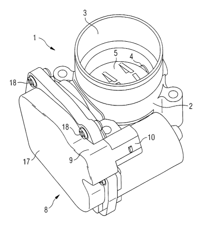
The throttle flap connecting piece 1 illustrated in the
figures has a housing 2 in which a throttle opening 3
is formed. A throttle flap shaft 4 which bears a
throttle flap 5, by means of which the passage cross-
section of the throttle opening 3 can be shut off, is
led transversely through the throttle opening 3.
The two ends of the throttle flap shaft 4 are mounted
in bearing holes in the housing 2 such that they can
rotate. The one free end of the throttle flap shaft 4
projects through a base into a pot-like housing chamber
of the housing 2, of which the outwardly oriented
opening can be closed by a housing cover 8.
In a motor chamber which, at its one end, opens into
the housing chamber, there is arranged an electric
motor, on the motor shaft of which a drive pinion is
seated. The drive pinion drives the throttle flap
shaft 4 rotatably via a gearbox.
CA 02500720 2005-03-31
WO 2004/031558 PCT/DE2003/003006
- 6 -
The housing cover 8 has a plate-like carrier 9, which
is an insulating plastic injection molding, a sleeve-
like plug holder 10 for making contact with a device
plug, a pot-like sensor housing 11 and a further plug
holder 12 of a motor plug, all of which project into
the pot-like housing chamber.
A punched grid 6 is placed on the side of the carrier 9
facing away from the housing chamber and the conductor
tracks 7 of the punched grid 6 are held in their
position by latching elements, not illustrated.
Following this latching fixing of the conductor tracks
7 to the carrier 9, the connecting points 13 of the
conductor tracks 7 of the punched grid 6 are divided.
End regions of the conductor tracks 7 are bent down at
right angles out of the plane of the punched grid 6 and
form contact tongues 14, which project through
corresponding leadthroughs in the carrier 9 into the
plug holder 10.
A further contact tongue 15 bent down likewise projects
through the carrier 9 and projects into the plug holder
12, which forms a motor plug for making contact with
the electric motor.
Further conductor tracks 7 are bent down and carry a
magnetoresistive sensor 16. This sensor 16 projects
through an appropriate opening into the sensor housing
11 and serves as a position sensor for registering the
position of the gearbox and therefore of the throttle
flap S.
The conductor tracks 7 of the punched grid 6 are
covered completely by a shell-like covering 17 which,
at its circumferential edge, is laser welded to the
CA 02500720 2005-03-31
WO 2004/031558 PCT/DE2003/003006
- 6a -
carrier 9 and therefore the space with the conductor
tracks 7 is sealed off tightly.
CA 02500720 2005-03-31
WO 2004/031558 PCT/DE2003/003006
- 7 -
The carrier 9 and therefore the entire housing cover 8
is connected to the housing 2 by means of screws 18 and
closes its housing chamber from the outside.